 | –≠–ª–µ–∫—Ç—Ä–æ–Ω–Ω—ã–π –∫–æ–º–ø–æ–Ω–µ–Ω—Ç: MAX850ESA | –°–∫–∞—á–∞—Ç—å:  PDF PDF  ZIP ZIP |

_______________General Description
The MAX850≠MAX853 low-noise, inverting, charge-
pump power supplies are ideal for biasing GaAsFETs in
cellular telephone transmitter amplifiers.
The MAX850≠MAX852 offer both preset (-4.1V) and
adjustable (-0.5V to -9.0V) output voltages. The
MAX853 uses an external positive control voltage to set
the negative output voltage. Input voltage range for all
four devices is 4.5V to 10V. Output current is 5mA.
An internal linear regulator reduces the output voltage
ripple to 2mVp-p. With a well-filtered control voltage
(V
CTRL
), the MAX853 achieves typical output ripple of
less than 1mVp-p. Supply current is 3mA max, and
shutdown current is less than 1µA max over temperature
(5µA max for MAX851).
________________________Applications
Cellular Phones
Negative Regulated Power Supplies
Personal Communicators, PDAs
Wireless Data Loggers
Continuously Adjustable GaAsFET Bias
LCD-Bias Contrast Control
____________________________Features
o
Fixed -4.1V or Adjustable -0.5V to -9V Output at 5mA
o
4.5V to 10V Input Voltage Range
o
2mVp-p Output Voltage Ripple (MAX850≠MAX852)
1mVp-p Output Voltage Ripple (MAX853)
o
100kHz Charge-Pump Switching Frequency
(MAX850/MAX851/MAX853)
o
External Synchronizing Clock Input (MAX852)
o
Logic-Level Shutdown Mode: 1µA Max Over
Temperature (MAX850/MAX852/MAX853)
o
Low Cost, 8-Pin SO Package
Low-Noise, Regulated, Negative
Charge-Pump Power Supplies for GaAsFET Bias
________________________________________________________________
Maxim Integrated Products
1
1
2
3
4
8
7
6
5
IN
GND
OUT
FB**
(MAX850≠852)
SHDN*
(MAX850/853)
NEGOUT
C1-
C1+
MAX850
MAX851
MAX852
MAX853
SO
TOP VIEW
* SHDN (MAX851)
OSC (MAX852)
** CONT (MAX853)
__________________Pin Configuration
MAX850
MAX851
MAX852
FB
OUT
SHDN*
SHDN
OSC
NEGOUT
C1-
C1+
IN
GND
V
IN
= 4.5V to 10.0V
(4 CELLS)
C3
V
OUT
= -4.1V
(V
GG
of GaAsFET)
C4
C1
C2
* MAX850: SHDN
MAX851: SHDN
MAX852: OSC
__________Typical Operating Circuit
19-0238; Rev 2; 4/96
PART
MAX850ISA
MAX850ESA
-40∞C to +850∞C
-25∞C to +85∞C
TEMP. RANGE
PIN-PACKAGE
8 SO
8 SO
______________Ordering Information
* Dice are specified at T
A
= +25∞C only.
For free samples & the latest literature: http://www.maxim-ic.com, or phone 1-800-998-8800
MAX851
C/D
0∞C to +70∞C
Dice*
MAX851ISA
-25∞C to +85∞C
8 SO
MAX851ESA
-40∞C to +85∞C
8 SO
MAX852
C/D
MAX852ISA
MAX852ESA
-40∞C to +85∞C
-25∞C to +85∞C
0∞C to +70∞C
Dice*
8 SO
ise*
8 SO
MAX853
C/D
0∞C to +70∞C
Dice*
MAX853ISA
-25∞C to +85∞C
8 SO
MAX853ESA
-40∞C to +85∞C
8 SO
MAX850
C/D
0∞C to +70∞C
Dice*
MAX850≠MAX853
EVALUATION KIT MANUAL
FOLLOWS DATA SHEET
MAX850≠MAX853
Low-Noise, Regulated, Negative
Charge-Pump Power Supplies for GaAsFET Bias
2
_____________________________________________________________________________________
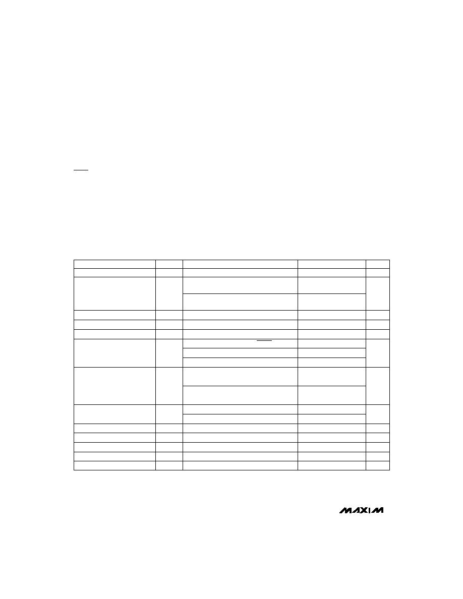
ABSOLUTE MAXIMUM RATINGS
ELECTRICAL CHARACTERISTICS
(+5V
V
IN
+10V, GND = 0V, V
OUT
= -4.1V, R
L
=
, T
A
= T
MIN
to T
MAX
, unless otherwise noted. A 100kHz, 50% duty cycle square
wave between GND and V
IN
is applied to OSC on the MAX852.)
Stresses beyond those listed under "Absolute Maximum Ratings" may cause permanent damage to the device. These are stress ratings only, and functional
operation of the device at these or any other conditions beyond those indicated in the operational sections of the specifications is not implied. Exposure to
absolute maximum rating conditions for extended periods may affect device reliability.
Note 1:
The output may be shorted to NEGOUT or GND if the package power dissipation is not exceeded. Typical short-circuit
current to GND is 50mA.
Note 2:
The supply voltage can drop to 4.5V, but the output may no longer sink 5mA at -4.1V.
Note 3:
The MAX852 will operate with a 50kHz to 250kHz square wave of 40% to 60% duty cycle. For best performance, use an
80kHz to 120kHz square wave with 50% duty cycle.
Supply Voltage, V
IN
to GND ..................................-0.3V to 10.5V
V
NEGOUT
to GND ...................................................-10.5V to 0.3V
V
IN to
V
NEGOUT
.........................................................-0.3V to 21V
V
OUT
to GND (Note 1) ........................................V
NEGOUT
to 0.3V
SHDN or OSC (pin 4) Voltage to GND.........-0.3V to (V
IN
+ 0.3V)
Continuous Power Dissipation (T
A
= +70∞C)
SO (derate 5.88mW/∞C above +70∞C) ........................471mW
Operating Temperature Ranges
MAX85_ISA ......................................................-25∞C to +85∞C
MAX85_ESA.....................................................-40∞C to +85∞C
Storage Temperature Range .............................-65∞C to +160∞C
Lead Temperature (soldering, 10sec) .............................+300∞C
Pin 4
Pin 4
Pin 4
MAX850≠MAX852, V
FB
= 0V,
R
L
=
or 820
, Figure 2a
Pin 4
MAX850/MAX851/MAX853, T
A
= +25∞C
MAX853
MAX850≠MAX852
MAX853, V
CTRL
= 4.1V,
R
L
=
or 820
, Figure 2c
MAX850/MAX853, V
IN
= 10V, SHDN = 0V
MAX850≠MAX852, V
FB
= 0V,
R
L
=
or 820
, Figure 2a
MAX850≠MAX852, no load, Figure 2b
MAX853, V
CTRL
= 4.1V,
R
L
=
or 820
, Figure 2c
MAX852, OSC low
MAX851, SHDN = 2V
CONDITIONS
pF
10
C
IN
Input Capacitance
µA
±1
I
IN
Input Current
V
0.5
V
IL
Input Low Voltage
V
2.0
V
IH
Input High Voltage
kHz
80
100
120
f
OSC
Oscillator Frequency (Note 3)
mVp-p
1
V
OUT
Ripple
2
mV/mA
3
8
V
OUT
Load Regulation
4
8
µA
1
I
SHUT
Shutdown Supply Current
2
5
-4.3
-4.1 -3.9
V
5
10
V
IN
Supply Voltage Range (Note 2)
0.002
1
mA
2.0
3.0
I
Q
Supply Current
V
-1.32
-1.28
-1.24
V
FBset
Set Voltage
V
-0.5 to -(V
IN
- 1)
Output Voltage Range
V
-4.2
-4.0
V
OUT
Output Voltage
UNITS
MIN
TYP
MAX
SYMBOL
PARAMETER
MAX850≠MAX853
Low-Noise, Regulated, Negative
Charge-Pump Power Supplies for GaAsFET Bias
_______________________________________________________________________________________
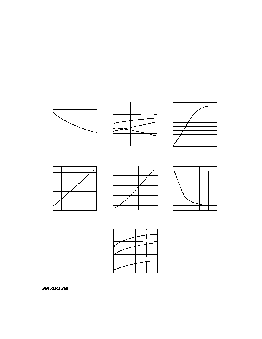
3
-4.10
0
OUTPUT VOLTAGE
vs. OUTPUT CURRENT
MAX850-TOC1
OUTPUT CURRENT (mA)
OUTPUT VOLTAGE (V)
-4.11
-4.14
-4.13
-4.12
-4.15
-4.16
2.0
4.0
6.0
8.0
10.0
-4.06
5.0
OUTPUT VOLTAGE vs.
INPUT VOLTAGE OVER TEMPERATURE
MAX850-TOC2
INPUT VOLTAGE (V)
OUTPUT VOLTAGE (V)
-4.07
-4.11
-4.10
-4.09
-4.08
-4.12
-4.13
-4.12
6.0
7.0
8.0
9.0
10.0
T
A
= +25∞C
T
A
= -40∞C
T
A
= +85∞C
I
OUT
= 2.5mA
10
20
30
40
50
60
5.0
6.0
7.0
8.0
9.0
10.0
MAXIMUM OUTPUT CURRENT
vs. INPUT VOLTAGE
MAX850-TOC3
INPUT VOLTAGE (V)
MAXIMUM OUTPUT CURRENT (mA)
0.60
0.80
1.00
1.20
5.0
6.0
NO-LOAD SUPPLY CURRENT
vs. INPUT VOLTAGE
MAX850-TOC4
INPUT VOLTAGE (V)
NO-LOAD SUPPLY CURRENT (mA)
1.40
1.60
1.80
2.00
9.0
7.0
8.0
10.0
2.5
1.6
-40
-20
20
40
100
SUPPLY CURRENT
vs. TEMPERATURE
1.7
2.2
2.3
2.4
MAX850-TOC5
TEMPERATURE (∞C)
SUPPLY CURRENT (mA)
0
60
80
2.1
2.0
1.9
1.8
V
IN
= 10.0V
0.20
0.40
0.60
0.80
5.0
6.0
START-UP TIME vs.
INPUT VOLTAGE
MAX850-TOC6
INPUT VOLTAGE (V)
START-UP TIME (ms)
1.00
1.20
1.40
1.60
1.80
2.00
9.0
7.0
8.0
10.0
I
OUT
= 5mA
10
20
30
50
60
40
70
80
1.0 1.5
2.0
2.5
3.0
3.5
4.0
4.5 5.0
EFFICIENCY vs. LOAD CURRENT
MAX850-TOC7
LOAD CURRENT (mA)
EFFICIENCY (%)
V
IN
= 6.0V
V
IN
= 5.0V
V
IN
= 10.0V
__________________________________________Typical Operating Characteristics
(Circuit of Figure 2a, V
IN
= 6V, T
A
= +25∞C, unless otherwise noted.)

MAX850≠MAX853
Low-Noise, Regulated, Negative
Charge-Pump Power Supplies for GaAsFET Bias
4
______________________________________________________________________________________
V
IN
= 6.0V, V
OUT
= -4.1V, I
OUT
= 5mA, AC COUPLED
MAX850≠MAX852
OUTPUT NOISE AND RIPPLE
V
OUT
500
µ
V/div
10
µ
s/div
_____________________________Typical Operating Characteristics (continued)
(Circuit of Figure 2a, V
IN
= 6V, T
A
= +25∞C, unless otherwise noted.)
V
IN
= 6.0V, V
OUT
= -4.1V, I
OUT
= 5mA, AC COUPLED
MAX853
OUTPUT NOISE AND RIPPLE
V
OUT
500
µ
V/div
10
µ
s/div
MAX850≠MAX852
NOISE SPECTRUM
70
60
50
40
30
20
10
0
-10
-20
-30
NOISE (dB
µ
V)
0.1
1000
100
10
1.0
FREQUENCY (kHz)
MAX853
NOISE SPECTRUM
70
60
50
40
30
20
10
0
-10
-20
-30
NOISE (dB
µ
V)
0.1
1000
100
10
1.0
FREQUENCY (kHz)
NOTE: dBµV = 20 log V
OUT
1µV

MAX850≠MAX853
Low-Noise, Regulated, Negative
Charge-Pump Power Supplies for GaAsFET Bias
_______________________________________________________________________________________
5
_____________________________Typical Operating Characteristics (continued)
(Circuit of Figure 2a, V
IN
= 6V, T
A
= +25∞C, unless otherwise noted.)
CIRCUIT OF FIGURE 2a, V
IN
= 6.0V, V
OUT
= -4.1V, I
OUT
= 5mA
MAX850/MAX851/MAX853
START-UP FROM SHUTDOWN
V
OUT
2V/div
V
SHDN
5V/div
200
µ
s/div
CIRCUIT OF FIGURE 2a, V
IN
= 6.0V, V
OUT
= -4.1V, I
OUT
= 5mA
SHUTDOWN OCCURS WHEN 100kHz EXTERNAL CLOCK IS GATED OFF
MAX852
START-UP FROM SHUTDOWN
V
OUT
2V/div
V
OSC
5V/div
200
µ
s/div
V
OUT
= -4.08V, I
OUT
= 5mA, AC COUPLED
LINE-TRANSIENT RESPONSE
V
OUT
20mV/div
V
IN
6.0V
5.5V
2ms/div
V
OUT
= -4.0V, AC COUPLED
LOAD-TRANSIENT RESPONSE
I
OUT
0.01mA
5mA
V
OUT
50mV/div
1ms/div