
General Description
The MAX8510/MAX8511/MAX8512 ultra-low-noise, low-
dropout (LDO) linear regulators are designed to deliver up
to 120mA continuous output current from a tiny 5-pin
SC70 plastic package. These regulators achieve a low
120mV dropout for 120mA load current. The MAX8510
uses an advanced architecture to achieve ultra-low output
voltage noise of 11µV
RMS
and PSRR of 54dB at 100kHz.
The MAX8511 does not require a bypass capacitor,
hence achieving the smallest PC board area. The
MAX8512's output voltage can be adjusted with an
external divider.
The MAX8510/MAX8511 are preset to a variety of volt-
ages in the 1.5V to 4.5V range. Designed with a P-
channel MOSFET series pass transistor, the MAX8510/
MAX8511/MAX8512 maintain very low ground current
(40µA).
The regulators are designed and optimized to work with
low-value, low-cost ceramic capacitors. The MAX8510
requires only 1µF (typ) of output capacitance for stability
with any load. When disabled, current consumption drops
to below 1µA.
Applications
Cellular and Cordless Phones
PDA and Palmtop Computers
Base Stations
Bluetooth Portable Radios and Accessories
Wireless LANs
Digital Cameras
Personal Stereos
Portable and Battery-Powered Equipment
Features
Space-Saving 5-Pin SC70 Package
11µV
RMS
Output Noise at 100Hz to 100kHz
Bandwidth (MAX8510)
78dB PSRR at 1kHz (MAX8510)
120mV Dropout at 120mA Load
Stable with 1µF Ceramic Capacitor for Any Load
Guaranteed 120mA Output
Only Need Input and Output Capacitors (MAX8511)
Output Voltages: 1.5V, 1.8V, 2.5V, 2.6V, 2.7V, 2.8V,
2.85V, 3V, 3.3V, 4.5V (MAX8510/MAX8511) and
Adjustable (MAX8512)
Low 40µA Ground Current
Excellent Load/Line Transient
Overcurrent and Thermal Protection
MAX8510/MAX8511/MAX8512
Ultra-Low-Noise, High PSRR,
Low-Dropout,120mA Linear Regulators in SC70
________________________________________________________________ Maxim Integrated Products
1
GND
BP (MAX8510)
N.C. (MAX8511)
FB (MAX8512)
SHDN
1
5
OUT
IN
MAX8510
MAX8511
MAX8512
SC70-5
TOP VIEW
2
3
4
Pin Configuration
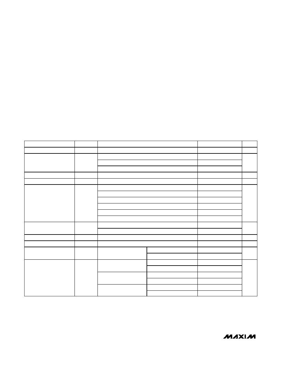
Ordering Information
MAX8510
OUTPUT PRESET
1.5V TO 4.5V
IN
INPUT
2V TO 6V
OFF
SHDN
C
BP
= 10nF
C
OUT
= 1µF
C
IN
= 1µF
OUT
ON
BP
GND
Typical Operating Circuits
19-2732; Rev 1; 6/04
For pricing, delivery, and ordering information, please contact Maxim/Dallas Direct! at
1-888-629-4642, or visit Maxim's website at www.maxim-ic.com.
*xy is the output voltage code (see Output Voltage Selector
Guide). Other versions between 1.5V and 4.5V are available in
100mV increments. Contact factory for other versions.
PART*
TEMP RANGE
PIN-PACKAGE
MAX8510
EXKxy-T
-40∞C to +85∞C
5 SC70-5
MAX8511
EXKxy-T
-40∞C to +85∞C
5 SC70-5
MAX8512
EXK-T
-40∞C to +85∞C
5 SC70-5
Typical Operating Circuits continued at end of data sheet.
Output Voltage Selector Guide appears at end of data sheet.
MAX8510/MAX8511/MAX8512
Ultra-Low-Noise, High PSRR, Low-Dropout,
120mA Linear Regulators in SC70
2
_______________________________________________________________________________________
ABSOLUTE MAXIMUM RATINGS
ELECTRICAL CHARACTERISTICS
(V
IN
= V
OUT
+ 0.5V, T
A
= -40∞C to +85∞C, unless otherwise noted. C
IN
= 1µF, C
OUT
= 1µF, C
BP
= 10nF. Typical values are at +25∞C;
the MAX8512 is tested with 2.45V output, unless otherwise noted.) (Note 1)
Stresses beyond those listed under "Absolute Maximum Ratings" may cause permanent damage to the device. These are stress ratings only, and functional
operation of the device at these or any other conditions beyond those indicated in the operational sections of the specifications is not implied. Exposure to
absolute maximum rating conditions for extended periods may affect device reliability.
IN to GND .................................................................-0.3V to +7V
Output Short-Circuit Duration ............................................Infinite
OUT,
SHDN to GND ......................................-0.3V to (IN + 0.3V)
FB, BP, N.C. to GND..................................-0.3V to (OUT + 0.3V)
Continuous Power Dissipation (T
A
= +70∞C)
5-Pin SC70 (derate 3.1mW/∞C above +70∞C) ..............0.247W
JA
(5-Pin SC70) ...............................................................324∞C/W
Operating Temperature Range ...........................-40∞C to +85∞C
Junction Temperature ......................................................+150∞C
Storage Temperature Range .............................-65∞C to +150∞C
Lead Temperature (soldering, 10s) .................................+300∞C
PARAMETER
SYMBOL
CONDITIONS
MIN
TYP
MAX
UNITS
Input Voltage Range
V
IN
2
6
V
I
OUT
= 1mA, T
A
= +25∞C
-1
+1
I
OUT
= 100µA to 80mA, T
A
= +25∞C
-2
+2
Output Voltage Accuracy
I
OUT
= 100µA to 80mA
-3
+3
%
Maximum Output Current
I
OUT
120
mA
Current Limit
I
LIM
OUT = 90% of nominal value
130
200
300
mA
V
OUT
3V, I
OUT
= 80mA
80
170
V
OUT
3V, I
OUT
= 120mA
120
2.5V
V
OUT
< 3V, I
OUT
= 80mA
90
200
2.5V
V
OUT
< 3V, I
OUT
= 120mA
135
2V
V
OUT
< 2.5V, I
OUT
= 80mA
120
250
Dropout Voltage (Note 2)
2V
V
OUT
< 2.5V, I
OUT
= 120mA
180
mV
I
OUT
= 0.05mA
40
90
Ground Current
I
Q
V
IN
= V
OUT
(nom) - 0.1V, I
OUT
= 0mA
220
500
µA
Line Regulation
V
LNR
V
IN
= (V
OUT
+ 0.5V) to 6V, I
OUT
= 0.1mA
0.001
%/V
Load Regulation
V
LDR
I
OUT
= 1mA to 80mA
0.003
%/mA
T
A
= +25∞C
0.003
1
Shutdown Supply Current
I
SHDN
SHDN = 0V
T
A
= +85∞C
0.05
µA
MAX8510
78
f = 1kHz, I
OUT
= 10mA
MAX8511/MAX8512
72
MAX8510
75
f = 10kHz, I
OUT
= 10mA
MAX8511/MAX8512
65
MAX8510
54
Ripple Rejection
PSRR
f = 100kHz, I
OUT
= 10mA
MAX8511/ MAX8512
46
dB

MAX8510/MAX8511/MAX8512
Ultra-Low-Noise, High PSRR, Low-Dropout,
120mA Linear Regulators in SC70
_______________________________________________________________________________________
3
ELECTRICAL CHARACTERISTICS (continued)
(V
IN
= V
OUT
+ 0.5V, T
A
= -40∞C to +85∞C, unless otherwise noted. C
IN
= 1µF, C
OUT
= 1µF, C
BP
= 10nF. Typical values are at +25∞C;
the MAX8512 is tested with 2.45V output, unless otherwise noted.) (Note 1)
Note 1:
Limits are 100% tested at +25∞C. Limits over operating temperature range are guaranteed by design.
Note 2:
Dropout is defined as V
IN
- V
OUT
when V
OUT
is 100mV below the value of V
OUT
for V
IN
= V
OUT
+ 0.5V.
Note 3:
Time needed for V
OUT
to reach 90% of final value.
PARAMETER
SYMBOL
CONDITIONS
MIN
TYP
MAX
UNITS
MAX8510
11
f = 100Hz to 100kHz,
I
LOAD
= 10mA
MAX8511/MAX8512
230
MAX8510
13
Output Noise Voltage
(RMS)
f = 100Hz to 100kHz,
I
LOAD
= 80mA
MAX8511/MAX8512
230
µV
Shutdown Exit Delay
R
LOAD
= 50
(Note3)
300
µs
SHDN Logic Low Level
V
IN
= 2V to 6V
0.4
V
SHDN Logic High Level
V
IN
= 2V to 6V
1.5
V
T
A
= +25∞C
SHDN Input Bias Current
V
IN
= 6V, SHDN = 0V or
6V
T
A
= +85∞C
0.01
µA
T
A
= +25∞C
0.006
0.1
FB Input Bias Current
(MAX8512)
V
IN
= 6V,V
FB
= 1.3V
T
A
= +85∞C
0.01
µA
Thermal Shutdown
160
∞C
Thermal-Shutdown
Hysteresis
10
∞C
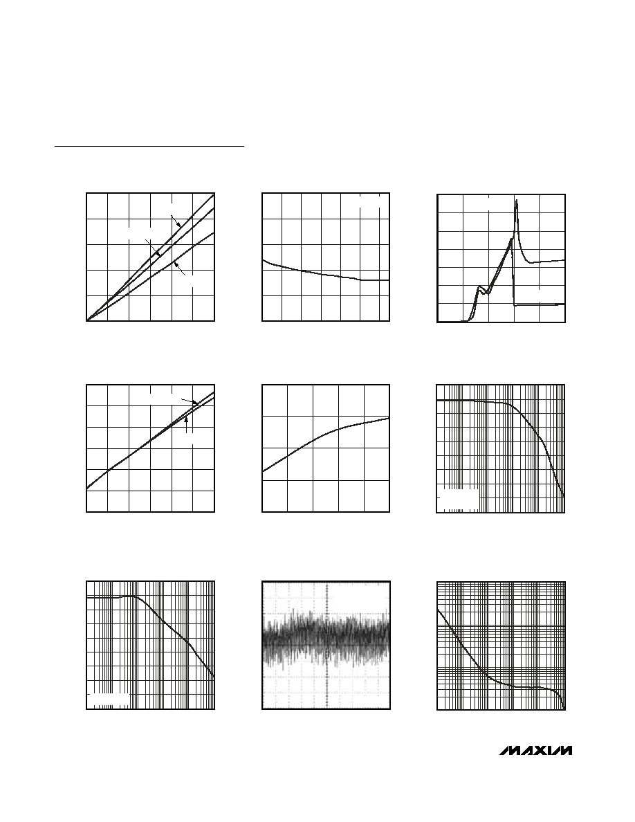
Typical Operating Characteristics
(V
IN
= V
OUT
+ 0.5V, C
IN
= 1µF, C
OUT
= 1µF, C
BP
= 10nF, T
A
= +25∞C, unless otherwise noted.)
MAX8510
OUTPUT VOLTAGE vs. INPUT VOLTAGE
MAX8510 toc01
INPUT VOLTAGE (V)
OUTPUT VOLTAGE (V)
5
4
3
2
1
0.5
1.0
1.5
2.0
2.5
3.0
0.0
0
6
I
OUT
= 120mA
I
OUT
= 0mA
MAX8510
OUTPUT VOLTAGE ACCURACY
vs. LOAD CURRENT
MAX8510 toc02
LOAD CURRENT (mA)
% DEVIATION (%)
100
80
60
40
20
-0.4
-0.2
0
0.2
0.4
0.6
-0.6
0
120
MAX8510
OUTPUT VOLTAGE ACCURACY
vs. TEMPERATURE
MAX8510 toc03
TEMPERATURE (∞C)
% DEVIATION (%)
60
35
10
-15
-0.8
-0.6
-0.4
-0.2
0
0.2
0.4
0.6
0.8
1.0
-1.0
-40
85
IOUT = 1mA
MAX8510/MAX8511/MAX8512
Ultra-Low-Noise, High PSRR, Low-Dropout,
120mA Linear Regulators in SC70
4
_______________________________________________________________________________________
Typical Operating Characteristics (continued)
(V
IN
= V
OUT
+ 0.5V, C
IN
= 1µF, C
OUT
= 1µF, C
BP
= 10nF, T
A
= +25∞C, unless otherwise noted.)
MAX8510
DROPOUT VOLTAGE vs. LOAD CURRENT
MAX8510 toc04
LOAD CURRENT (mA)
DROPOUT VOLTAGE (mV)
100
80
60
40
20
30
60
90
120
150
0
0
120
T
A
= +85∞C
T
A
= +25∞C
T
A
= -40∞C
MAX8510
DROPOUT VOLTAGE vs. OUTPUT VOLTAGE
MAX8510 toc05
OUTPUT (V)
DROPOUT VOLTAGE (mV)
3.0
2.8
2.6
2.4
2.2
50
100
150
200
250
0
2.0
3.2
I
OUT
= 80mA
MAX8510
GROUND PIN CURRENT vs. INPUT VOLTAGE
MAX8510 toc06
INPUT VOLTAGE (V)
GROUND PIN CURRENT (
µ
A)
4
3
2
1
150
200
50
100
250
300
350
0
0
5
I
OUT
= 120mA
I
OUT
= 0mA
MAX8510
GROUND PIN CURRENT vs. LOAD CURRENT
MAX8510 toc 07
LOAD CURRENT (mA)
GROUND PIN CURRENT (
µ
A)
100
80
60
40
20
40
80
120
160
200
240
0
0
120
V
IN
= 3.8V
V
IN
= 5.5V
MAX8510
GROUND PIN CURRENT vs. TEMPERATURE
MAX8510 toc08
TEMPERATURE (∞C)
GROUND PIN CURRENT (
µ
A)
60
35
10
-15
35
40
45
50
30
-40
85
MAX8510
PSRR vs. FREQUENCY
MAX8510 toc09
FREQUENCY (kHz)
PSRR (dB)
1
10
100
0.1
40
50
60
10
20
30
70
80
90
0
0.01
1000
I
LOAD
= 10mA
C
BP
= 10nF
MAX8511
PSRR vs. FREQUENCY
MAX8510 toc10
FREQUENCY (kHz)
PSRR (dB)
0.1
1
10
100
40
50
60
10
20
30
70
80
90
0
0.01
1000
I
LOAD
= 10mA
MAX8510
OUTPUT NOISE
MAX8510 toc11
400µs/div
V
IN
= 3.8V
I
LOAD
= 10mA
V
NOISE
= 11µV
RMS
20µV/div
MAX8510
OUTPUT NOISE SPECTRAL DENSITY
vs. FREQUENCY
MAX8510 toc12
FREQUENCY (kHz)
OUTPUT NOISE DENSITY (nV/
Hz
)
0.1
1
10
100
1.E+03
1.E+02
1.E+04
1.E+01
0.01
1000

MAX8510/MAX8511/MAX8512
Ultra-Low-Noise, High PSRR, Low-Dropout,
120mA Linear Regulators in SC70
_______________________________________________________________________________________
5
Typical Operating Characteristics (continued)
(V
IN
= V
OUT
+ 0.5V, C
IN
= 1µF, C
OUT
= 1µF, C
BP
= 10nF, T
A
= +25∞C, unless otherwise noted.)
MAX8510
OUTPUT NOISE vs. BP CAPACITANCE
MAX8510 toc13
BP CAPACITANCE (nF)
OUTPUT NOISE (
µ
V)
10
5
10
15
20
25
0
1
100
MAX8510
LOAD TRANSIENT RESPONSE
MAX8510 toc14
1ms/div
V
IN
= 3.5V
I
LOAD
= 0 TO 50mA
V
OUT
10mV/div
MAX8510
LOAD TRANSIENT RESPONSE NEAR DROPOUT
MAX8510 toc15
1ms/div
V
IN
= 3.1V
I
LOAD
= 0 TO 50mA
V
OUT
10mV/div
MAX8510
LINE TRANSIENT RESPONSE
MAX8510 toc16
200µs/div
V
IN
= 3.5V TO 4V
V
OUT
2mV/div
MAX8510
EXITING SHUTDOWN WAVEFORM
MAX8510 toc17
20µs/div
V
OUT
= 2.85V
R
LOAD
= 47
OUTPUT VOLTAGE
2V/div
SHUTDOWN VOLTAGE
MAX8510
ENTERING SHUTDOWN DELAY
MAX8510 toc18
40µs/div
C
BP
= 0.01µF
OUTPUT VOLTAGE
2V/div
SHUTDOWN
VOLTAGE
MAX8510
SHUTDOWN EXIT DELAY
MAX8510 toc19
20µs/div
V
OUT
1V/div
SHUTDOWN
VOLTAGE
V
OUT
= 3V
C
BP
= 100nF
MAX8510
REGION OF STABLE C
OUT
ESR
vs. LOAD CURRENT
MAX8510 toc20
LOAD CURRENT (mA)
C
OUT
ESR (
)
80
60
40
20
0.1
1
10
100
0.01
0
120
100
STABLE REGION