General Description
The MAX8530/MAX8531 offer the benefits of low-
dropout voltage and ultra-low power regulation in
subminiaturized UCSP and QFN packages with an inte-
grated microprocessor reset circuit (MAX8530 only).
The devices operate from a 2.5V to 6.5V input and
deliver up to 200mA and 150mA outputs with low
dropout of 100mV (typ) at 100mA. Designed with an
internal P-channel MOSFET pass transistor, the supply
current is kept at a low 130µA (with both LDOs on),
independent of the load current and dropout voltage.
Other features include short-circuit protection and
thermal-shutdown protection.
The MAX8530 provides microprocessor open-drain,
active-low reset output to monitor OUT1, eliminating
external components and adjustments. The MAX8530
asserts a 100ms (min) RESET signal when OUT1 drops
below 87% of the nominal output voltage. The MAX8531
includes a reference bypass pin for low output noise
(40µV
RMS
).
Both devices include a logic-controlled shutdown input
and are available in 6-bump UCSP and 6-pin thin QFN
exposed pad packages.
Applications
Cellular and Cordless Phones
PDAs and Palmtop Computers
Notebook Computers
Digital Cameras
PCMCIA Cards
Wireless LAN Cards
Hand-Held Instruments
Features
o Guaranteed 200mA Output Current for OUT1
o Guaranteed 150mA Output Current for OUT2
o Low 100mV (typ) Dropout at 100mA Load for
both LDOs
o Open-Drain, Active-Low 100ms (min) Reset Timer
(MAX8530)
o Low 40µV
RMS
Output Noise (MAX8531)
o Low 130µA Operating Supply Current
o <1µA Shutdown Current
o Thermal-Overload and Short-Circuit Protection
o Output Current Limit
o Tiny Packages Available
1.16 x 1.57 x 0.6mm UCSP (3 x 2 Grid)
3mm x 3mm Thin QFN
MAX8530/MAX8531
Dual Low-Dropout Linear Regulators
with
RESET
or Low-Noise Output in UCSP or QFN
Ordering Information
19-2711; Rev 0; 1/03
For pricing, delivery, and ordering information, please contact Maxim/Dallas Direct! at
1-888-629-4642, or visit Maxim's website at www.maxim-ic.com.
*xy = Output voltage code (see the Output Voltage Selector
Guide).
**EP = Exposed pad.
EVALUATION KIT
AVAILABLE
Pin Configurations appear at end of data sheet.
Output Voltage Selector Guide appears at end of data
sheet.
PART
TEMP RANGE
OUT_
VOLTAGE
PIN-
PACKAGE
M A X8 5 3 0 E BTxy* - 40
∞ C to + 85∞ C 1.5V to 3.3V 6 U C S P
M AX 8530E TTxy* - 40
∞ C to + 85∞ C 1.5V to 3.3V 6 Thi n Q FN - E P **
M A X8 5 3 1 E BTxy* - 40
∞ C to + 85∞ C 1.5V to 3.3V 6 U C S P
M AX 8531E TTxy* - 40
∞ C to + 85∞ C 1.5V to 3.3V 6 Thi n Q FN - E P
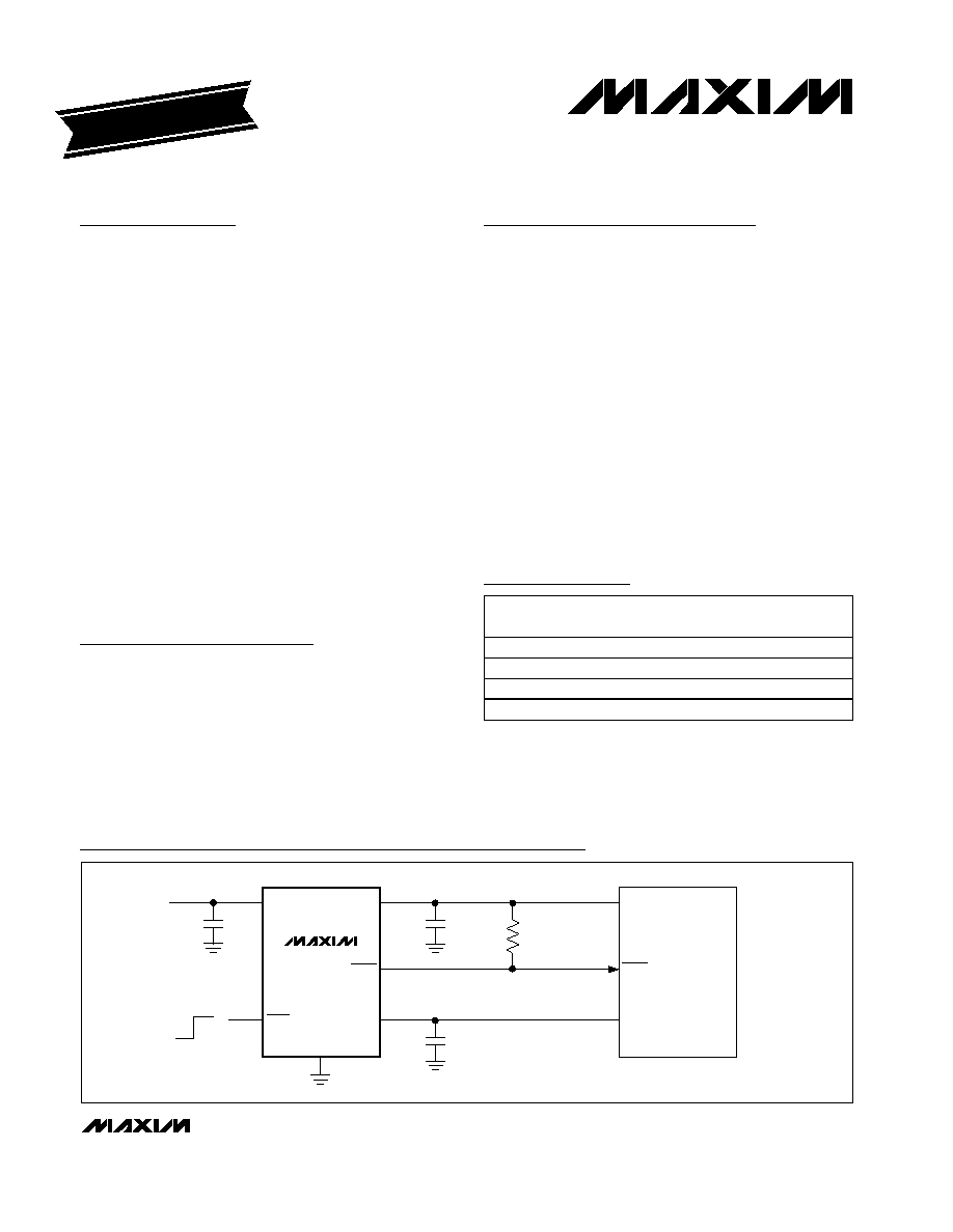
IN
OUT1
2.2
µF
C
IN
2.2
µF
INPUT
2.5V TO 6.5V
1.5V TO 3.3V
AT 200mA
1.5V TO 3.3V
AT 150mA
1
µF
SHDN
OFF
ON
OUT2
GND
RESET
BASEBAND
µP
V
I/O
V
CORE
RESET
MAX8530
Typical Operating Circuit

MAX8530/MAX8531
Dual Low-Dropout Linear Regulators
with
RESET
or Low-Noise Output in UCSP or QFN
2
_______________________________________________________________________________________
ABSOLUTE MAXIMUM RATINGS
ELECTRICAL CHARACTERISTICS
(IN = 3.8V, SHDN = IN, C
BP
= 10nF (MAX8531), T
A
= -40∞C to +85∞C, unless otherwise noted. Typical values are at T
A
= +25∞C.)
(Note 2)
Stresses beyond those listed under "Absolute Maximum Ratings" may cause permanent damage to the device. These are stress ratings only, and functional
operation of the device at these or any other conditions beyond those indicated in the operational sections of the specifications is not implied. Exposure to
absolute maximum rating conditions for extended periods may affect device reliability.
IN, SHDN, RESET, BP to GND .................................-0.3V to +7V
OUT1, OUT2 to GND...................................-0.3V to (VIN + 0.3V)
Output Short-Circuit Duration ........................................Indefinite
Continuous Power Dissipation (TA = +70∞C)
6-Bump UCSP (derate 3.9mW/
∞C above +70∞C) ........308mW
6-Lead QFN (derate 24.4mW/
∞C above +70∞C) ........1951mW
Operating Temperature Range ...........................-40
∞C to +85∞C
Junction Temperature ......................................................+150
∞C
Storage Temperature Range .............................-65
∞C to +150∞C
6-Bump+ UCSP Solder Profile ....................................(Note 1)
6-Lead QFN Lead Temperature (10s) .........................+300
∞C
PARAMETER
SYMBOL
CONDITIONS
MIN
TYP
MAX
UNITS
Input Voltage
V
IN
2.5
6.5
V
Undervoltage Lockout Threshold
V
UVLO
IN rising, hysteresis is 40mV (typ)
2.15
2.25
2.42
V
T
A
= +25∞C, I
OUT1
= I
OUT2
= 1mA
-1
+1
T
A
= -40∞C to +85∞C, I
OUT1
= I
OUT2
= 1mA
-2
+2
Output Voltage Accuracy
T
A
= - 40∞C to + 85∞ C , I
OU T 1
= 0.1m A to 200m A,
I
OU T 2
= 0.1m A to 150m A
-3
+3
%
OUT1
200
Maximum Output Current
I
OUT_
OUT2
150
mA
OUT1
210
330
550
Current Limit
I
LIM
OUT2
165
280
500
mA
No load
130
220
Ground Current
I
Q
I
OUT1
= I
OUT2
= 100mA
150
µA
Dropout Voltage
V
OUT_
- V
IN
I
OUT_
= 100mA (Note 3)
100
200
mV
Line Regulation
V
LNR
IN = (OUT_ + 0.1V) to 3.8V
-0.2
+0.2
%/V
MAX8530
320
Output Voltage Noise
10Hz to 100kHz, C
OUT
= 10µF,
I
OUT
= 10mA
MAX8531
40
µV
RMS
MAX8530
60
Ripple Rejection
PSRR
100Hz, I
OUT
= 30mA
MAX8531
62
dB
SHUTDOWN
SHDN = 0, T
A
= +25∞C
0.01
1
SHDN Supply Current
I
OFF
SHDN = 0, T
A
= +85∞C
0.1
µA
V
IH
Input high voltage
1.6
SHDN Input Threshold
V
IL
Input low voltage
0.4
V
T
A
= +25∞C
0.7
100
SHDN Input Bias Current
I
SHDN
SHDN = IN or GND
T
A
= +85∞C
0.8
nA
THERMAL PROTECTION
Thermal-Shutdown Temperature
T
SHDN
T
J
rising
160
∞C
Thermal-Shutdown Hysteresis
T
SHDN
10
∞C
Note 1: For UCSP solder profile information, visit www.maxim-ic.com/1st_pages/UCSP.html.
MAX8530/MAX8531
Dual Low-Dropout Linear Regulators
with
RESET
or Low-Noise Output in UCSP or QFN
_______________________________________________________________________________________
3
ELECTRICAL CHARACTERISTICS (continued)
(IN = 3.8V, SHDN = IN, C
BP
= 10nF (MAX8531), T
A
= -40∞C to +85∞C, unless otherwise noted. Typical values are at T
A
= +25∞C.)
(Note 2)
Note 2: All units are 100% production tested at T
A
= +25∞C. Limits over the operating temperature range are guaranteed by design.
Note 3: The dropout voltage is defined as V
IN
- V
OUT
, when V
OUT
is 100mV below the value of V
OUT
for V
IN
= V
OUT
+ 0.5V.
Specification applies only when V
OUT
2.5V.
PARAMETER
SYMBOL
CONDITIONS
MIN
TYP
MAX
UNITS
RESET OUTPUT (MAX8530 ONLY)
RESET Threshold
V
TH
Percentage of nominal output, OUT1 falling,
when RESET falls.
84
87
89
%
RESET Threshold Hysteresis
0.5
%
I
RESET
= 500µA, IN = 3.8V
10
20
RESET Output Voltage Low
(Open-Drain, Active Low)
V
OL
I
RESET
= 100µA, IN = 1.2V
10
40
mV
T
A
= +25∞C
0.001
1
RESET Open-Drain
Output Leakage Current
V
RESET
= 6.5V
T
A
= +85∞C
0.01
µA
RESET Active Timeout Delay
From OUT1 rising to RESET rising.
100
200
360
ms
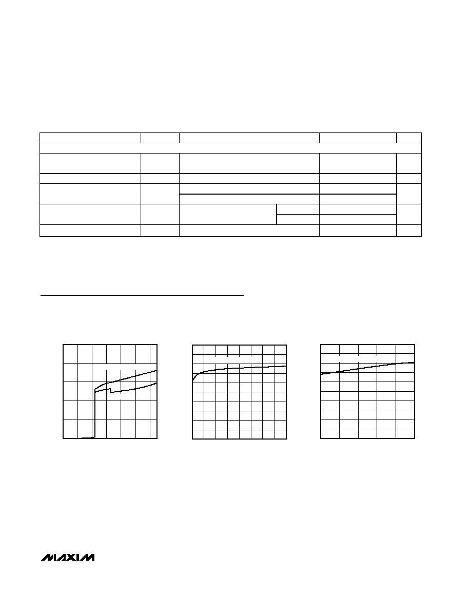
Typical Operating Characteristics
V
OUT1
= 3.3V, V
OUT2
= 1.5V, load = 80mA (both output voltages), V
IN
= 3.8V, C
OUT_
= 2.2µF, C
BP
= 0.01µF, C
IN
= 2.2µF, and T
A
= +25∞C,
unless otherwise noted.
SUPPLY CURRENT
vs. SUPPLY VOLTAGE
MAX8530 toc01
SUPPLY VOLTAGE (V)
SUPPLY CURRENT (
µ
A)
6
5
4
3
2
1
50
100
150
200
250
0
0
80mA LOAD, BOTH OUTPUTS
NO LOAD
SUPPLY CURRENT
vs. LOAD CURRENT
MAX8530 toc02
LOAD CURRENT (mA)
SUPPLY CURRENT (
µ
A)
70
60
40
50
20
30
10
20
40
60
80
100
120
140
160
180
200
0
0
80
BOTH OUTPUTS LOADED
SUPPLY CURRENT
vs. TEMPERATURE
MAX8530 toc03
TEMPERATURE (
∞C)
SUPPLY CURRENT (
µ
A)
60
35
10
-15
20
40
60
80
100
120
140
160
180
200
0
-40
85
80mA LOAD, BOTH OUTPUTS

MAX8530/MAX8531
Dual Low-Dropout Linear Regulators
with
RESET
or Low-Noise Output in UCSP or QFN
4
_______________________________________________________________________________________
Typical Operating Characteristics (continued)
V
OUT1
= 3.3V, V
OUT2
= 1.5V, load = 80mA (both output voltages), V
IN
= 3.8V, C
OUT_
= 2.2µF, C
BP
= 0.01µF, C
IN
= 2.2µF, and T
A
= +25∞C,
unless otherwise noted.
DROPOUT VOLTAGE
vs. LOAD CURRENT
MAX8530 toc04
LOAD CURRENT (mA)
DROPOUT VOLTAGE (mV)
180
160
140
120
100
80
60
40
20
50
100
150
200
250
0
0
200
LDO DROPOUT VOLTAGE vs. V
OUT
MAX8530 toc05
V
OUT
(V)
DROPOUT VOLTAGE (mV)
3.2
3.1
3.0
2.9
2.8
2.7
2.6
20
40
60
80
100
120
0
2.5
3.3
I
OUT1
= 80mA
OUTPUT VOLTAGE ACCURACY
vs. TEMPERATURE
MAX8530 toc06
TEMPERATURE (
∞C)
OUTPUT VOLTAGE (%)
60
35
10
-15
-0.8
-0.6
-0.4
-0.2
0
0.2
0.4
0.6
0.8
1.0
-1.0
-40
85
PSRR vs. FREQUENCY
MAX8530 toc07
FREQUENCY (kHz)
PSRR (dB)
100
10
1
0.1
10
20
30
40
50
60
70
0
0.01
1000
OUT2 = 2.85V
OUT1 = 2.85V
100
LOAD
CHANNEL-TO-CHANNEL ISOLATION
vs. FREQUENCY (MAX8531)
MAX8530 toc08
FREQUENCY (kHz)
CHANNEL-TO-CHANNEL ISOLATION (dB)
100
10
0.1
1
10
20
30
40
50
60
70
80
0
0.01
1000
100
LOAD
OUTPUT NOISE SPECTRAL DENSITY
vs. FREQUENCY (MAX8531)
MAX8530 toc09
FREQUENCY (kHz)
NOISE DENSITY (nV
RMS
/
Hz)
10
1
0.1
100
1000
10,000
10
0.01
100
OUTPUT NOISE (10Hz TO 100kHz)
(MAX8531)
MAX8530 toc10
V
OUT_
500
µV/
div
10ms/div
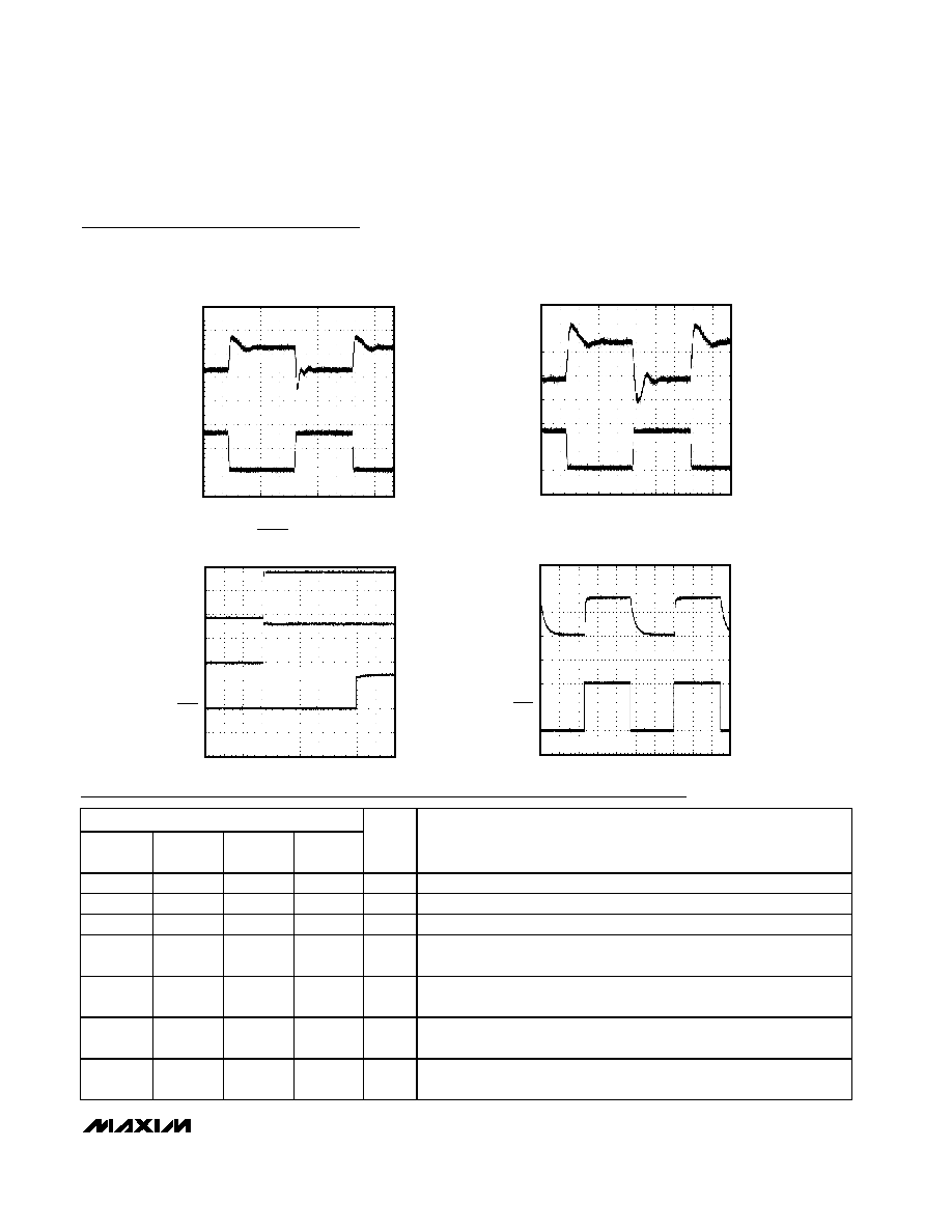
LINE TRANSIENT
MAX8530 toc11
V
OUT_
4.5V
40
µs/div
V
IN
3.5V
1V/div
20mV/div
AC-COUPLED
MAX8530/MAX8531
Dual Low-Dropout Linear Regulators
with
RESET
or Low-Noise Output in UCSP or QFN
_______________________________________________________________________________________
5
LOAD TRANSIENT
(V
IN
= 3.8V, I
LOAD
= 1mA TO 80mA)
MAX8530 toc12
I
LOAD
50mA/div
10
µs/div
V
OUT
0
20mV/div
AC-COUPLED
Pin Description
PIN
MAX8530
(QFN)
MAX8531
(QFN)
MAX8530
(UCSP)
MAX8531
(UCSP)
NAME
FUNCTION
1
1
B3
B3
OUT2
Regulator 2 Output. Guaranteed 150mA output current.
2
2
B2
B2
IN
Regulator Input
3
3
B1
B1
OUT1
Regulator 1 Output. Guaranteed 200mA output current.
4
4
A1
A1
GND
Ground. Also functions as a heatsink for the 6-pin QFN. Solder to a large
pad or the circuit board ground plane to maximize thermal dissipation.
5
5
A2
A2
SHDN
Shutdown Input. A logic low shuts down both regulators. Connect to IN
for normal operation.
6
--
A3
--
RESET
Reset Active-Low Open-Drain Output. Minimum timeout of 100ms. RESET
is low in shutdown.
--
6
--
A3
BP
Reference Noise Bypass. Connect to a 0.01µF ceramic capacitor for
reduced noise at both outputs.
Typical Operating Characteristics (continued)
V
OUT1
= 3.3V, V
OUT2
= 1.5V, load = 80mA (both output voltages), V
IN
= 3.8V, C
OUT_
= 2.2µF, C
BP
= 0.01µF, C
IN
= 2.2µF, and T
A
= +25∞C,
unless otherwise noted.
LOAD TRANSIENT NEAR DROPOUT
MAX8530 toc13
I
LOAD
50mA/div
10
µs/div
V
OUT
0
20mV/div
AC-COUPLED
V
IN
= V
OUT
+ 0.1V
RESET RESPONSE
(MAX8530)
MAX8530 toc14
V
OUT-
2V/
div
40ms/div
V
IN
0
V
RESET
2V/
div
0
2V/
div
0
SHUTDOWN RESPONSE
MAX8530 toc15
V
OUT-
1V/
div
1ms/div
0
V
SHDN
2V/
div
0