
General Description
The MAX8559 dual, low-noise, low-dropout (LDO) linear
regulator operates from a 2.5V to 6.5V input voltage
and delivers at least 300mA of continuous output cur-
rent. It offers low output noise and low dropout of only
60mV at 100mA. Typical output noise for this device is
32µV
RMS
, and PSRR is 70dB at 10kHz. Designed with
an internal P-channel MOSFET pass transistor, the
MAX8559 maintains a low 115µA supply current per
LDO, independent of the load current and dropout volt-
age. Other features include short-circuit protection and
thermal-shutdown protection. The MAX8559 includes
two independent logic-controlled shutdown inputs and
is capable of operating without a bypass capacitor to
further reduce total solution size. The MAX8559 is avail-
able in a miniature 8-bump UCSP (2mm x 1mm) or
8-pin TDFN (3mm x 3mm) package.
Applications
Cellular and Cordless Phones
PDAs and Palmtop Computers
Notebook Computers
Digital Cameras
PCMCIA Cards
Wireless LAN Cards
Hand-Held Instruments
Features
Two Low-Dropout-Voltage Regulators
Low 32µV
RMS
Output Noise
300mA Output Current for Each LDO
70dB PSRR at 10kHz
Independent Shutdown Controls
Low 60mV Dropout at 100mA Load
115µA Operating Supply Current per LDO
1.5V to 3.3V Factory-Preset Output
Small Ceramic Output Capacitors
Output Current Limit
Thermal-Overload and Short-Circuit Protection
1.95W Power-Dissipation Capability (TDFN)
2mm
2
Footprint (UCSP)
MAX8559
Dual, 300mA, Low-Noise Linear Regulator
with Independent Shutdown in UCSP or TDFN
________________________________________________________________ Maxim Integrated Products
1
Ordering Information
ON
OFF
ON
OFF
MAX8559
INPUT
2.5V TO 6.5V
2.2µF
min
INB
SHDNA
SHDNB
INA
GND
OUTB
OUTA
BP
0.01µF
(OPTIONAL)
2.2µF/150mA
4.7µF/300mA
1.5V TO 3.3V
2.2µF/150mA
4.7µF/300mA
1.5V TO 3.3V
Typical Operating Circuit
19-3121; Rev 0; 1/04
For pricing, delivery, and ordering information, please contact Maxim/Dallas Direct! at
1-888-629-4642, or visit Maxim's website at www.maxim-ic.com.
EVALUATION KIT
AVAILABLE
PART
TEMP RANGE
PIN-PACKAGE
MAX8559EBAxy*
-40
∞
C to +85
∞
C
8 UCSP (B8-1)
MAX8559ETAxy*
-40
∞
C to +85
∞
C
8 TDFN-EP**
*
xy = Output voltage code (see the Output Voltage
Selector Guide).
**EP = Exposed pad.
Future product--contact factory for availability.
Output Voltage Selector Guide appears at end of data sheet.
Pin Configurations
GND
OUTB
INB
1
2
OUTA
BP
SHDNA
SHDNB
INA
TDFN
3mm x 3mm
3
4
MAX8559ETA
8
7
6
5
TOP VIEW
Pin Configurations continued at end of data sheet.
MAX8559
Dual, 300mA, Low-Noise Linear Regulator
with Independent Shutdown in UCSP or TDFN
2
_______________________________________________________________________________________
ABSOLUTE MAXIMUM RATINGS
Stresses beyond those listed under "Absolute Maximum Ratings" may cause permanent damage to the device. These are stress ratings only, and functional
operation of the device at these or any other conditions beyond those indicated in the operational sections of the specifications is not implied. Exposure to
absolute maximum rating conditions for extended periods may affect device reliability.
INA, INB,
SHDNA, SHDNB, BP to GND ...................-0.3V to +7V
INA to INB..............................................................-0.3V to +0.3V
OUTA, OUTB to GND ..................................-0.3V to (V
IN
+ 0.3V)
Output Short-Circuit Duration.....................................Continuous
Continuous Power Dissipation (T
A
= +70∞C)
8-Bump UCSP (derate 4.7mW/∞C above +70∞C)..........379mW
8-Pin TDFN (derate 24.4mW/∞C above +70∞C) ..........1951mW
Operating Temperature Range ...........................-40∞C to +85∞C
Junction Temperature ......................................................+150∞C
Storage Temperature Range .............................-65∞C to +150∞C
8-Pin TDFN Lead Temperature (soldering, 10s)..............+300∞C
8-Bump UCSP Solder Profile...........................................(Note 1)
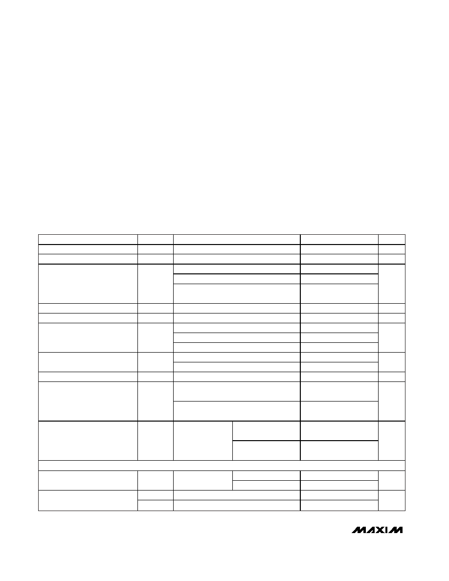
ELECTRICAL CHARACTERISTICS
(V
IN
= 3.8V, SHDNA = SHDNB = IN_, T
A
= -40∞C to +85∞C, unless otherwise noted. Typical values are at T
A
= +25∞C.) (Note 1)
PARAMETER
SYMBOL
CONDITIONS
MIN
TYP
MAX
UNITS
Input Voltage
V
IN
2.5
6.5
V
Undervoltage-Lockout Threshold
V
UVLO
V
IN
rising, hysteresis is 40mV (typ)
2.15
2.35
2.45
V
T
A
= +25
∞
C, I
OUTA
= I
OUTB
= 1mA
-1
+1
T
A
= -40
∞
C to +85
∞
C, I
OUTA
= I
OUTB
= 1mA
-2
+2
Output Voltage Accuracy
T
A
= -40
∞
C to +85
∞
C, I
OUTA
or I
OUTB
=
0.1mA to 300mA
-3
+3
%
Maximum Output Current
I
OUT_
300
mA
Output Current Limit
I
LIM_
310
550
920
mA
No load
180
290
No load, one LDO shutdown
115
Ground Current
I
Q
I
OUTA
= I
OUTB
= 100mA
220
µA
I
OUT_
= 1mA
0.6
Dropout Voltage
(Note 2)
V
OUT_
-
V
IN_
I
OUT_
= 100mA
60
120
mV
Line Regulation
V
LNR
V
IN_
= (V
OUT_
+ 0.1V) to 6.5V, I
OUT_
= 1mA
-0.15
0
+0.15
%/
V
100Hz to 100kHz, C
OUT_
= 10µF,
I
OUT_
= 1mA, C
BP
= 0.01µF
32
Output Voltage Noise
100Hz to 100kHz, C
OUT_
= 10µF,
I
OUT_
= 1mA, C
BP
= not installed
254
µV
RMS
10kHz
70
Power-Supply Ripple Rejection
PSRR
V
IN_
= V
OUT_
+ 1V,
C
BP
= 0.01µF,
C
OUT_
= 2.2µF,
I
OUT_
= 50mA
100kHz
54
dB
SHUTDOWN
T
A
= +25
∞
C
0.01
1
Shutdown Supply Current
I
SHDN
SHDN_ = 0V
T
A
= -40
∞
C to +85
∞
C
0.1
µA
V
IH
Input high voltage
1.6
SHDN Input Threshold
V
IL
Input low voltage
0.4
V
Note 1:
For UCSP solder profile information, please refer to the application note APP_1891 on the Maxim website, www.maxim-ic.com.

MAX8559
Dual, 300mA, Low-Noise Linear Regulator
with Independent Shutdown in UCSP or TDFN
_______________________________________________________________________________________
3
ELECTRICAL CHARACTERISTICS (continued)
(V
IN
= 3.8V, SHDNA = SHDNB = IN_, T
A
= -40∞C to +85∞C, unless otherwise noted. Typical values are at T
A
= +25∞C.) (Note 1)
PARAMETER
SYMBOL
CONDITIONS
MIN
TYP
MAX
UNITS
T
A
= +25∞C
10
100
SHDN Input Bias Current
I
SHDN
SHDN_ = IN or
GND
T
A
= -40
∞
C to +85
∞
C
100
nA
V
OUT_
Discharge Resistance in
Shutdown
SHDN_ = GND
385
THERMAL PROTECTION
Thermal-Shutdown Temperature
T
SHDN
T
J
rising
+160
∞
C
Thermal-Shutdown Hysteresis
T
SHDN
10
∞
C
Note 1:
All units are 100% production tested at T
A
= +25∞C. Limits over the operating temperature range are guaranteed by design.
Note 2:
The dropout voltage is defined as V
IN
- V
OUT
when V
OUT
is 100mV below the nominal value of V
OUT
. Specification only
applies when V
OUT
2.5V.
Typical Operating Characteristics
(V
OUTA
= V
OUTB
= 2.85V, V
INA
= V
INB
= 3.8V, C
OUT
= 2.2µF (or 4.7µF for 300mA), C
BP
= 0.01µF, and C
IN
= 2.2µF (or 4.7µF for
300mA), unless otherwise noted.)
0
100
50
200
150
250
300
0
3
4
1
2
5
6
GROUND CURRENT
vs. SUPPLY VOLTAGE
MAX8559 toc01
SUPPLY VOLTAGE (V)
GROUND CURRENT (
µ
A)
100mA LOAD, BOTH OUTPUTS
NO LOAD, BOTH OUTPUTS
0
50
25
125
100
75
200
175
150
225
0
100
50
150
200
250
300
GROUND CURRENT
vs. LOAD CURRENT
MAX8559 toc02
LOAD CURRENT (mA)
GROUND CURRENT (
µ
A)
BOTH OUTPUTS LOADED
0
75
50
25
100
125
150
175
200
225
250
-40
10
-15
35
60
85
GROUND CURRENT
vs. TEMPERATURE
MAX8559 toc03
TEMPERATURE (∞C)
GROUND CURRENT (
µ
A)
100mA LOAD, BOTH OUTPUTS
NO LOAD, BOTH OUTPUTS

MAX8559
Dual, 300mA, Low-Noise Linear Regulator
with Independent Shutdown in UCSP or TDFN
4
_______________________________________________________________________________________
0
60
40
20
80
100
120
140
160
180
200
0
100
50
150
200
300
DROPOUT VOLTAGE
vs. LOAD CURRENT
MAX8559 toc04
LOAD CURRENT (mA)
DROPOUT VOLTAGE (mV)
250
-0.7
-0.5
-0.6
-0.3
-0.4
-0.1
-0.2
0
0
100
150
50
200
250
300
OUTPUT VOLTAGE ACCURACY
vs. LOAD CURRENT
MAX8559 toc05
LOAD CURRENT (mA)
OUTPUT VOLTAGE ACCURACY (%)
-0.6
-0.3
-0.4
-0.5
-0.2
-0.1
0
0.1
0.2
0.3
0.4
-40
10
-15
35
60
85
OUTPUT VOLTAGE ACCURACY
vs. TEMPERATURE
MAX8559 toc06
TEMPERATURE (∞C)
OUTPUT VOLTAGE ACCURACY (%)
100mA LOAD, BOTH OUTPUTS
100mA LOAD, BOTH OUTPUTS
PSRR vs. FREQUENCY
MAX8559 toc07
FREQUENCY (kHz)
PSRR (dB)
100
10
0.1
1
10
20
30
40
50
60
70
80
0
0.01
1000
I
OUTA
= 50mA
CHANNEL-TO-CHANNEL ISOLATION
vs. FREQUENCY
MAX8559 toc08
FREQUENCY (kHz)
CHANNEL-TO-CHANNEL ISOLATION (dB)
100
10
1
0.1
10
20
30
40
50
60
70
80
90
100
0
0.01
1000
I
OUTA
= 10mA
OUTPUT-NOISE SPECTRAL DENSITY
vs. FREQUENCY
MAX8559 toc09
FREQUENCY (kHz)
NOISE DENSITY (nV/
Hz)
10
1
0.1
100
1000
10,000
10
0.01
100
R
LOAD
= 100
Typical Operating Characteristics (continued)
(V
OUTA
= V
OUTB
= 2.85V, V
INA
= V
INB
= 3.8V, C
OUT
= 2.2µF (or 4.7µF for 300mA), C
BP
= 0.01µF, and C
IN
= 2.2µF (or 4.7µF for
300mA), unless otherwise noted.)
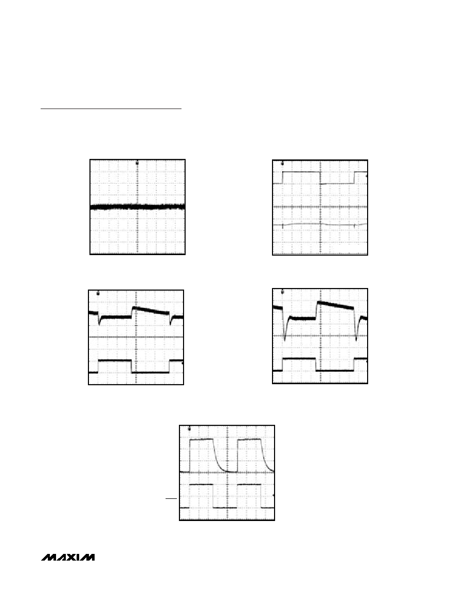
40µs/div
LINE TRANSIENT
V
OUTA
10mV/div
AC-COUPLED
MAX8559 toc11
V
INA
4.5V
3.5V
1V/div
I
OUTA
= 100mA
10µs/div
LOAD TRANSIENT
I
OUTA
100mA/div
MAX8559 toc12
V
OUTA
20mV/div
AC-COUPLED
0
MAX8559
Dual, 300mA, Low-Noise Linear Regulator
with Independent Shutdown in UCSP or TDFN
_______________________________________________________________________________________
5
10µs/div
LOAD TRANSIENT
NEAR DROPOUT
I
OUTA
100mA/div
MAX8559 toc13
V
OUTA
20mV/div
AC-COUPLED
0
1ms/div
SHUTDOWN RESPONSE
V
SHDNA
1V/div
MAX8559 toc14
V
OUTA
1V/div
0
0
Typical Operating Characteristics (continued)
(V
OUTA
= V
OUTB
= 2.85V, V
INA
= V
INB
= 3.8V, C
OUT
= 2.2µF (or 4.7µF for 300mA), C
BP
= 0.01µF, and C
IN
= 2.2µF (or 4.7µF for
300mA), unless otherwise noted.)
1ms/div
OUTPUT NOISE
(10Hz to 100kHz)
V
OUT_
500µV/div
MAX8559 toc10