General Description
The MAX8568A/MAX8568B backup-battery-management
ICs are complete charging and backup switchover con-
trol solutions for PDAs, Smart Phones, and other smart
portable devices. They charge both NiMH and
rechargeable lithium battery types and feature pro-
grammable charge current and termination voltage.
Separate optimized charge algorithms for both lithium
and NiMH cells are included on-chip.
The MAX8568A/MAX8568B also manage backup
switchover from a primary power source. An accurate on-
chip voltage detector monitors the main supply and
backs up two system supplies (typically I/O and memory)
when main power falls. On-chip drivers switch external
MOSFETs to disconnect the main supply from the system
loads so the backup source is not drained.
Low-voltage backup cells can be stepped up by an on-
chip synchronous-rectified, low-quiescent-current boost
converter. Additionally, a low-quiescent-current LDO gen-
erates a second backup voltage. The MAX8568A LDO is
preset to 2.5V while the MAX8568B LDO is preset to 1.8V.
Both devices are supplied in 16-pin 3mm x 3mm thin
QFN packages rated for -40∞C to +85∞C operation.
Applications
PDAs and PDA Phones
Smart Phones
DSCs and DVCs
Palmtops and Wireless Handhelds
Internet Appliances and Web-Books
Features
Automatically Manage All Backup Switchover
Functions
Charge Both NiMH and Rechargeable Lithium
Backup Batteries
On-Chip Battery Boost Converter for 1-Cell NiMH
Two Backup Output Voltages
Programmable Charge Current
Programmable Charge Voltage Limit
Low 17µA Operating Current in Backup Mode
Eliminate Many Discrete Components
Tiny 3mm x 3mm Thin QFN Package
MAX8568A/MAX8568B
Complete Backup-Management ICs
for Lithium and NiMH Batteries
________________________________________________________________ Maxim Integrated Products
1
12
13
14
15
16
8
7
6
5
11
10
9
1
2
3
4
CHGI
INOK
BKV
NI/LI
OD2
OD1
LDO
BKSU
STRTV
TERMV
REF
IN
BK
PGND
LX
GND
TOP VIEW
MAX8568A
MAX8568B
THIN QFN
Pin Configuration
Ordering Information
MAX8568A
MAX8568B
IN
BK
LX
BKSU
PGND
BKV
OD1
LDO
OD2
REF
TERMV
STRTV
GND
INOK
NI/LI
CHGI
NI
LI
IN
MAIN BATTERY
2.8V TO 5.5V
BACKUP
BATTERY
I/O OUT
3.3V, 50mA
I/O IN
MEM OUT
1.8V OR 2.5V, 10mA
MEM IN
Typical Operating Circuit
19-3450; Rev 0; 11/04
For pricing, delivery, and ordering information, please contact Maxim/Dallas Direct! at
1-888-629-4642, or visit Maxim's website at www.maxim-ic.com.
EVALUATION KIT
AVAILABLE
PART
TEMP RANGE
PIN-
PACKAGE
TOP
MARK
MAX8568AETE
-40∞C to +85∞C
16 Thin QFN
3mm x 3mm
(T1633-4)
ACK
MAX8568BETE
-40∞C to +85∞C
16 Thin QFN
3mm x 3mm
(T1633-4)
ACL

MAX8568A/MAX8568B
Complete Backup-Management ICs
for Lithium and NiMH Batteries
2
_______________________________________________________________________________________
ABSOLUTE MAXIMUM RATINGS
ELECTRICAL CHARACTERISTICS
(Circuit of Figure 7, V
IN
= V
INOK
= 3.6V, V
BK
= 1.4V, V
NI/LI
= V
BKSU
= 3.3V, V
BKV
= GND = PGND = 0V, V
STRTV
= V
TERMV
= 1.2V,
R5 = 250k
, T
A
= 0∞C to +85∞C, unless otherwise noted. Typical values are at T
A
= +25∞C.) (Note 1)
Stresses beyond those listed under "Absolute Maximum Ratings" may cause permanent damage to the device. These are stress ratings only, and functional
operation of the device at these or any other conditions beyond those indicated in the operational sections of the specifications is not implied. Exposure to
absolute maximum rating conditions for extended periods may affect device reliability.
IN, BK, BKSU, OD1, OD2 to GND.........................-0.3V to +6.0V
BKV, LDO, NI/LI to GND.........................-0.3V to (V
BKSU
+ 0.3V)
REF, CHGI, INOK, TERMV, STRTV to GND...-0.3V to (V
IN
+ 0.3V)
PGND to GND ......................................................-0.3V to + 0.3V
LX Current ......................................................................0.9A
RMS
Continuous Power Dissipation (T
A
= +70∞C)
16-Pin 3mm x 3mm Thin QFN
(derate 15.6mW/∞C above +70∞C) .............................1250mW
Operating Temperature Range ...........................-40∞C to +85∞C
Junction Temperature ......................................................+150∞C
Storage Temperature Range .............................-65∞C to +150∞C
Lead Temperature (soldering, 10s) .................................+300∞C
PARAMETER
CONDITIONS
MIN
TYP
MAX
UNITS
IN Voltage Range
2.8
5.5
V
T
A
= +25∞C
3
5
Charger off, V
INOK
= 1.5V
T
A
= +85∞C
3
IN Operating Current
Charger on, not including charge current
50
90
µA
CHGI Current Limit
R
CHGI
= 169k
, V
BK
= 1.3V
8
10
12
mA
CHGI Bias Voltage
600
mV
CHGI Resistor Range
V
BK
= 1.3V
50
1800
k
V
IN
= 5.5V, V
NI/LI
= 0V
4.116
4.2
4.284
V
IN
= 3.8V, V
NI/LI
= 0V, V
TERMV
= 1V
3.42
3.5
3.58
BK Charge Voltage Limit
V
IN
= V
NI/LI
= 3.6V
1.746
1.8
1.854
V
T
A
= +25∞C
0.01
0.5
BK Reverse Leakage Current to IN
V
IN
= 0V
T
A
= +85∞C
0.1
µA
NiMH Mode BK High Threshold Voltage,
V
BK(NIHI)
V
TERMV
= 1.2V
1.37
1.4
1.43
V
NiMH Mode BK Low Threshold Voltage,
V
BK(NILO)
V
STRTV
= 1.2V
1.17
1.2
1.23
V
T
A
= +25∞C
0.001
0.05
TERMV Input Current
V
TERMV
= 1.1V
T
A
= +85∞C
0.01
µA
T
A
= +25∞C
0.001
0.05
STRTV Input Current
V
STRTV
= 1.1V
T
A
= +85∞C
0.01
µA
REF Output Voltage
I
REF
= 1µA
1.23
1.25
1.27
V
REF Load Regulation
I
REF
= 1µA to 50µA
2.5
10
mV
REF Line Regulation
V
IN
= 3V to 5.5V, I
REF
= 1µA
1
7
mV
V
INOK
falling
2.38
2.43
2.48
INOK Threshold Voltage
V
INOK
rising
2.40
2.47
2.54
V
T
A
= +25∞C
0.005
0.1
INOK Input Current
V
INOK
= 2V
T
A
= +85∞C
0.05
µA
NI/LI Logic-Level High
V
BKSU
= 3.3V
1.8
V
NI/LI Logic-Level Low
V
BKSU
= 3.3V
0.4
V
MAX8568A/MAX8568B
Complete Backup-Management ICs
for Lithium and NiMH Batteries
_______________________________________________________________________________________
3
ELECTRICAL CHARACTERISTICS (continued)
(Circuit of Figure 7, V
IN
= V
INOK
= 3.6V, V
BK
= 1.4V, V
NI/LI
= V
BKSU
= 3.3V, V
BKV
= GND = PGND = 0V, V
STRTV
= V
TERMV
= 1.2V,
R5 = 250k
, T
A
= 0∞C to +85∞C, unless otherwise noted. Typical values are at T
A
= +25∞C.) (Note 1)
PARAMETER
CONDITIONS
MIN
TYP
MAX
UNITS
T
A
= +25∞C
0.05
1
NI/LI Input Current
V
BKSU
= V
NI/LI
= 3.3V
T
A
= +85∞C
0.1
µA
OD_ On-Resistance
V
BKSU
= 3.6V
11
30
T
A
= +25∞C
0.01
1
OD_ Leakage Current
V
OD_
= 5.5V
T
A
= +85∞C
0.1
µA
BACKUP STEP-UP (Note 2)
V
NI/LI
= 0V, falling trip point
2.45
BK Input Undervoltage Lockout
V
NI/LI
= V
BKSU
= 3.3V, falling trip point
1.05
1.12
1.21
V
BK Input Voltage
5.5
V
Quiescent Current into BKSU
I
LDO
= 0mA, not switching
17
25
µA
Quiescent Current into BK
I
BKSU
= I
LDO
= 0mA, not switching
2.4
4
µA
T
A
= +25∞C
0.001
0.5
Shutdown Current into BK
V
IN
= V
INOK
= V
BKSU
= 0V
T
A
= +85∞C
0.1
µA
BKV Feedback Voltage
1.162
1.21
1.258
V
T
A
= +25∞C
5
50
BKV Feedback Bias Current
V
BKV
= 1V
T
A
= +85∞C
10
nA
V
BKV
= 0V
3.17
3.3
3.43
BKSU Output-Voltage Accuracy
V
BKV
= V
BKSU
2.4
2.5
2.6
V
BKSU Output Voltage Range
2.5
5
V
n-Channel Switch On-Resistance
I
LX
= 200mA
0.4
1
p-Channel Switch On-Resistance
I
LX
= 200mA
0.7
2
T
A
= +25∞C
0.05
1
LX Leakage Current
T
A
= +85∞C
0.1
µA
LX Current Limit (ILIM)
400
500
600
mA
n-Channel Switch Maximum On-Time
3.5
5
6.5
µs
p-Channel Zero-Channel Crossing Current
5
20
35
mA
LOW-DROPOUT REGULATOR
BKSU Input Voltage Range
2.7
5.0
V
MAX8568A
2.375
2.5
2.625
LDO Output-Voltage Accuracy
V
BKSU
= 3.3V
MAX8568B
1.71
1.8
1.89
V
LDO Line Regulation
2.7V < V
BKSU
< 5V, I
LDO
= 1mA
1
mV
LDO Load Regulation
1µA < I
LDO
< 10mA
2.5
mV
MAX8568A/MAX8568B
Complete Backup-Management ICs
for Lithium and NiMH Batteries
4
_______________________________________________________________________________________
ELECTRICAL CHARACTERISTICS
(Circuit of Figure 7, V
IN
= V
INOK
= 3.6V, V
BK
= 1.4V, V
NI/LI
= V
BKSU
= 3.3V, V
BKV
= GND = PGND = 0V, V
STRTV
= V
TERMV
= 1.2V,
R5 = 250k
, T
A
= -40∞C to +85∞C, unless otherwise noted. Typical values are at T
A
= +25∞C.) (Note 3)
PARAMETER
CONDITIONS
MIN
MAX
UNITS
IN Voltage Range
2.8
5.5
V
IN Operating Current
Charger on, not including charge current
90
µA
CHGI Current Limit
R
CHGI
= 169k
, V
BK
= 1.3V
8
12
mA
CHGI Resistor Range
V
BK
= 1.3V
50
1800
k
V
IN
= 5.5V, V
NI/LI
= 0V
4.116
4.310
V
IN
= 3.8V, V
NI/LI
= 0V, V
TERMV
= 1V
3.420
3.605
BK Charge Voltage Limit
V
IN
= V
NI/LI
= 3.6V
1.746
1.854
V
NiMH Mode BK High Threshold Voltage,
V
BK(NIHI)
V
TERMV
= 1.2V
1.37
1.43
V
NiMH Mode BK Low Threshold Voltage,
V
BK(NILO)
V
STRTV
= 1.2V
1.17
1.23
V
REF Output Voltage
I
REF
= 1µA
1.225
1.275
V
REF Load Regulation
I
REF
= 1µA to 50µA
10
mV
REF Line Regulation
V
IN
= 3V to 5.5V, I
REF
= 1µA
7
mV
V
INOK
falling
2.38
2.48
INOK Threshold Voltage
V
INOK
rising
2.40
2.54
V
NI/LI Logic-Level High
V
BKSU
= 3.3V
1.8
V
NI/LI Logic-Level Low
V
BKSU
= 3.3V
0.4
V
OD_ On-Resistance
V
BKSU
= 3.6V
30
BACKUP STEP-UP (Note 2)
BK Input Undervoltage Lockout
V
NI/LI
= V
BKSU
= 3.3V, falling trip point
1.05
1.21
V
BK Input Voltage
5.5
V
Quiescent Current into BKSU
I
LDO
= 0mA, not switching
25
µA
Quiescent Current into BK
I
BKSU
= I
LDO
= 0mA, not switching
4
µA
BKV Feedback Voltage
1.162
1.258
V
V
BKV
= 0V
3.17
3.43
BKSU Output-Voltage Accuracy
V
BKV
= V
BKSU
2.4
2.6
V
BKSU Output Voltage Range
2.5
5.0
V
n-Channel Switch On-Resistance
I
LX
= 200mA
1
p-Channel Switch On-Resistance
I
LX
= 200mA
2
MAX8568A/MAX8568B
Complete Backup-Management ICs
for Lithium and NiMH Batteries
_______________________________________________________________________________________
5
ELECTRICAL CHARACTERISTICS (continued)
(Circuit of Figure 7, V
IN
= V
INOK
= 3.6V, V
BK
= 1.4V, V
NI/LI
= V
BKSU
= 3.3V, V
BKV
= GND = PGND = 0V, V
STRTV
= V
TERMV
= 1.2V,
R5 = 250k
, T
A
= -40∞C to +85∞C, unless otherwise noted. Typical values are at T
A
= +25∞C.) (Note 3)
PARAMETER
CONDITIONS
MIN
MAX
UNITS
LX Current Limit (ILIM)
400
600
mA
n-Channel Switch Maximum On-Time
3.5
6.5
µs
p-Channel Zero-Channel Crossing Current
5
35
mA
LOW-DROPOUT REGULATOR
BKSU Input Voltage Range
2.7
5.0
V
MAX8568A
2.375
2.625
LDO Output-Voltage Accuracy
V
BKSU
= 3.3V
MAX8568B
1.71
1.89
V
Note 1: All units are 100% production tested at T
A
= +25∞C. Limits over the operating range are guaranteed by design.
Note 2: All backup step-up converter specifications are with V
IN
= V
INOK
= 0V, unless otherwise noted.
Note 3: Specifications to -40∞C are guaranteed by design and not production tested.
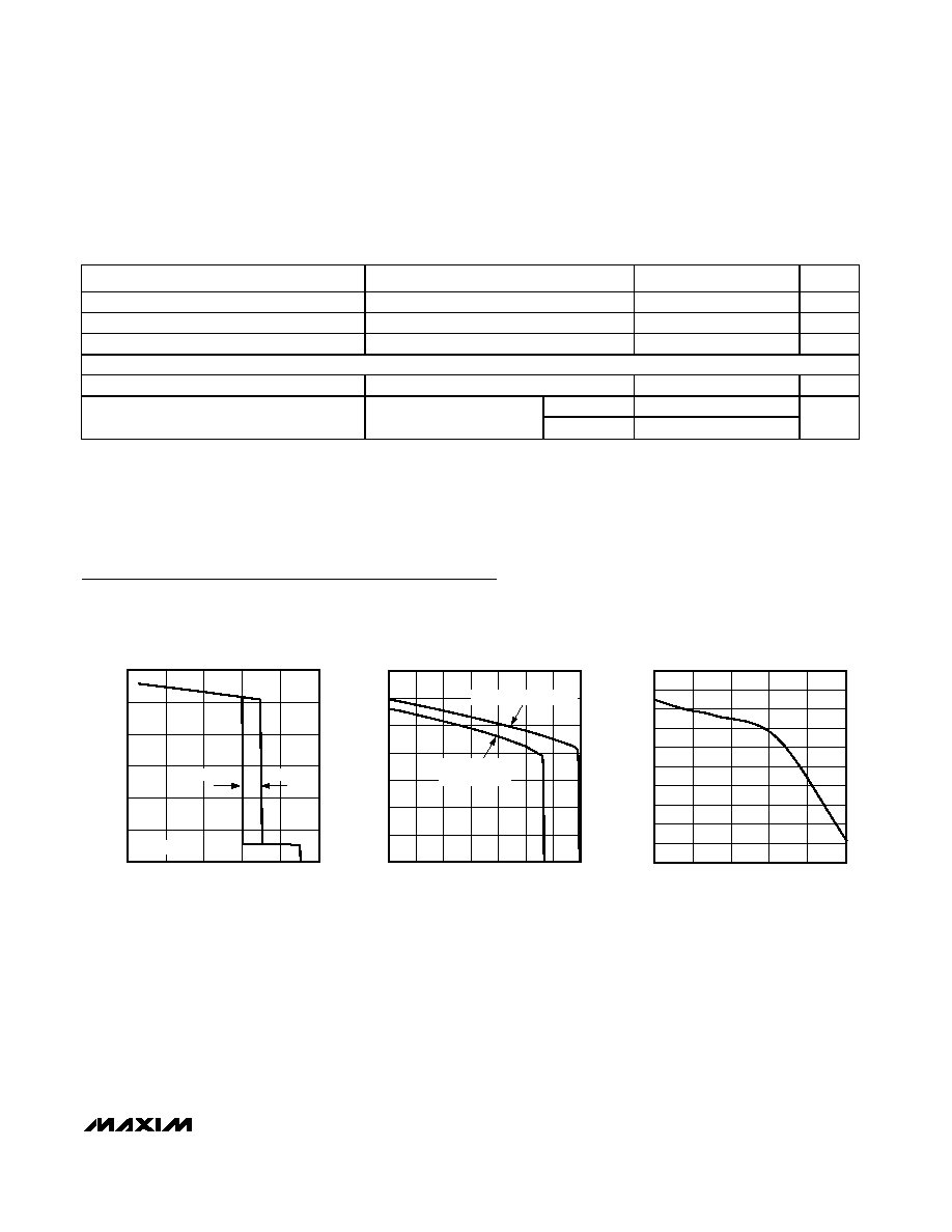
Typical Operating Characteristics
(Circuit of Figure 7, V
IN
= 3.6V, V
BK
= 1.4V, V
NI/LI
= V
BKSU
= 3.3V, T
A
= +25∞C, unless otherwise noted.)
NiMH CHARGE CURRENT
vs. BACKUP BATTERY VOLTAGE
MAX8568 toc01
BACKUP BATTERY VOLTAGE (V)
CHARGE CURRENT (mA)
1.6
1.2
0.8
0.4
2
4
6
8
10
12
0
0
2.0
V
IN
= 3.9V
FALLING
RISING
LITHIUM CHARGE CURRENT
vs. BACKUP BATTERY VOLTAGE
MAX8568 toc02
BACKUP BATTERY VOLTAGE (V)
LITHIUM CHARGE CURRENT (mA)
3.6
3.0
2.4
1.8
1.2
0.6
0
4.2
2
4
6
8
10
14
12
0
V
IN
= 3.9V
V
BK(LIMAX)
= 3.4V
V
IN
= 5V, V
BK(LIMAX)
= 4.2V
Li-ION TERMINATION VOLTAGE
vs. TEMPERATURE
MAX8568 toc03
TEMPERATURE (
∞C)
TERMINATION VOLTAGE (V)
60
35
10
-15
4.171
4.172
4.173
4.174
4.175
4.176
4.177
4.178
4.179
4.180
4.170
-40
85