 | –≠–ª–µ–∫—Ç—Ä–æ–Ω–Ω—ã–π –∫–æ–º–ø–æ–Ω–µ–Ω—Ç: MAX860ESA | –°–∫–∞—á–∞—Ç—å:  PDF PDF  ZIP ZIP |
_______________General Description
The MAX860/MAX861 charge-pump voltage converters
invert input voltages ranging from +1.5V to +5.5V, or
double input voltages ranging from +2.5V to +5.5V.
Because of their high switching frequencies, these
devices use only two small, low-cost capacitors. Their
50mA output makes switching regulators unnecessary,
eliminating inductors and their associated cost, size,
and EMI. Greater than 90% efficiency over most of the
load-current range, combined with a typical operating
current of only 200µA (MAX860), provides ideal perfor-
mance for both battery-powered and board-level volt-
age-conversion applications.
A frequency-control (FC) pin provides three switching-
frequencies to optimize capacitor size and quiescent
current and to prevent interference with sensitive cir-
cuitry. Each device has a unique set of three available
frequencies. A shutdown (S
--
H
--
D
--
N
≠
) pin reduces current
consumption to less than 1µA. The MAX860/MAX861
are suitable for use in applications where the ICL7660
and MAX660's switching frequencies are too low. The
MAX860/MAX861 are available in 8-pin µMAX and
SO packages.
________________________Applications
Portable Computers
Medical Instruments
Interface Power Supplies
Hand-Held Instruments
Operational-Amplifier Power Supplies
____________________________Features
o
8-Pin, 1.11mm High µMAX Package
o
Invert or Double the Input Supply Voltage
o
Three Selectable Switching Frequencies
o
High Frequency Reduces Capacitor Size
o
87% Efficiency at 50mA
o
200µA Quiescent Current (MAX860)
o
1µA Shutdown Supply Current
o
600mV Voltage Drop at 50mA Load
o
12
Output Resistance
______________Ordering Information
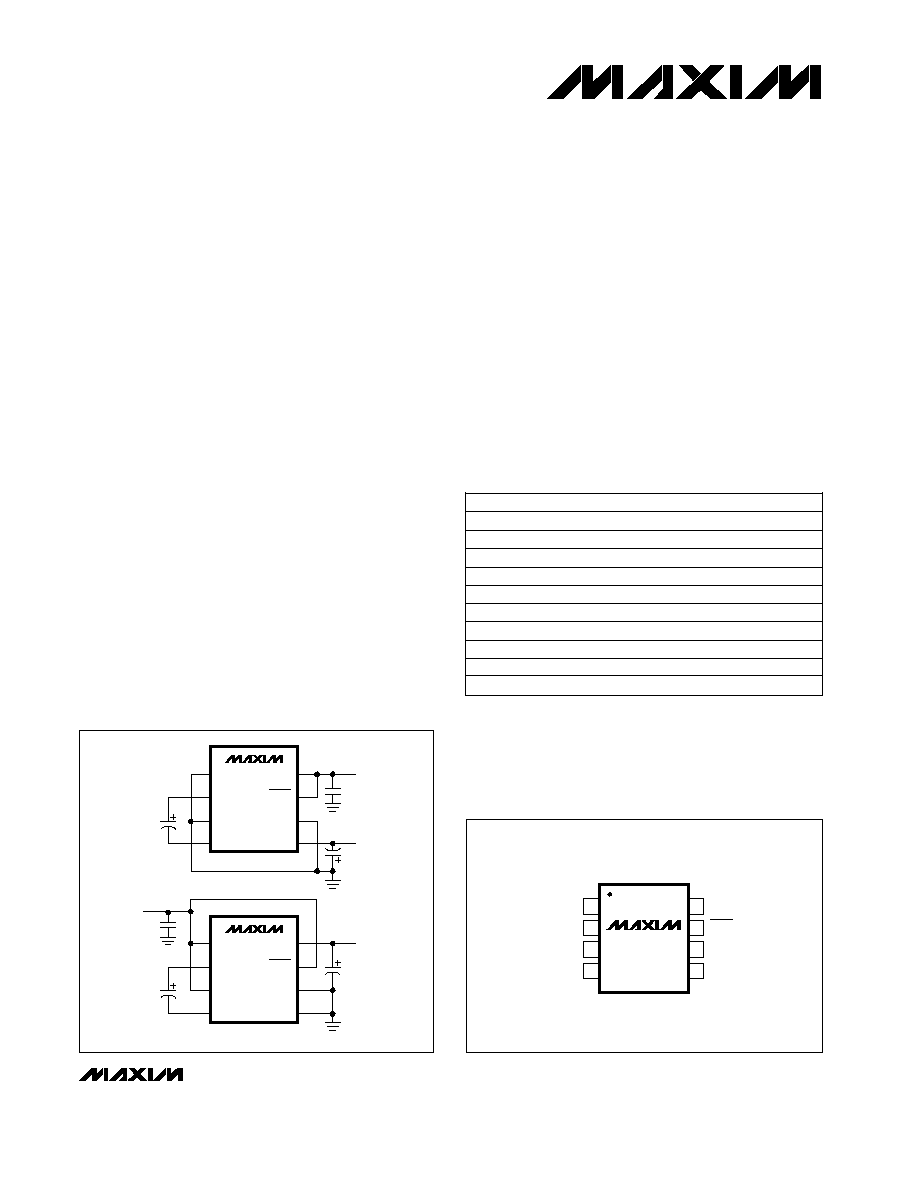
MAX860/MAX861
50mA, Frequency-Selectable,
Switched-Capacitor Voltage Converters
________________________________________________________________
Maxim Integrated Products
1
1
2
3
4
8
7
6
5
V
DD
SHDN
LV
OUT
C1-
GND
C1+
FC
MAX860
MAX861
SO/
µ
MAX
TOP VIEW
__________________Pin Configuration
1
2
3
4
8
7
6
5
FC
C1+
GND
C1-
OUT
LV
SHDN
V
DD
MAX860
MAX861
1
2
3
4
8
7
6
5
FC
C1+
GND
C1-
OUT
LV
SHDN
V
DD
MAX860
MAX861
INPUT
VOLTAGE
+1.5V TO +5.5V
INVERTED
NEGATIVE
OUTPUT
INPUT
VOLTAGE
+2.5V TO +5.5V
DOUBLED
POSITIVE
OUTPUT
10
µ
F
10
µ
F
10
µ
F
10
µ
F
C1
C1
C2
C2
VOLTAGE INVERTER
POSITIVE VOLTAGE DOUBLER
__________Typical Operating Circuit
19-0239; Rev 1; 11/96
PART
MAX860
ISA
MAX860IUA
-25∞C to +85∞C
-25∞C to +85∞C
TEMP. RANGE
PIN-PACKAGE
8 SO
8 µMAX
* Dice are tested at T
A
= +25∞C, DC parameters only.
Contact factory for availability.
MAX860C/D
0∞C to +70∞C
Dice*
MAX860ESA
-40∞C to +85∞C
8 SO
MAX860MJA
-55∞C to +125∞C
8 CERDIP
MAX861
ISA
-25∞C to +85∞C
8 SO
MAX861IUA
-25∞C to +85∞C
8 µMAX
MAX861C/D
0∞C to +70∞C
Dice*
MAX861ESA
-40∞C to +85∞C
8 SO
MAX861MJA
-55∞C to +125∞C
8 CERDIP
For free samples & the latest literature: http://www.maxim-ic.com, or phone 1-800-998-8800
MAX860/MAX861
50mA, Frequency-Selectable,
Switched-Capacitor Voltage Converters
2
_______________________________________________________________________________________
ABSOLUTE MAXIMUM RATINGS
ELECTRICAL CHARACTERISTICS
(Typical Operating Circuit (Inverter), V
DD
= +5V,
≠
S
--
H
--
D
--
N
≠
= V
DD
, FC = LV = GND, C1 = C2 = 10µF (Note 2), T
A
= T
MIN
to T
MAX
, unless
otherwise noted. Typical values are at T
A
= +25∞C.)
Stresses beyond those listed under "Absolute Maximum Ratings" may cause permanent damage to the device. These are stress ratings only, and functional
operation of the device at these or any other conditions beyond those indicated in the operational sections of the specifications is not implied. Exposure to
absolute maximum rating conditions for extended periods may affect device reliability.
Supply Voltage (V
DD
to GND or GND to OUT) ...................+6.0V
Input Voltage Range (LV, FC,
≠
S
--
H
--
D
--
N
≠
) ...................(OUT - 0.3V)
to (V
DD
+ 0.3V)
Continuous Output Current (OUT, V
DD
) .............................60mA
Output Short-Circuit to GND (Note 1)...................................1sec
Continuous Power Dissipation (T
A
= +70∞C)
SO (derate 5.88mW/∞C above +70∞C) .........................471mW
µMAX (derate 4.10mW/∞C above +70∞C) ....................330mW
CERDIP (derate 8.00mW/∞C above +70∞C) .................640mW
Operating Temperature Ranges
MAX86_I_A ......................................................-25∞C to +85∞C
MAX86_ESA.....................................................-40∞C to +85∞C
MAX86_MJA ..................................................-55∞C to +125∞C
Storage Temperature Range .............................-65∞C to +160∞C
Lead Temperature (soldering, 10sec) .............................+300∞C
I
L
= 10mA, V
DD
= 2V
R
L
= 1k
I
L
= 50mA
V
DD
= 3V, V
OUT
more negative than -2.5V
V
DD
= 5V, V
OUT
more negative than -3.75V
MAX861M
MAX860M
MAX861I/E
MAX860I/E
CONDITIONS
20
35
R
OUT
Output Resistance
(Note 3)
12
25
mA
I
OUT
Output Current
50
100
mA
6.5
I
DD
No-Load Supply Current
2.6
0.5
2.5
5.0
1.1
2.0
V
2.5
5.5
V
DD
Supply Voltage
1.5
5.5
0.3
0.4
3.3
1.3
0.4
0.2
0.3
0.07
0.6
1.0
1.4
2.5
UNITS
MIN
TYP
MAX
SYMBOL
PARAMETER
Inverter, LV = GND
Doubler, LV = OUT
FC = V
DD
= 5V
FC = OUT
FC = GND
FC = V
DD
= 3V
FC = V
DD
FC = OUT
FC = GND
FC = V
DD
FC = OUT
FC = GND
FC = V
DD
FC = OUT
FC = GND
10
30
Note 1:
OUT may be shorted to GND for 1sec without damage, but shorting OUT to V
DD
may damage the device and should be
avoided. Also, for temperatures above +85∞C, OUT must not be shorted to GND or V
DD
, even instantaneously, or device
damage may result.
MAX860/MAX861
50mA, Frequency-Selectable,
Switched-Capacitor Voltage Converters
_______________________________________________________________________________________
3
ELECTRICAL CHARACTERISTICS (continued)
(Typical Operating Circuit (Inverter), V
DD
= +5V,
≠
S
--
H
--
D
--
N
≠
= V
DD
, FC = LV = GND, C1 = C2 = 10µF (Note 2), T
A
= T
MIN
to T
MAX
, unless
otherwise noted. Typical values are at T
A
= +25∞C.)
Note 2:
C1 and C2 are low-ESR (<0.2
) aluminum electrolytics. Capacitor ESR adds to the circuit's output resistance. Using
capacitors with higher ESR may reduce output voltage and efficiency.
Note 3:
Specified output resistance includes the effect of the 0.2
ESR of the test circuit's capacitors.
Note 4:
The switches are driven directly at the oscillator frequency, without any division.
Note 5:
At lowest frequencies, using 10µF capacitors gives worse efficiency figures than using the recommended capacitor
values in Table 3, due to larger 1 / (f
s
x C1) term in R
OUT
.
≠
S
--
H
--
D
--
N
≠
< 0.3V
MAX860
LV = GND
No load
MAX860/MAX861, FC = V
DD
,
I
L
= 50mA to GND, C1 = C2 = 68µF
MAX860,
FC = V
DD
MAX861,
FC = V
DD
MAX861
FC < 4V
CONDITIONS
µA
10
Shutdown Supply Current
1
V
0.3
V
IL
≠
S
--
H
--
D
--
N
≠
Threshold
1.2
V
IH
%
99
99.9
Voltage-Conversion Efficiency
%
87
Power Efficiency (Note 5)
88
92
93
96
80
130
30
50
3
6
90
93
93
96
8
13
60
100
kHz
160
250
f
S
Switching Frequency
(Note 4)
µA
-2
-4
I
FC
FC Current (from V
DD
)
UNITS
MIN
TYP
MAX
SYMBOL
PARAMETER
No load, V
OUT
= -4V
µs
500
Time to Exit Shutdown
FC = V
DD
FC = GND
FC = OUT
FC = V
DD
FC = GND
FC = OUT
R
L
= 2k
from V
DD
to OUT
R
L
= 1k
from OUT
to GND
R
L
= 2k
from V
DD
to OUT
R
L
= 1k
from OUT
to GND
MAX86_I/E
MAX86_M
MAX860/MAX861
50mA, Frequency-Selectable,
Switched-Capacitor Voltage Converters
4
_______________________________________________________________________________________
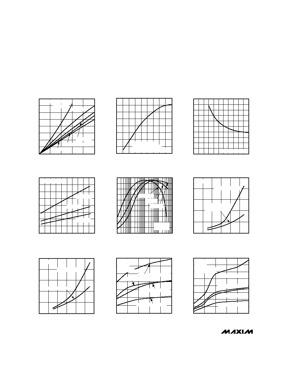
__________________________________________Typical Operating Characteristics
(All curves generated using the inverter circuit shown in the
Typical Operating Circuits with LV = GND and T
A
= +25∞C, unless other-
wise noted. Test results also valid for doubler mode with LV = OUT and T
A
= +25∞C. All capacitor values used are those recom-
mended in Table 3, unless otherwise noted. The output resistance curves represent the resistance of the device itself, which is R
O
in
the equation for R
OUT
shown in the
Capacitor Selection section.)
0.7
0
0
OUTPUT VOLTAGE DROP FROM
SUPPLY VOLTAGE vs. LOAD CURRENT
0.8
MAX860-01
LOAD CURRENT (mA)
V
OUT
DROP (V)
30
0.4
0.2
10
20
50
0.6
40
0.1
0.3
0.5
V
DD
= +1.5V
V
DD
= +2.5V
V
DD
= +3.5V
V
DD
= +4.5V, +5.0V
V
DD
= +5.5V
ALL FREQUENCIES
2
-14
1.5 2.0
3.0
4.0
OSCILLATOR FREQUENCY vs.
SUPPLY VOLTAGE
-6
0
MAX860-02
SUPPLY VOLTAGE (V)
PERCENTAGE FREQUENCY CHANGE (
%
)
(FROM FREQUENCY MEASURED WITH V
DD
= +5V)
2.5
3.5
-2
-4
4.5 5.0 5.5
-8
-10
-12
ALL FREQUENCIES,
LV CONNECTED TO GND
(INVERTER) OR OUT (DOUBLER)
1.0
20
0
0
1
3
5
OUTPUT SOURCE RESISTANCE (R
O
) vs.
SUPPLY VOLTAGE
4
16
MAX860-03
SUPPLY VOLTAGE (V)
OUTPUT SOURCE RESISTANCE (
)
2
4
12
8
2
6
10
14
18
ALL FREQUENCIES
32
0
-60
-20
40
140
OUTPUT SOURCE RESISTANCE (R
O
) vs.
TEMPERATURE
8
28
MAX860-04
TEMPERATURE (∞C)
OUTPUT SOURCE RESISTANCE (
)
20
100
24
16
-40
0
60 80
120
20
12
4
V
DD
= +3V
V
DD
= +5V
V
DD
= +1.5V
ALL FREQUENCIES
0
0
MAX861 SUPPLY CURRENT
vs. SUPPLY VOLTAGE
MAX860-07
SUPPLY VOLTAGE (V)
SUPPLY CURRENT (
µ
A)
100
200
300
500
1
2
3
4
5
6
400
DOUBLER, LV = OUT
INVERTER, LV = GND
FC = V
DD
100
0
0.01
1
100
MAX860
EFFICIENCY vs. LOAD CURRENT
20
MAX860-05
LOAD CURRENT (mA)
EFFICIENCY (%)
40
60
80
10
30
50
70
90
0.1
10
INVERTER
FC = V
DD
V
DD
= +1.5V
V
DD
= +3V
V
DD
= +5V
0
0
MAX860 SUPPLY CURRENT
vs. SUPPLY VOLTAGE
MAX860-06
SUPPLY VOLTAGE (V)
SUPPLY CURRENT (
µ
A)
100
200
300
500
1
2
3
4
5
6
400
DOUBLER, LV = OUT
INVERTER, LV = GND
(V
DD
> 3V)
FC = V
DD
70
0
0.33
MAX860 OUTPUT CURRENT vs. CAPACITANCE
HIGH-FREQUENCY MODE
MAX860-08
CAPACITANCE (
µ
F)
OUTPUT CURRENT (mA)
4.7
40
20
1
2.2
22
60
10
10
30
50
V
IN
= +4.5V, V
OUT
= -3.5V
V
IN
= +4.5V, V
OUT
= -4V
V
IN
= +3V, V
OUT
= -2.4V
V
IN
= +3V, V
OUT
= -2.7V
f
OSC
= 130kHz
FC = OUT
LV = GND
INVERTER MODE
80
70
0
0.33
MAX860 OUTPUT CURRENT vs. CAPACITANCE
MEDIUM-FREQUENCY MODE
MAX860-09
CAPACITANCE (
µ
F)
OUTPUT CURRENT (mA)
4.7
40
20
1
2.2
22
60
10
10
30
50
V
IN
= +4.5V, V
OUT
= -3.5V
V
IN
= +3V, V
OUT
= -2.4V
V
IN
= +4.5V, V
OUT
= -4V
V
IN
= +3V, V
OUT
= -2.7V
f
OSC
= 50kHz
FC = GND
LV = GND
INVERTER MODE

MAX860/MAX861
50mA, Frequency-Selectable,
Switched-Capacitor Voltage Converters
_______________________________________________________________________________________
5
90
70
80
0
0.33
MAX861
OUTPUT CURRENT vs. CAPACITANCE
HIGH-FREQUENCY MODE
MAX860-10
CAPACITANCE (
µ
F)
OUTPUT CURRENT (mA)
4.7
40
20
1
2.2
22
60
10
10
30
50
V
IN
= +4.5V,
V
OUT
= -3.5V
V
IN
= +4.5V, V
OUT
= -4V
V
IN
= +3V, V
OUT
= -2.4V
V
IN
= +3V, V
OUT
= -2.7V
f
OSC
= 250kHz
FC = OUT
LV = GND
INVERTER MODE
80
70
0
0.33
MAX861
OUTPUT CURRENT vs. CAPACITANCE
MEDIUM-FREQUENCY MODE
MAX860-11
CAPACITANCE (
µ
F)
OUTPUT CURRENT (mA)
4.7
40
20
1
2.2
22
60
10
10
30
50
V
IN
= +4.5V,
V
OUT
= -3.5V
V
IN
= +3V,
V
OUT
= -2.4V
V
IN
= +4.5V,
V
OUT
= -4V
V
IN
= +3V, V
OUT
= -2.7V
f
OSC
= 100kHz
FC = GND
LV = GND
INVERTER MODE
______________________________________________________________Pin Description
____________________________Typical Operating Characteristics (continued)
(All curves generated using the inverter circuit shown in the
Typical Operating Circuits with LV = GND and T
A
= +25∞C, unless other-
wise noted. Test results also valid for doubler mode with LV = OUT and T
A
= +25∞C. All capacitor values used are those recom-
mended in Table 3, unless otherwise noted. The output resistance curves represent the resistance of the device itself, which is R
O
in
the equation for R
OUT
shown in the
Capacitor Selection section.)
INVERTER
DOUBLER
Doubled Positive Output
Flying-Capacitor Negative Terminal
Ground
Low-Voltage-Operation Input. Connect to OUT.
Active-Low Shutdown Input. Connect to GND pin if not
used. Connect to OUT to disable the charge pump.
Positive Input Supply
Flying-Capacitor Positive Terminal
Frequency Control, see Table 1
FUNCTION
Positive Input Supply
V
DD
8
Flying-Capacitor Negative Terminal
C1-
4
Negative Output
OUT
5
Low-Voltage-Operation Input. Connect to GND.
LV
6
Active-Low Shutdown Input. Connect to V
DD
if not
used. Connect to GND to disable the charge pump.
≠
S
--
H
--
D
--
N
≠
7
Ground
GND
3
Flying-Capacitor Positive Terminal
C1+
2
Frequency Control, see Table 1
FC
1
NAME
PIN