Äîêóìåíòàöèÿ è îïèñàíèÿ www.docs.chipfind.ru

General Description
The MAX8614A/MAX8614B dual-output step-up DC-DC
converters generate both a positive and negative sup-
ply voltage that are each independently regulated. The
positive output delivers up to 50mA while the inverter
supplies up to 100mA with input voltages between 2.7V
and 5.5V. The MAX8614A/MAX8614B are ideal for pow-
ering CCD imaging devices and displays in digital
cameras and other portable equipment.
The MAX8614A/MAX8614B generate an adjustable
positive output voltage up to +24V and a negative out-
put down to 16V below the input voltage. The
MAX8614B has a higher current limit than the
MAX8614A. Both devices operate at a fixed 1MHz fre-
quency to ease noise filtering in sensitive applications
and to reduce external component size.
Additional features include pin-selectable power-on
sequencing for use with a wide variety of CCDs, True
ShutdownTM, overload protection, fault flag, and internal
soft-start with controlled inrush current.
The MAX8614A/MAX8614B are available in a space-
saving 3mm x 3mm 14-pin TDFN package and
are specified over the -40°C to +85°C extended
temperature range.
Applications
CCD Bias Supplies and OLED Displays
Digital Cameras
Camcorders and Portable Multimedia
PDAs and Smartphones
Features
Dual Output Voltages (+ and -)
Adjustable Up to +24V and Down to -10V at 5.5V
IN
Output Short/Overload Protection
True Shutdown on Both Outputs
Controlled Inrush Current During Soft-Start
Selectable Power-On Sequencing
Up to 90% Efficiency
1µA Shutdown Current
1MHz Fixed-Frequency PWM Operation
Fault-Condition Flag
Thermal Shutdown
Small, 3mm x 3mm, 14-Pin TDFN Package
MAX8614A/MAX8614B
Dual-Output (+ and -) DC-DC
Converters for CCD
________________________________________________________________ Maxim Integrated Products
1
19-4014; Rev 0; 3/06
For pricing, delivery, and ordering information, please contact Maxim/Dallas Direct! at
1-888-629-4642, or visit Maxim's website at www.maxim-ic.com.
14
13
12
11
10
9
8
1
+
2
3
4
5
6
7
LXN
V
CC
PVP
PGND
REF
AV
CC
FBN
ONBST
TOP VIEW
MAX8614A
MAX8614B
LXP
ONINV
SEQ
FBP
FLT
GND
TDFN
Pin Configuration
LXN
V
CC
INPUT
(2.7V TO 5.5V)
REF
AV
CC
AV
CC
FBN
ONINV
V
INV
-7.5V
MAX8614A
MAX8614B
GND
PGND
ONBST
PVP
LXP
FBP
V
BST
+15V
REF
SEQ
FLT
Typical Operating Circuit
Ordering Information
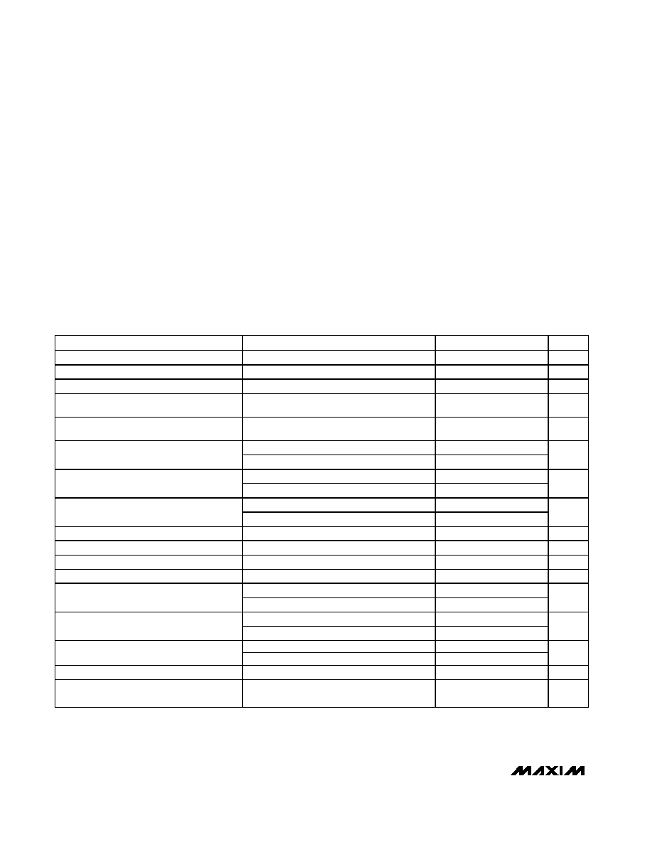
PART
TEMP
RANGE
PIN-
PACKAGE
TOP
MARK
ILIM
BST/INV
MAX8614AETD+
-40°C to
+85°C
14 TDFN
3mm x 3mm
(T1433-2)
ABG
0.44/0.33
MAX8614BETD+
-40°C to
+85°C
14 TDFN
3mm x 3mm
(T1433-2)
ABH
0.8/0.75
True Shutdown is a trademark of Maxim Integrated Products, Inc.
+Denotes lead-free package.
MAX8614A/MAX8614B
Dual-Output (+ and -) DC-DC
Converters for CCD
2
_______________________________________________________________________________________
ABSOLUTE MAXIMUM RATINGS
Stresses beyond those listed under "Absolute Maximum Ratings" may cause permanent damage to the device. These are stress ratings only, and functional
operation of the device at these or any other conditions beyond those indicated in the operational sections of the specifications is not implied. Exposure to
absolute maximum rating conditions for extended periods may affect device reliability.
V
CC
, AV
CC
to GND ...................................................-0.3V to +6V
LXN to V
CC
.............................................................-18V to +0.3V
LXP to PGND ..........................................................-0.3V to +33V
REF, ONINV, ONBST, SEQ, FBN, FBP
FLT to GND ..........................................-0.3V to (AV
CC
+ 0.3)V
PVP to GND ................................................-0.3V to (V
CC
+ 0.3)V
AV
CC
to V
CC
..........................................................-0.3V to +0.3V
PGND to GND .......................................................-0.3V to +0.3V
Continuous Power Dissipation (T
A
= +70°C Multilayer Board)
14-Pin 3mm x 3mm TDFN (derate 18.2mW/°C above
T
A
= +70°C) ............................................................1454.4mW
Operating Temperature Range ...........................-40°C to +85°C
Junction Temperature ......................................................+150°C
Storage Temperature Range .............................-65°C to +150°C
Lead Temperature (soldering, 10s) .................................+300°C
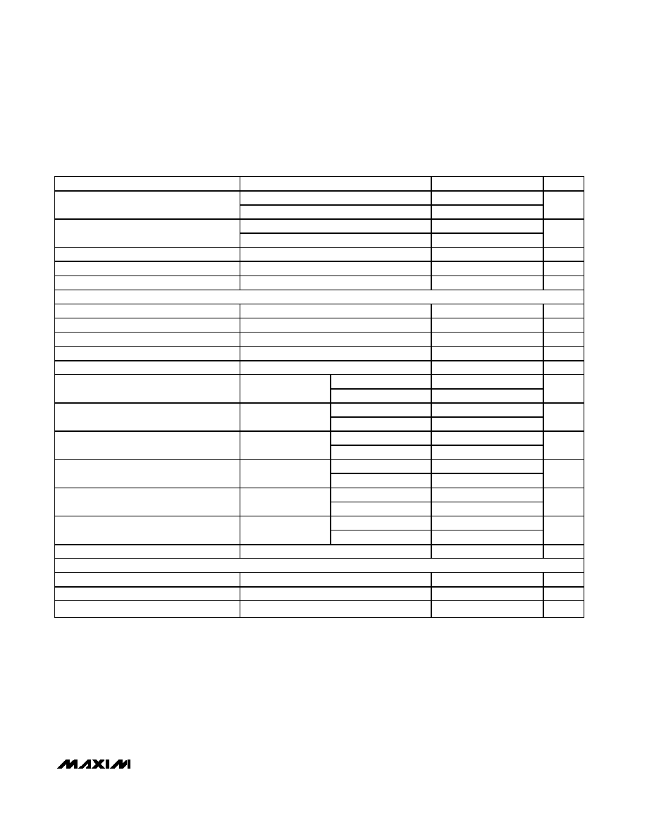
ELECTRICAL CHARACTERISTICS
(V
CC
= V
AVCC
= V
ONINV =
V
ONBST
= 3.6V, PGND = SEQ = GND, C6 = 0.22µF, C1 = 2.2µF, C2 = 4.7µF, Figure 1, T
A
= 0°C to +85°C,
unless otherwise noted. Typical values are at T
A
= +25°C.)
PARAMETER
CONDITIONS
MIN
TYP
MAX
UNITS
AV
CC
and V
CC
Voltage Range
(Note 1)
2.7
5.5
V
UVLO Threshold
V
CC
rising
2.42
2.55
2.66
V
UVLO Hysteresis
25
mV
Step-Up Output Voltage Adjust Range
V
AVCC
24
V
Inverter Output Voltage Adjust Range
V
INV
- V
CC
(Note 2)
-16
0
V
MAX8614B
0.7
0.8
0.9
LXP Current Limit
MAX8614A
0.34
0.44
0.52
A
MAX8614B
0.90
1.05
1.20
LXP Short-Circuit Current Limit
MAX8614A
0.52
0.61
0.70
A
MAX8614B
0.65
0.75
0.85
LXN Current Limit
MAX8614A
0.28
0.33
0.38
A
LXN On-Resistance
V
CC
= 3.6V
0.6
1.1
LXP On-Resistance
V
CC
= 3.6V
0.625
PVP On-Resistance
V
CC
= 3.6V
0.15
0.3
Maximum Duty Cycle
Step-up and inverter
82
90
%
I
AVCC
0.75
1.4
Quiescent Current (Switching, No Load)
I
VCC
2
3
mA
I
AVCC
400
800
Quiescent Current (No Switching, No Load)
IV
CC
8
15
µA
T
A
= +25°C
0.1
5
Shutdown Supply Current
T
A
= +85°C
0.1
µA
FBP Line Regulation
V
CC
= 2.7V to 5.5V
-20
mV/D
FBN Line Regulation
V
CC
= 2.7V to 5.5V
20
mV/
(D - 0.5)
MAX8614A/MAX8614B
Dual-Output (+ and -) DC-DC
Converters for CCD
_______________________________________________________________________________________
3
ELECTRICAL CHARACTERISTICS (continued)
(V
CC
= V
AVCC
= V
ONINV =
V
ONBST
= 3.6V, PGND = SEQ = GND, C6 = 0.22µF, C1 = 2.2µF, C2 = 4.7µF, Figure 1, T
A
= 0°C to +85°C,
unless otherwise noted. Typical values are at T
A
= +25°C.)
PARAMETER
CONDITIONS
MIN
TYP
MAX
UNITS
I
LXP
= I
ILIMMIN
, MAX8614B
-15
FBP Load Regulation
I
LXP
= I
ILIMMIN
, MAX8614A
-35
mV/A
I
LXN
= I
ILIMMIN
, MAX8614B
17.5
FBN Load Regulation
I
LXN
= I
ILIMMIN
, MAX8614A
65
mV/A
Oscillator Frequency
0.93
1
1.07
MHz
Soft-Start Interval
Step-up and inverter
10
ms
Overload-Protection Fault Delay
100
ms
FBP, FBN, REFERENCE
REF Output Voltage
No load
1.24
1.25
1.26
V
REF Load Regulation
0µA < I
REF
< 50µA
10
mV
REF Line Regulation
3.3V < V
AVCC
< 5.5V
2
5
mV
FBP Threshold Voltage
No load
0.995
1.010
1.025
V
FBN Threshold Voltage
No load
-10
0
+10
mV
T
A
= +25°C
-50
+5
+50
FBP Input Leakage Current
V
FBP
=1.025V
T
A
= +85°C
+5
nA
T
A
= +25°C
-50
+5
+50
FBN Input Leakage Current
FBN = -10mV
T
A
= +85°C
+5
nA
T
A
= +25°C
-5
+0.1
+5
LXN Input Leakage Current
V
LXN
= -12V
T
A
= +85°C
+0.1
µA
T
A
= +25°C
-5
+0.1
+5
LXP Input Leakage Current
V
LXP
= 23V
T
A
= +85°C
+0.1
µA
T
A
= +25°C
-5
+0.1
+5
PVP Input Leakage Current
V
PVP
= 0V
T
A
= +85°C
+0.1
µA
T
A
= +25°C
-1
+0.1
+1
FLT Input Leakage Current
V
FLT
= 3.6V
T
A
= +85°C
+0.1
µA
FLT Input Resistance
Fault mode, T
A
= +25°C
10
20
ONINV, ONBST, SEQ LOGIC INPUTS
Logic-Low Input
2.7V < V
AVCC
< 5.5V
0.5
V
Logic-High Input
2.7V < V
AVCC
< 5.5V
1.6
V
Bias Current
T
A
= +25°C
0.1
1
µA
MAX8614A/MAX8614B
Dual-Output (+ and -) DC-DC
Converters for CCD
4
_______________________________________________________________________________________
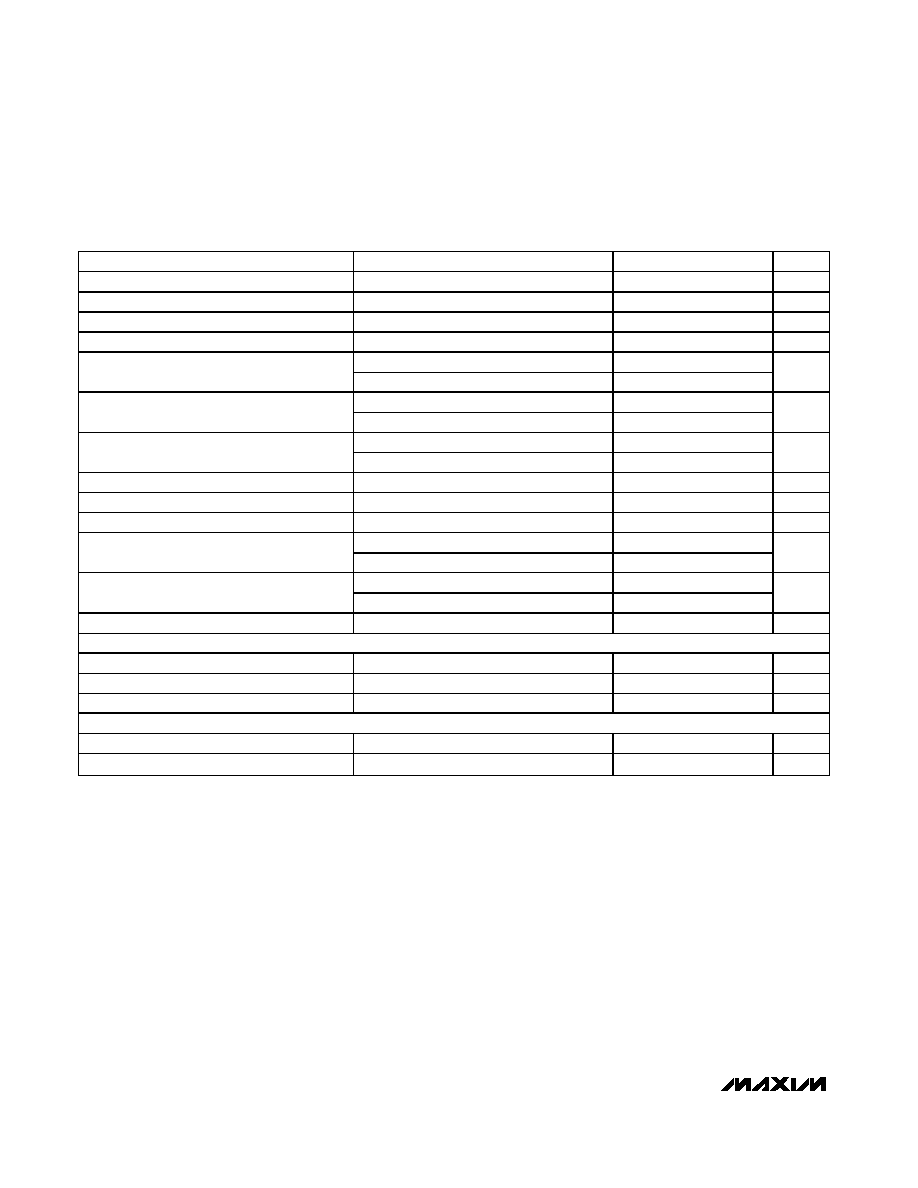
ELECTRICAL CHARACTERISTICS
(V
CC
= V
AVCC
= V
ONINV =
V
ONBST
= V
EN
= 3.6V, PGND = SEQ = GND, C6 = 0.22µF, C1 = 2.2µF, C2 = 6.7µF, Figure 1, T
A
= -40°C
to +85°C, unless otherwise noted.) (Note 3)
PARAMETER
CONDITIONS
MIN
TYP
MAX
UNITS
A
VCC
= V
CC
Voltage Range
(Note 1)
3
5.5
V
UVLO Threshold
V
CC
rising
2.42
2.82
V
Step-Up Output Voltage Adjust Range
V
AVCC
24
V
Inverter Output Voltage Adjust Range
V
INV
- V
CC
(Note 2)
-16
0
V
MAX8614B
0.7
0.9
LXP Current Limit
MAX8614A
0.34
0.52
A
MAX8614B
0.9
1.2
LXP Short-Circuit Current Limit
MAX8614A
0.52
0.70
A
MAX8614B
0.65
0.85
LXN Current Limit
MAX8614A
0.28
0.38
A
LXN On-Resistance
V
CC
= 3.6V
1.1
PVP On-Resistance
V
CC
= 3.6V
0.3
Maximum Duty Cycle
Step-up and inverter
82
%
I
AVCC
1.4
Quiescent Current (Switching, No Load)
I
VCC
3
mA
I
AVCC
800
Quiescent Current (No Switching, No Load)
I
VCC
15
µA
Oscillator Frequency
0.93
1.07
MHz
FBP, FBN, REFERENCE
REF Output Voltage
No load
1.235
1.260
V
FBP Threshold Voltage
No load
0.995
1.025
V
FBN Threshold Voltage
No load
-10
+10
mV
ONINV, ONBST SEQ LOGIC INPUTS
Logic-Low Input
2.7V < V
AVCC
< 5.5V
0.5
V
Logic-High Input
2.7V < V
AVCC
< 5.5V
1.6
V
Note 1: Output current and on-resistance are specified at 3.6V input voltage. The IC operates to 2.7V with reduced performance.
Note 2: The specified maximum negative output voltage is referred to V
CC
, and not to GND. With V
CC
= 3.3V, the maximum negative
output is then -12.7V.
Note 3: Specifications to -40°C are guaranteed by design, not production tested.
MAX8614A/MAX8614B
Dual-Output (+ and -) DC-DC
Converters for CCD
_______________________________________________________________________________________
5
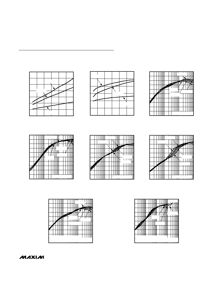
MAXIMUM OUTPUT CURRENT
vs. INPUT VOLTAGE
INPUT VOLTAGE (V)
MAXIMUM OUTPUT CURRENT (mA)
MAX8614A/B toc01
2.5
3.0
3.5
4.0
4.5
5.0
5.5
0
50
100
150
200
250
300
350
V
OUT
= 20V
V
OUT
= 15V
V
OUT
= 10V
MAXIMUM OUTPUT CURRENT
vs. INPUT VOLTAGE
INPUT VOLTAGE (V)
MAXIMUM OUTPUT CURRENT (mA) .
MAX8614A/B toc02
2.5
3.0
3.5
4.0
4.5
5.0
5.5
0
50
100
150
200
250
300
V
INV
= -10V
V
INV
= -7.5V
V
INV
= -5V
POSITIVE OUTPUT EFFICIENCY
vs. OUTPUT CURRENT
OUTPUT CURRENT (mA)
EFFICIENCY (%)
MAX8614A/B toc03
0.1
1
10
100
L = 2.2
µH, C = 2.2µF
0
10
20
30
40
50
60
70
80
90
100
V
CC
= 3V
V
CC
= 3.6V
V
CC
= 4.2V
V
CC
= 5V
POSITIVE OUTPUT EFFICIENCY
vs. OUTPUT CURRENT
OUTPUT CURRENT (mA)
EFFICIENCY (%)
MAX8614A/B toc04
0
10
20
30
40
50
60
70
80
90
100
0.1
1
10
100
L = 10
µH, C = 10µF
V
CC
= 3V
V
CC
= 3.6V
V
CC
= 4.2V
V
CC
= 5V
NEGATIVE OUTPUT EFFICIENCY
vs. OUTPUT CURRENT
OUTPUT CURRENT (mA)
EFFICIENCY (%)
MAX8614A/B toc05
0
10
20
30
40
50
60
70
80
90
100
0.1
1
10
100
L = 4.7
µH, C = 4.7µF
V
CC
= 3V
V
CC
= 3.6V
V
CC
= 4.2V
V
CC
= 5V
NEGATIVE OUTPUT EFFICIENCY
vs. OUTPUT CURRENT
OUTPUT CURRENT (mA)
EFFICIENCY (%)
MAX8614A/B toc06
0
10
20
30
40
50
60
70
80
90
100
0.1
1
10
100
L = 10
µH, C = 10µF
V
CC
= 3V
V
CC
= 3.6V
V
CC
= 4.2V
V
CC
= 5V
OUTPUT EFFICIENCY
vs. OUTPUT CURRENT
OUTPUT CURRENT (mA)
EFFICIENCY (%)
MAX8614A/B toc07
0
10
20
30
40
50
60
70
80
90
100
0.1
1
10
100
BOTH OUTPUTS LOADED EQUALLY
L1 = 2.2
µH, C1 = 2.2µF, L2 = 4.7µH, C2 = 4.7µF
V
CC
= 3V
V
CC
= 3.6V
V
CC
= 4.2V
V
CC
= 5V
OUTPUT EFFICIENCY
vs. OUTPUT CURRENT
OUTPUT CURRENT (mA)
EFFICIENCY (%)
MAX8614A/B toc08
0
10
20
30
40
50
60
70
80
90
100
0.1
1
10
100
1000
BOTH OUTPUTS LOADED EQUALLY
L1 = 10
µH, C1 = 10µF, L2 = 10µH, C2 = 10µF
V
CC
= 3V
V
CC
= 3.6V
V
CC
= 4.2V
V
CC
= 5V
Typical Operating Characteristics
(T
A
= +25°C, V
CC
= V
AVCC
= 3.6V, SEQ = GND, Figure 1, unless otherwise noted.)