General Description
The MAX8627 step-up converter is a high-efficiency,
low-quiescent current, synchronous boost converter
with True ShutdownTM and inrush current limiting. The
MAX8627 generates any boosted output voltage from
3V to 5V from either a 2-cell NiMH/NiCd or a single-cell
Li+/Li polymer battery.
Quiescent current is only 20µA (typ), and at light loads
the converter pulses only as needed for best efficiency.
At higher loads, PWM mode maintains fixed 1MHz
operation for lowest noise and ripple.
The MAX8627 includes an internal soft-start to limit
inrush current to a maximum of 500mA. Additional fea-
tures include True Shutdown, internal compensation,
and adjustable current limit. The MAX8627 is available
in a tiny 3mm x 3mm TDFN package and is ideal for
use in handheld devices such as DSCs, PDAs, and
smartphones.
Applications
DSC Motors and Backup Power
Microprocessor/DSP Core Power
Cellphones, PDAs, MP3 Players
Portable Handheld Devices
Features
1MHz PWM Switching Frequency
True Shutdown Output
Up to 95% Efficiency
1.0A Guaranteed Output Current
Soft-Start Eliminates Inrush Current
20µA (typ) Quiescent Current
0.1µA Logic-Controlled Shutdown
Internal Synchronous Rectifier
Internal Compensation
Adjustable Current Limit
Low-Noise Antiringing Feature
Tiny 14-Pin, 3mm x 3mm, TDFN Package
MAX8627
Low V
BATT
, 20µA IQ, 1MHz Synchronous
Boost Converter with True Shutdown
________________________________________________________________ Maxim Integrated Products
1
MAX8627ETD+
TDFN 3mm x 3mm
+
TOP VIEW
2
4
5
13
11
10
ILIM
PG
PG
FB
BATT
BATT
1
14
OUTS
GND
3
12
AGND
ON
6
9
LX
POUT
7
8
LX
POUT
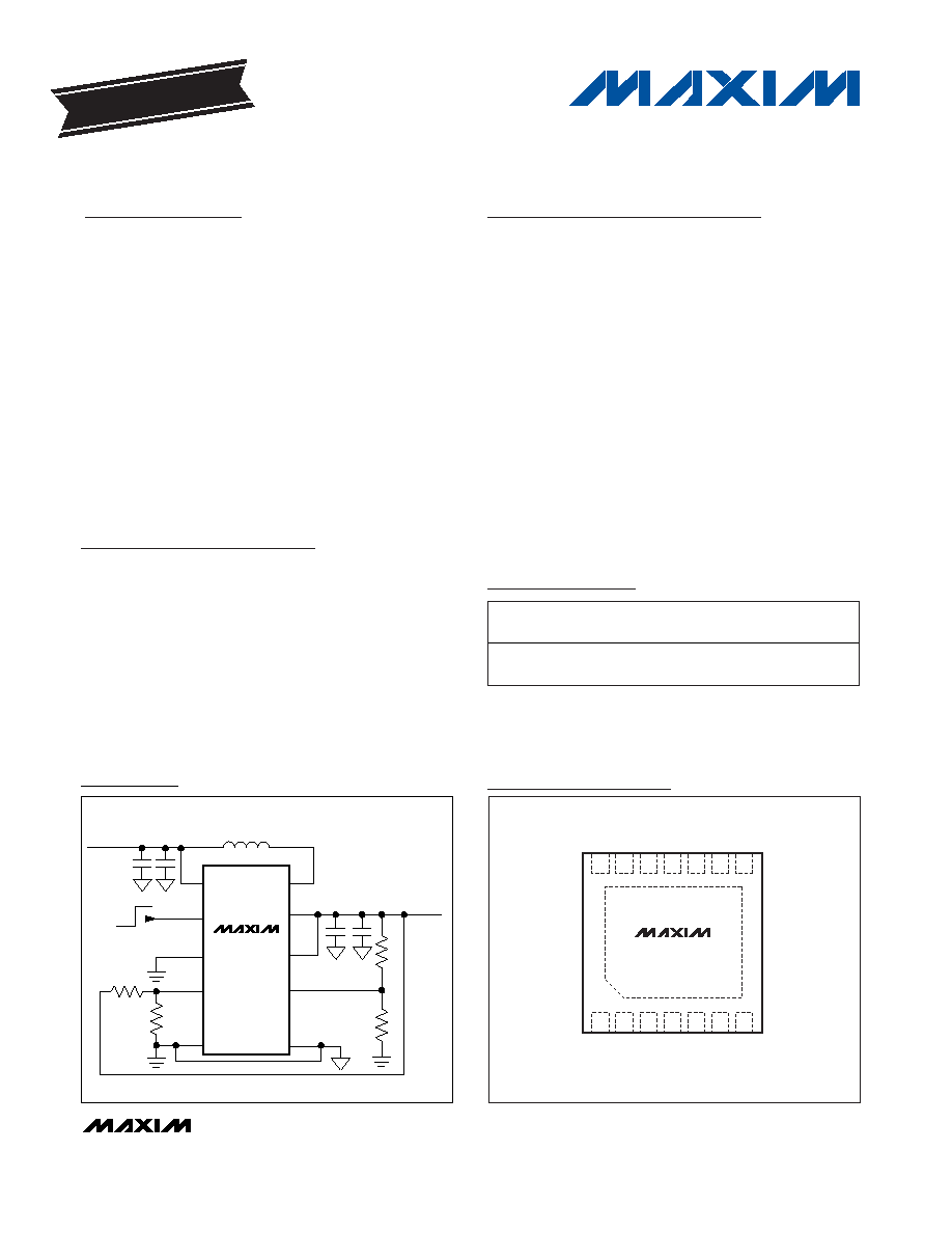
Pin Configuration
Ordering Information
19-3995; Rev 0; 3/06
For pricing, delivery, and ordering information, please contact Maxim/Dallas Direct! at
1-888-629-4642, or visit Maxim's website at www.maxim-ic.com.
Note: The device operates in the -40
∞C to +85∞C extended oper-
ating temperature range.
*EP = Exposed pad.
+Denotes lead-free package.
PART
PIN-
PACKAGE
PKG
CODE
TOP
MARK
MAX8627ETD+
14 TDFN-EP*
3mm x 3mm
T1433-2
AAQ
True Shutdown is a trademark of Maxim Integrated Products, Inc.
EVALUATION KIT
AVAILABLE
MAX8627
BATT
ON
ILIM
GND
LX
POUT
OUTS
FB
INPUT BATTERY
2.5V TO 4.2V
OUTPUT
3V TO 5V
UP TO 1A
ON
C2
C3
R1
R2
R3
R4
C4
L1
OFF
4, 5
3
AGND
12
1
13
2
PGND
10, 11
14
6,7
8, 9
C1
Typical Operating Circuit

MAX8627
Low V
BATT
, 20µA IQ, 1MHz Synchronous
Boost Converter with True Shutdown
2
_______________________________________________________________________________________
ABSOLUTE MAXIMUM RATINGS
ELECTRICAL CHARACTERISTICS
(V
OUTS
= V
POUT
= 5V, V
ON
= V
BATT
= 3.6V, V
ILIM
= GND, T
A
= -40∞C to +85∞C, typical values are at T
A
= +25
∞C, unless otherwise
noted.)
Stresses beyond those listed under "Absolute Maximum Ratings" may cause permanent damage to the device. These are stress ratings only, and functional
operation of the device at these or any other conditions beyond those indicated in the operational sections of the specifications is not implied. Exposure to
absolute maximum rating conditions for extended periods may affect device reliability.
OUTS, BATT to GND ................................................-0.3V to +6V
LX Current (Note 1) ...............................................................3.5A
AGND, PG to GND ................................................-0.3V to +0.3V
POUT to OUTS ......................................................-0.3V to +0.3V
FB, ILIM, ON to
GND.....0.3V to the higher of (V
OUTS
+ 0.3V) and (V
BATT
+ 0.3V)
Continuous Power Dissipation (T
A
= +70
∞C)
14-Pin TDFN 3mm x 3mm
(derate 18.2mW/
∞C above +70∞C).............................1454mW
Operating Temperature Range ...........................-40
∞C to +85∞C
Junction Temperature ......................................................+150
∞C
Storage Temperature Range .............................-65
∞C to +150∞C
Lead Temperature (soldering, 10s) .................................+300
∞C
PARAMETER
CONDITIONS
MIN
TYP
MAX
UNITS
GENERAL
Operating Input Voltage Range
(Note 1)
0.9
5.5
V
Minimum Startup Voltage
No load (Note 1)
1.2
1.5
V
Maximum Startup Current Limit
0.5
A
T
A
= +25
∞C
0.1
1
Shutdown, ON = GND
T
A
= +85
∞C
0.2
T
A
= 0
∞C to +85∞C
20
30
No load, no switching
T
A
= -40
∞C (Note 2)
20
35
Supply Current
No load, switching
20
µA
OSCILLATOR
Switching Frequency
0.95
1.0
1.05
MHz
Startup Switching Frequency
2.0
MHz
Maximum Duty Cycle
82.5
87.0
%
Output Voltage Adjust Range
3.0
5.2
V
FB Regulation Voltage
No load
1.005
1.015
1.025
V
FB Load Regulation
0A to 1A output current load step
-30
mV/A
FB Line Regulation
V
BATT
= 2.7V to 3V, output current = 0.5A
+20
mV
T
A
= +25
∞C
-50
-10
+50
FB Input Leakage Current
V
FB
= 1.2V,
V
OUTS
= V
POUT
= V
BATT
= 5.5V T
A
= +85
∞C
-10
nA
Low level
0.25
ILIM Dual ModeTM Threshold
High level
0.45
V
Idle Mode Trip Level
(Note 3)
50
mA
DC-DC SWITCHES
n-Channel On-Resistance
0.15
0.25
p-Channel On-Resistance
0.15
0.25
Damping Switch On-Resistance
17
30
V
ILIM
= 0V
3.2
3.5
3.7
n-Channel Current limit
V
ILIM
= 0.6V
1.0
A
Dual Mode is a trademark of Maxim Integrated Products, Inc.
Note 1: LX has internal clamp diodes to the IC internal power node V
PWR
(where V
PWR
is the higher of BATT or POUT) and PG.
Applications that forward bias these diodes should take care not to exceed the device's power-dissipation limits.
MAX8627
Low V
BATT
, 20µA IQ, 1MHz Synchronous
Boost Converter with True Shutdown
_______________________________________________________________________________________
3
ELECTRICAL CHARACTERISTICS (continued)
(V
OUTS
= V
POUT
= 5V, V
ON
= V
BATT
= 3.6V, V
ILIM
= GND, T
A
= -40∞C to +85∞C, typical values are at T
A
= +25
∞C, unless otherwise
noted.)
PARAMETER
CONDITIONS
MIN
TYP
MAX
UNITS
p-Channel Turn-Off Current
10
mA
T
A
= +25
∞C
0.1
1
POUT Leakage Current
V
LX
= 0V, V
POUT
= V
BATT
= 5.5V
T
A
= +85
∞C
0.2
µA
T
A
= +25
∞C
0.1
1
LX Leakage Current
V
LX
= 0V and V
POUT
= 5.5V or V
LX
=
5.5V and V
OUTS
= V
POUT
= 0V
T
A
= +85
∞C
0.2
µA
Soft-Start Interval
Output current = 0.5A
5.25
ms
Overload Protection Fault Delay
65
ms
LOGIC INPUTS
1.5V < V
POUT
= V
OUTS
= V
BATT
1.8V
0.2
ON Input Low Level
1.8V < V
POUT
= V
OUTS
= V
BATT
5.5V
0.5
V
1.5V < V
POUT
= V
OUTS
= V
BATT
1.8V
V
POUT
-
0.2
ON Input High Level
1.8V < V
POUT
= V
OUTS
+ V
BATT
5.5V
1.6
V
T
A
= +25
∞C
0.01
1
ON, Input Leakage Current
V
OUTS
= V
POUT
= V
BATT
= 5.5V,
ON = 0V or ON = 5.5V
T
A
= +85
∞C
0.02
µA
Thermal Shutdown
+160
∞C
Note 1: The MAX8627 is powered from OUTS. Once started, the IC operates down to 0.9V.
Note 2: Specifications to -40
∞C are guaranteed by design and not production tested.
Note 3: The idle-mode current threshold is the transition point between fixed-frequency PWM operation and idle-mode operation.
The specification is given in terms of output load current for an inductor value of 1µH. For a step-up converter, the idle-
mode transition varies with the input-to-output voltage ratio.
MAX8627
Low V
BATT
, 20µA IQ, 1MHz Synchronous
Boost Converter with True Shutdown
4
_______________________________________________________________________________________
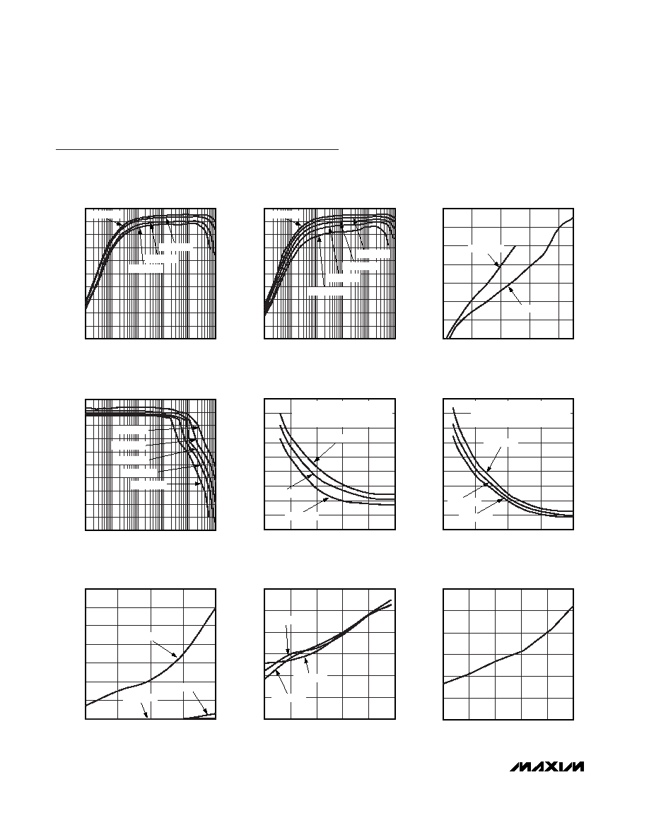
EFFICIENCY vs. LOAD CURRENT
WITH 3.3V OUTPUT
MAX8627 toc01
LOAD CURRENT (mA)
EFFICIENCY (%)
100
10
1
0.1
10
20
30
40
50
60
70
80
90
100
0
0.01
1000
V
BATT
= 3.0V
V
BATT
= 1.5V
V
BATT
= 1.8V
V
BATT
= 2.4V
EFFICIENCY vs. LOAD CURRENT
WITH 5V OUTPUT
MAX8627 toc02
LOAD CURRENT (mA)
EFFICIENCY (%)
100
10
1
0.1
10
20
30
40
50
60
70
80
90
100
0
0.01
1000
V
BATT
= 4.2V
V
BATT
= 1.8V
V
BATT
= 2.4V
V
BATT
= 3.0V
V
BATT
= 3.6V
MAXIMUM LOAD CURRENT
vs. INPUT VOLTAGE
MAX8627 toc03
INPUT VOLTAGE (V)
MAXIMUM LOAD CURRENT (A)
5.0
4.0
3.0
2.0
0.5
1.0
1.5
2.0
2.5
3.0
3.5
0
1.0
V
POUT
= 3.3V
V
POUT
= 5V
OUTPUT VOLTAGE vs. LOAD CURRENT
MAX8627 toc04
LOAD CURRENT (mA)
OUTPUT VOLTAGE (V)
100
10
1
0.1
4.94
4.96
4.98
5.00
5.02
5.04
5.06
5.08
5.10
5.12
4.92
0.01
1000
V
BATT
= 4.2V
V
BATT
= 1.8V
V
BATT
= 2.4V
V
BATT
= 3.0V
V
BATT
= 3.6V
NO-LOAD INPUT CURRENT
vs. INPUT VOLTAGE WITH 3.3V OUTPUT
MAX8627 toc05
INPUT VOLTAGE (V)
INPUT CURRENT (mA)
3.0
2.5
2.0
1.5
10
20
30
40
50
60
70
80
90
0
1.0
3.5
T
A
= +25
∞C
T
A
= +85
∞C
T
A
= 40
∞C
R1 = 1.15M
, R2 = 499k
OUTPUT ONLY LOADED WITH THE FB
RESISTOR-DIVIDER NETWORK.
NO-LOAD INPUT CURRENT
vs. INPUT VOLTAGE WITH 5V OUTPUT
MAX8627 toc06
INPUT VOLTAGE (V)
INPUT CURRENT (mA)
4
3
2
20
40
60
80
100
120
140
160
180
0
1
5
T
A
= +25
∞C
T
A
= +85
∞C
T
A
= 40
∞C
R1 = 2M
, R2 = 499k
OUTPUT ONLY LOADED WITH THE FB
RESISTOR-DIVIDER NETWORK.
SHUTDOWN CURRENT
vs. INPUT VOLTAGE
MAX8627 toc07
INPUT VOLTAGE (V)
SHUTDOWN CURRENT (nA)
4.5
3.5
2.5
100
200
300
400
500
600
700
0
1.5
5.5
T
A
= +25
∞C
T
A
= +85
∞C
T
A
= 40
∞C
STARTUP VOLTAGE vs. LOAD CURRENT
WITH 5V OUTPUT
MAX8627 toc08
LOAD CURRENT (mA)
STARTUP VOLTAGE (V)
600
800
400
200
0.5
1.0
1.5
2.0
2.5
3.0
0
0
1000
T
A
= +25
∞C
T
A
= +85
∞C
T
A
= 40
∞C
SOFT-START TIME vs. LOAD CURRENT
MAX8627 toc09
LOAD CURRENT (A)
SOFT-START TIME (ms)
0.3
0.4
0.2
0.1
1
2
3
4
5
6
0
0
0.5
Typical Operating Characteristics
(Circuit of
Figure
1, V
OUTS
= V
POUT
= 5V, V
ON
= V
BATT
= 3.6V, T
A
= +25
∞C, unless otherwise noted.)
MAX8627
Low V
BATT
, 20µA IQ, 1MHz Synchronous
Boost Converter with True Shutdown
_______________________________________________________________________________________
5
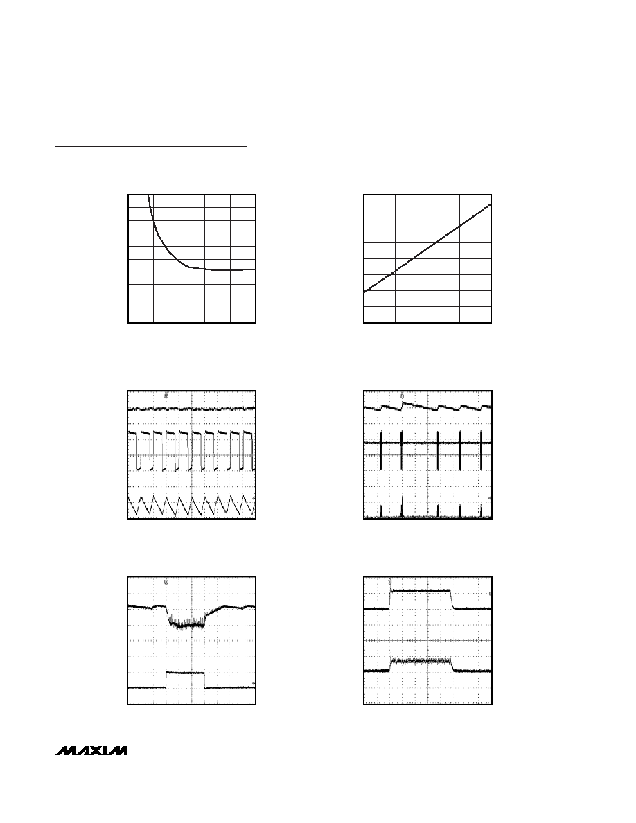
SOFT-START TIME vs. INPUT VOLTAGE
MAX8627 toc10
INPUT VOLTAGE (V)
SOFT-START TIME (ms)
3.5
4.5
2.5
1.5
2.5
3.0
3.5
0.5
1.5
1.0
2.0
4.0
4.5
5.0
0
0.5
5.5
PEAK INDUCTOR CURRENT vs. V
ILIM
MAX8627 toc11
V
ILIM
(V)
PEAK INDUCTOR CURRENT (A)
1.05
0.85
0.65
2.0
2.5
3.0
0.5
1.0
1.5
3.5
4.0
0
0.45
1.25
HEAVY LOAD SWITCHING WAVEFORMS
MAX8627 toc12
1
s/div
V
LX
I
LI
V
POUT
100mV/div
(AC-COUPLED)
2V/div
1A/div
0
0
LIGHT-LOAD SWITCHING WAVEFORMS
MAX8627 toc13
40
s/div
V
LX
I
LI
V
POUT
100mV/div
(AC-COUPLED)
2V/div
1A/div
0
0
LOAD TRANSIENT RESPONSE
MAX8627 toc14
20
s/div
I
LOAD
V
POUT
100mV/div
(AC-COUPLED)
500mA/div
0
LINE TRANSIENT RESPONSE
MAX8627 toc15
100
s/div
V
POUT
V
BATT
2V/div
100mV/div
(AC-COUPLED)
0
Typical Operating Characteristics (continued)
(Circuit of
Figure
1, V
OUTS
= V
POUT
= 5V, V
ON
= V
BATT
= 3.6V, T
A
= +25
∞C, unless otherwise noted.)