EVALUATION KIT
AVAILABLE
General Description
The MAX8631X/Y charge pump drives up to eight white
LEDs with regulated constant current for uniform inten-
sity. The main group of LEDs (M1≠M4) can be driven
up to 30mA per LED for backlighting. The flash group
of LEDs (F1≠F4) is independently controlled and can be
driven up to 100mA per LED (or 400mA total). Two
200mA LDOs are on-board to provide power for cam-
era functions. The LDOs' output voltages are pin-pro-
grammable to meet different camera-module
requirements. By utilizing adaptive 1x/1.5x/2x charge-
pump modes and very-low-dropout current regulators,
the MAX8631X/Y achieves high efficiency over the full
1-cell lithium-battery voltage range. The 1MHz fixed-fre-
quency switching allows for tiny external components,
and the regulation scheme is optimized to ensure low
EMI and low input ripple.
The MAX8631X/Y is available in a 28-pin thin QFN,
4mm x 4mm lead-free package (0.8mm max height).
Applications
Camera Phones and Smartphones
Backlighting and Flash
PDAs, Digital Cameras, and Camcorders
Features
Powers Up to 8 LEDs
Up to 30mA/LED Drive for Backlight
Up to 400mA Total Drive for Flash
Two Internal Low-Noise 200mA LDOs
94% Max/85% Avg Efficiency (P
LED
/P
BATT
) over Li+
Battery Discharge
0.2% Typical LED Current Matching
Adaptive 1x/1.5x/2x Mode Switchover
Flexible Brightness Control
Single-Wire Serial Pulse Interface (32 Steps)
2-Bit Logic (Three Levels)
Thermal T
A
Derating Function
Low Input Ripple and EMI
2.7V to 5.5V Supply Voltage Range
Soft-Start, Overvoltage, and Thermal-Shutdown
Protection
28-Pin Thin QFN, 4mm x 4mm Package
MAX8631X/Y
1x/1.5x/2x White LED Charge Pump with
Two LDOs in 4mm x 4mm Thin QFN
________________________________________________________________ Maxim Integrated Products
1
Ordering Information
19-3688; Rev 2; 5/06
For pricing, delivery, and ordering information, please contact Maxim/Dallas Direct! at
1-888-629-4642, or visit Maxim's website at www.maxim-ic.com.
PART
TEMP RANGE
PIN-PACKAGE
MAX8631XETI+
-40∞C to +85∞C
28 Thin QFN-EP*
4mm x 4mm (T2844-1)
MAX8631YETI+
-40∞C to +85∞C
28 Thin QFN-EP*
4mm x 4mm (T2844-1)
Pin Configuration appears at end of data sheet.
MAIN ON/OFF
AND DIMMING
MAX8631X/Y
1
µF
10
µF
0.01
µF
10
µF
PIN
IN
PGND
GND
P1
P2
OUT
MAIN
FLASH
OUTPUT
UP TO 480mA
1
µF
1
µF
LDO1
LDO2
C2P
C2N
1
µF
C1P
C1N
REF
SETM
SETF
CAMERA
MODULE
DUAL-LDO
VOLTAGE
SELECTION
INPUT
2.7V TO 5.5V
ENM2
ENM1
ENF
ENLDO
M1
M2
M3
M4
F1
F2
F3
F4
FLASH ON/OFF
DUAL-LDO ON/OFF
Typical Operating Circuit
*EP = Exposed paddle.
+Denotes lead-free package.
MAX8631X/Y
1x/1.5x/2x White LED Charge Pump with Two
LDOs in 4mm x 4mm Thin QFN
2
_______________________________________________________________________________________
ABSOLUTE MAXIMUM RATINGS
ELECTRICAL CHARACTERISTICS
(V
IN
= 3.6V, V
GND
= V
PGND
= 0V, ENM1 = ENM2 = ENF = IN, R
SETM
= R
SETF
= 6.8k
, P1 = P2 = unconnected, C
REF
= 0.01µF,
T
A
= -40∞C to +85∞C, unless otherwise noted. Typical values are at T
A
= +25∞C.) (Note 1)
Stresses beyond those listed under "Absolute Maximum Ratings" may cause permanent damage to the device. These are stress ratings only, and functional
operation of the device at these or any other conditions beyond those indicated in the operational sections of the specifications is not implied. Exposure to
absolute maximum rating conditions for extended periods may affect device reliability.
PIN, IN, OUT, REFBP to GND................................-0.3V to +6.0V
SETF, SETM, ENLDO, ENM1, ENM2, ENF,
P1, P2, LDO1, LDO2 to GND....................-0.3V to (V
IN
+ 0.3V)
M1, M2, M3, M4, F1, F2, F3, F4 to GND...-0.3V to (V
OUT
+ 0.3V)
C1N, C2N to GND ......................................... -0.3V to (V
IN
+ 1V)
C1P, C2P
to GND.............. -0.3V to greater of (V
OUT
+ 1V) or (V
IN
+ 1V)
PGND to GND .......................................................-0.3V to +0.3V
OUT, LDO1, LDO2 Short-Circuit to GND ...................Continuous
Continuous Power Dissipation (T
A
= +70∞C)
28-Pin Thin QFN 4mm X 4mm
(derate 20.8mW/∞C above +70∞C) .............................1666mW
Operating Temperature Range ...........................-40∞C to +85∞C
Junction Temperature ......................................................+150∞C
Storage Temperature Range .............................-65∞C to +150∞C
Lead Temperature (soldering, 10s) .................................+300∞C
PARAMETER
CONDITIONS
MIN
TYP
MAX
UNITS
IN Operating Voltage
2.7
5.5
V
Undervoltage-Lockout Threshold
V
IN
rising or falling
2.25
2.45
2.60
V
Undervoltage-Lockout Hysteresis
130
mV
1MHz switching, no load, 1.5x or 2x mode
4.0
5.5
1x mode 10% setting, ENF = GND, V
ENLDO
= V
IN
,
I
LDO1
= I
LDO2
= 0A
0.4
mA
Supply Current
ENM1 = ENM2 = ENF = GND, V
ENLDO
= V
IN
,
I
LDO1
= I
LDO2
= 0A
110
µA
T
A
= +25∞C
0.01
5
Shutdown Supply Current
ENM1 = ENM2 = ENF = ENLDO = GND
T
A
= +85∞C
0.1
µA
EN_ High Voltage
V
IN
= 2.7V to 5.5V
1.4
V
EN_ Low Voltage
V
IN
= 2.7V to 5.5V
0.4
V
T
A
= +25∞C
0.01
1
EN_ Input Current
V
EN_
= 0V or 5.5V
T
A
= +85∞C
0.1
µA
ENM_ or ENF Low Shutdown
Delay t
SHDN
See Figure 2
1.5
2
2.5
ms
ENM_ or ENF t
LO
See Figure 2
0.5
250.0
µs
ENM_ or ENF t
HI
See Figure 2
0.5
µs
Initial ENM_ or ENF t
HI
Only required for first ENM_ or ENF pulse, see Figure 2
200
µs
P1, P2 Shutdown Input Current
1
µA
P1, P2 Input Impedance
150
k
Thermal-Shutdown Threshold
Temperature rising
+160
∞C
Thermal-Shutdown Hysteresis
20
∞C
CHARGE PUMP
Overvoltage-Protection Threshold
V
OUT
rising
5
V
Soft-Start Time
2
ms
MAX8631X/Y
1x/1.5x/2x White LED Charge Pump with Two
LDOs in 4mm x 4mm Thin QFN
_______________________________________________________________________________________
3
ELECTRICAL CHARACTERISTICS (continued)
(V
IN
= 3.6V, V
GND
= V
PGND
= 0V, ENM1 = ENM2 = ENF = IN, R
SETM
= R
SETF
= 6.8k
, P1 = P2 = unconnected, C
REF
= 0.01µF,
T
A
= -40∞C to +85∞C, unless otherwise noted. Typical values are at T
A
= +25∞C.) (Note 1)
PARAMETER
CONDITIONS
MIN
TYP
MAX
UNITS
1x to 1.5x or 1.5x to 2x Mode
Transition Threshold
90
100
110
mV
Input Voltage-Mode Transition
Hysteresis
150
mV
Charge-Pump Maximum OUT
Current
V
IN
3.15V, V
OUT
= 3.9V
580
mA
1x mode, (V
IN
- V
OUT
) / I
OUT
0.3
1.0
1.5x mode, (1.5V
IN
- V
OUT
) / I
OUT
1.1
4.0
Open-Loop OUT Resistance
2x mode, (2V
IN
- V
OUT
) / I
OUT
1.5
4.14
Charge-Pump Short-Circuit
Current
V
OUT
< 1.25V
500
mA
Switching Frequency
1
MHz
OUT Pulldown Resistance in
Shutdown
ENM_ = ENF = GND
5
k
LED DRIVER
SET_ Bias Voltage
T
A
= +25∞C
0.6
V
T
A
= +25∞C
0.01
1
SET_ Leakage in Shutdown
ENM_ = ENF = GND
T
A
= +85∞C
0.1
µA
SET_ Current Range
10
145
µA
SETM-to-Main LED Current Ratio
(I
M_
/I
SETM
)
100% setting, M1≠M4
230
A/A
SETF-to-Flash LED Current Ratio
(I
F_
/I
SETF
)
100% setting, F1≠F4
690
A/A
T
A
= +25∞C
-1.25
+1.25
M_, F_ Current Accuracy
T
A
= -40∞C to current derating start temperature
-4
+4
%
Maximum Main LED Sink Current
R
SETM
= 4.6k
, for each M_
30
mA
Maximum Flash LED Sink Current
R
SETF
= 4.12k
, I
F1
+ I
F2
+ I
F3
+ I
F4
400
mA
Current-Derating-Function Start
Temperature
+40
∞C
Current-Derating-Function Slope
T
A
= +40∞C to +85∞C
-1.7
%/∞C
Dropout Voltage
(Note 2)
40
90
mV
1.5x and 2x Regulation Voltage
150
mV
T
A
= +25∞C
0.01
1
M_, F_ Leakage in Shutdown
ENM_ = ENF = GND
T
A
= +85∞C
0.1
µA
LDO_
Output Voltage Accuracy
I
LDO_
= 150mA, relative to V
OUT(NOM)
(Note 3)
-1.7
0
+1.7
%
Output Current Range
0
200
mA
Current Limit
V
LDO_
= 0V
280
475
750
mA
Soft-Start Current Limit
160
mA
MAX8631X/Y
1x/1.5x/2x White LED Charge Pump with
Two LDOs in 4mm x 4mm Thin QFN
4
_______________________________________________________________________________________
ELECTRICAL CHARACTERISTICS (continued)
(V
IN
= 3.6V, V
GND
= V
PGND
= 0V, ENM1 = ENM2 = ENF = IN, R
SETM
= R
SETF
= 6.8k
, P1 = P2 = unconnected, C
REF
= 0.01µF,
T
A
= -40∞C to +85∞C, unless otherwise noted. Typical values are at T
A
= +25∞C.) (Note 1)
PARAMETER
CONDITIONS
MIN
TYP
MAX
UNITS
Soft-Start Done Time
100
µs
Dropout Voltage
I
LDO_
= 200mA (Note 4)
120
320
mV
Load Regulation
V
IN
= 3.7V, 100µA < I
LDO_
< 200mA
1.3
%
Power-Supply Rejection
V
OUT
/
V
IN
10Hz to 10kHz, C
LDO_
= 1µF, I
LDO_
= 10µA
-60
dB
Output Noise Voltage (RMS)
10Hz to 100kHz, C
LDO_
= 1µF, I
LDO_
= 10mA
40
µV
RMS
Note 1: All devices are 100% production tested at T
A
= +25∞C. Limits over the operating temperature range are guaranteed by
design.
Note 2: LED dropout voltage is defined as the M_ or F_ to GND voltage at which current into M_ or F_ drops 10% from the value at
M_ or F_ = 0.2V.
Note 3: (Greater of 2.7V or (V
LDO_
+ 0.5V))
V
IN
5.5V.
Note 4: LDO dropout voltage is defined as V
IN
- V
OUT
when V
OUT
is 100mV below the value of V
OUT
measured when V
IN
=
V
OUT(NOM)
+ 1V. Since the minimum input voltage is 2.7V, this specification is only meaningful when V
OUT(NOM)
> 2.5V.
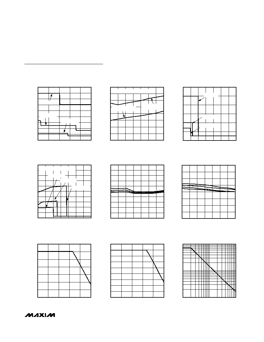
Typical Operating Characteristics
(V
IN
= V
EN_
= 3.6V, circuit of Figure 1, T
A
= +25∞C, unless otherwise noted.)
EFFICIENCY vs. Li+ BATTERY
VOLTAGE DRIVING FOUR MAIN LEDs
MAX8631X toc01
Li+ BATTERY VOLTAGE (V)
EFFICIENCY P
LED
/P
BATT
(%)
3.9
3.6
3.3
3.0
50
60
70
80
90
100
40
2.7
4.2
15mA/LED
4.5mA/LED
1.5mA/LED
EFFICIENCY vs. Li+ BATTERY
VOLTAGE DRIVING FLASH LED MODULE
MAX8631 toc02
Li+ BATTERY VOLTAGE (V)
EFFICIENCY P
LED
/P
BATT
(%)
3.9
3.6
3.3
3.0
50
60
70
80
90
100
40
2.7
4.2
80mA TOTAL
160mA TOTAL
400mA TOTAL
BATTERY CURRENT vs. SUPPLY VOLTAGE
DRIVING FOUR MAIN LEDs
MAX8631X toc03
SUPPLY VOLTAGE (V)
BATTERY CURRENT (mA)
3.9
3.6
3.3
3.0
20
40
60
80
100
120
0
2.7
4.2
I
LED
= 15mA
I
LED
= 4.5mA
I
LED
= 1.5mA
V
IN
FALLING
V
IN
RISING
MAX8631X/Y
1x/1.5x/2x White LED Charge Pump with
Two LDOs in 4mm x 4mm Thin QFN
_______________________________________________________________________________________
5
BATTERY CURRENT vs. SUPPLY
VOLTAGE DRIVING FLASH
MAX8631X toc04
SUPPLY VOLTAGE (V)
BATTERY CURRENT (mA)
3.9
3.6
3.3
3.0
100
200
300
400
500
600
700
800
900
0
2.7
4.2
I
FLASH
= 400mA
I
FLASH
= 160mA
I
FLASH
= 80mA
LDO GROUND PIN SUPPLY
CURRENT vs. SUPPLY VOLTAGE
MAX8631X toc05
SUPPLY VOLTAGE (V)
GROUND PIN SUPPLY CURRENT (
µ
A)
5.1
4.7
3.9
4.3
3.5
3.1
90
100
110
120
130
140
150
160
80
2.7
5.5
V
ENM
= V
ENF
= 0V, V
ENLDO
= V
IN
150mA, BOTH LDOs
NO LOAD, BOTH LDOs
INPUT RIPPLE VOLTAGE vs. SUPPLY
VOLTAGE WITH FOUR MAIN LEDs
MAX8631X toc06
SUPPLY VOLTAGE (V)
INPUT RIPPLE (mV
RMS
)
5.1
4.7
4.3
3.9
3.5
3.1
0.2
0.4
0.6
0.8
1.0
1.2
0
2.7
5.5
I
LED
= 15mA
I
LED
= 4.5mA
I
LED
= 1.5mA
INPUT RIPPLE VOLTAGE vs. SUPPLY
VOLTAGE WITH FLASH AND MAIN LEDs
MAX8631X toc07
SUPPLY VOLTAGE (V)
INPUT RIPPLE (mV
RMS
)
5.1
4.7
3.1
3.5
3.9
4.3
1
2
3
4
5
7
9
6
8
10
0
2.7
5.5
FOUR MAIN LEDs AT 15mA EACH
I
FLASH
= 10mA
I
FLASH
= 40mA
I
FLASH
= 100mA
LED CURRENT MATCHING vs. SUPPLY
VOLTAGE WITH FOUR MAIN LEDs
MAX8631X toc08
SUPPLY VOLTAGE (V)
MAIN LED CURRENT (mA)
5.1
4.7
3.9
4.3
3.5
3.1
14.2
14.4
14.6
14.8
15.0
15.2
15.4
15.6
15.8
16.0
14.0
2.7
5.5
LED CURRENT MATCHING vs. SUPPLY
VOLTAGE WITH FOUR FLASH LEDs
MAX8631X toc09
SUPPLY VOLTAGE (V)
FLASH LED CURRENT (mA)
5.1
4.7
4.3
3.9
3.5
3.1
99.0
98.5
99.5
100.0
100.5
101.0
101.5
102.0
98.0
2.7
5.5
LED CURRENT vs. AMBIENT
TEMPERATURE WITH FOUR MAIN LEDs
MAX8631X toc10
AMBIENT TEMPERATURE (
∞C)
TOTAL LED CURRENT (mA)
60
35
10
-15
10
20
30
40
50
60
70
0
-40
85
LED CURRENT vs. AMBIENT
TEMPERATURE WITH FLASH
MAX8631X toc11
AMBIENT TEMPERATURE (
∞C)
TOTAL LED CURRENT (mA)
60
35
10
-15
50
100
150
200
250
300
350
400
450
0
-40
85
INDIVIDUAL MAIN LED CURRENT
vs. R
SETM
MAX8631X toc12
R
SETM
(k
)
MAIN LED CURRENT (mA)
10
10
100
1
100
1
Typical Operating Characteristics (continued)
(V
IN
= V
EN_
= 3.6V, circuit of Figure 1, T
A
= +25∞C, unless otherwise noted.)