 | –≠–ª–µ–∫—Ç—Ä–æ–Ω–Ω—ã–π –∫–æ–º–ø–æ–Ω–µ–Ω—Ç: MAX870EUK | –°–∫–∞—á–∞—Ç—å:  PDF PDF  ZIP ZIP |
_______________General Description
The ultra-small MAX870/MAX871 monolithic, CMOS
charge-pump inverters accept input voltages ranging
from +1.4V to +5.5V. The MAX870 operates at 125kHz,
and the MAX871 operates at 500kHz. Their high efficien-
cy (90%) and low operating current (0.7mA for the
MAX870) make these devices ideal for both battery-pow-
ered and board-level voltage-conversion applications.
Oscillator control circuitry and four power MOSFET
switches are included on-chip. A typical MAX870/
MAX871 application is generating a -5V supply from a
+5V logic supply to power analog circuitry. Both parts
come in a 5-pin SOT23-5 package and can deliver 25mA
with a voltage drop of 500mV.
For applications requiring more power, the MAX860
delivers up to 50mA with a voltage drop of 600mV, in a
space-saving µMAX package.
________________________Applications
Local -5V Supply from 5V Logic Supply
Small LCD Panels
Cell Phones
Medical Instruments
Handy-Terminals, PDAs
Battery-Operated Equipment
____________________________Features
o
5-Pin SOT23-5 Package
o
99% Voltage Conversion Efficiency
o
Invert Input Supply Voltage
o
0.7mA Quiescent Current (MAX870)
o
+1.4V to +5.5V Input Voltage Range
o
Require Only Two Capacitors
o
25mA Output Current
o
Shutdown Control
MAX870/MAX871
Switched-Capacitor Voltage Inverters
________________________________________________________________
Maxim Integrated Products
1
TOP VIEW
IN
GND
C1-
C1+
OUT
SOT23-5
1
5
MAX870
MAX871
2
3
4
__________________Pin Configuration
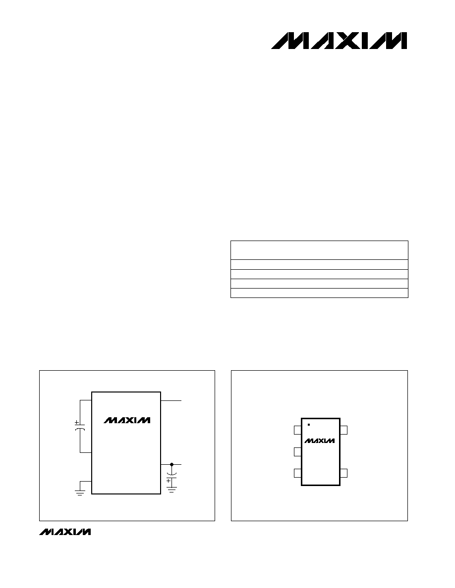
NEGATIVE VOLTAGE CONVERTER
C1+
C1-
IN
OUT
GND
INPUT
SUPPLY
VOLTAGE
NEGATIVE
OUTPUT
VOLTAGE
MAX870
MAX871
4
3
5
2
1
__________Typical Operating Circuit
19-1240; Rev 0; 6/97
PART
MAX870
C/D
MAX870EUK
-40∞C to +85∞C
0∞C to +70∞C
TEMP. RANGE
PIN-
PACKAGE
Dice*
5 SOT23-5
______________Ordering Information
*
Dice are tested at T
A
= +25∞C.
For free samples & the latest literature: http://www.maxim-ic.com, or phone 1-800-998-8800
MAX871
C/D
MAX871EUK
-40∞C to +85∞C
0∞C to +70∞C
Dice*
5 SOT23-5
SOT
TOP MARK
--
ABZN
--
ABZO
MAX870/MAX871
Switched-Capacitor Voltage Inverters
2
_______________________________________________________________________________________
ABSOLUTE MAXIMUM RATINGS
ELECTRICAL CHARACTERISTICS
(V
IN
= +5V, C1 = C2 = 1µF (MAX870), C1 = C2 = 0.33µF (MAX871),
T
A
= 0∞C to +85∞C
, unless otherwise noted. Typical values
are at T
A
= +25∞C.)
ELECTRICAL CHARACTERISTICS
(V
IN
= +5V, C1 = C2 = 1µF (MAX870), C1 = C2 = 0.33µF (MAX871),
T
A
= -40∞C to +85∞C
, unless otherwise noted.) (Note 2)
Stresses beyond those listed under "Absolute Maximum Ratings" may cause permanent damage to the device. These are stress ratings only, and functional
operation of the device at these or any other conditions beyond those indicated in the operational sections of the specifications is not implied. Exposure to
absolute maximum rating conditions for extended periods may affect device reliability.
Note 1:
Capacitor contribution is approximately 20% of the output impedance [ESR + 1 / (pump frequency x capacitance)].
Note 2:
All -40∞C to +85∞C specifications are guaranteed by design.
IN to GND ..............................................................+6.0V to -0.3V
OUT to GND ..........................................................-6.0V to +0.3V
C1+ ..............................................................(V
IN
+ 0.3V) to -0.3V
C1-............................................................(V
OUT
- 0.3V) to +0.3V
OUT Output Current ...........................................................50mA
OUT Short Circuit to GND .............................................Indefinite
Continuous Power Dissipation (T
A
= +70∞C)
SOT23-5 (derate 7.1mW/∞C above +70∞C)...................571mW
Operating Temperature Range
MAX870EUK/MAX871EUK ...............................-40∞C to +85∞C
Storage Temperature Range .............................-65∞C to +160∞C
Lead Temperature (soldering, 10sec) .............................+300∞C
MAX871
MAX870
R
LOAD
= 500k
,
T
A
=+25∞C
R
LOAD
= 10k
R
LOAD
= 10k
T
A
= +25∞C
CONDITIONS
mA
2.7
3.8
0.7
1.0
Supply Current
96
99
%
90
Power Efficiency
kHz
325
500
675
1.4
1.0
V
1.5
Minimum Supply Voltage
V
5.5
Maximum Supply Voltage
81
125
169
UNITS
MIN
TYP
MAX
PARAMETER
T
A
= +25∞C
T
A
= 0∞C to + 85∞C
25
MAX871
MAX870
I
OUT
= 5mA
MAX871
R
LOAD
= 10k
MAX870
CONDITIONS
mA
4.4
1.3
Supply Current
65
Output Resistance
kHz
225
775
Oscillator Frequency
V
1.6
Minimum Supply-Voltage Range
56
194
UNITS
MIN
TYP
MAX
PARAMETER
T
A
= +25∞C
Oscillator Frequency
C1 = C2 = 0.47µF
I
OUT
=
5mA
C1 = C2 = 1µF
Output Resistance (Note 1)
20
50
MAX870
T
A
= +25∞C
C1 = C2 = 0.33µF
20
50
C1 = C2 = 0.22µF
25
MAX871
C1 = C2 = 0.1µF
35
65
T
A
= 0∞C to + 85∞C
75
MAX870
MAX871
MAX870
MAX871
R
LOAD
=
,
T
A
=+25∞C
%
98
99.3
Voltage Conversion Efficiency
MAX870
MAX871
R
LOAD
=
%
97
Voltage Conversion Efficiency
95
MAX870
MAX871
R
LOAD
= 10k
V
5.5
Maximum Supply-Voltage Range

MAX870/MAX871
Switched-Capacitor Voltage Inverters
_______________________________________________________________________________________
3
0
0.5
1.0
1.5
2.0
2.5
3.0
1.5
2.5
2.0
3.0
3.5
4.0
4.5
5.0
5.5
SUPPLY CURRENT
vs. SUPPLY VOLTAGE
MAX870/71-TOC01
SUPPLY VOLTAGE (V)
SUPPLY CURRENT (mA)
MAX870
MAX871
60
10
1.5
2.5
3.0
2.0
OUTPUT RESISTANCE
vs. SUPPLY VOLTAGE
50
MAX828/829-02
SUPPLY VOLTAGE (V)
OUTPUT RESISTANCE (
)
3.5
4.0
5.5
4.5
5.0
40
20
30
MAX870
MAX871
0
15
10
5
20
25
30
35
40
45
50
-40
10
-15
35
60
85
MAX870
OUTPUT RESISTANCE vs. TEMPERATURE
MAX870/71 ROC3
TEMPERATURE (∞C)
OUTPUT RESISTANCE (
)
V
IN
= 1.5V
V
IN
= 3.3V
V
IN
= 5.0V
45
0
0
0.5
3.0
2.5
MAX870
OUTPUT CURRENT vs. CAPACITANCE
35
40
MAX870/871-04
CAPACITANCE (
µ
F)
OUTPUT CURRENT (mA)
1.0
1.5
2.0
3.5
30
25
20
10
5
15
V
IN
= 3.15V, V
OUT
= -2.5V
V
IN
= 1.9V, V
OUT
= -1.5V
V
IN
= 4.75V, V
OUT
= -4.0V
35
0
0
0.5
2.0
MAX871
OUTPUT CURRENT vs. CAPACITANCE
25
30
MAX870/871-07
CAPACITANCE (
µ
F)
OUTPUT CURRENT (mA)
1.0
1.5
2.5
20
15
10
5
V
IN
= 3.15V, V
OUT
= -2.5V
V
IN
= 1.9V, V
OUT
= -1.5V
V
IN
= 4.75V, V
OUT
= -4.0V
450
0
0
0.5
2.0 2.5 3.0
4.0
3.5
4.5
MAX870
OUTPUT VOLTAGE RIPPLE
vs. CAPACITANCE
50
350
400
MAX870/871-05
CAPACITANCE (
µ
F)
OUTPUT VOLTAGE RIPPLE (mVp-p)
1.5
1.0
5.0
300
250
200
150
100
V
IN
= 4.75V, V
OUT
= -4.0V
V
IN
= 3.15V, V
OUT
= -2.5V
V
IN
= 1.9V, V
OUT
= -1.5V
0
20
10
40
30
60
50
70
-40
10
-15
35
60
85
MAX871
OUTPUT RESISTANCE vs. TEMPERATURE
MAX870/71-TOC06
TEMPERATURE (∞C)
OUTPUT RESISTANCE (
)
V
IN
= 1.5V
V
IN
= 3.3V
V
IN
= 5.0V
0
150
100
50
200
250
300
350
400
450
500
0
1.0
0.5
1.5
2.0
2.5
MAX871
OUTPUT VOLTAGE RIPPLE
vs. CAPACITANCE
MAX870/71 TOC08
CAPACITANCE (
µ
F)
OUTPUT VOLTAGE RIPPLE (mVp-p)
V
IN
= 4.75V, V
OUT
= -4.0V
V
IN
= 3.15V, V
OUT
= -2.5V
V
IN
= 1.9V, V
OUT
= -1.5V
__________________________________________Typical Operating Characteristics
(Circuit of Figure 1, V
IN
= +5V, C1 = C2 = C3, T
A
= +25∞C, unless otherwise noted.)
-5.0
-4.0
-4.5
-3.0
-3.5
-2.0
-2.5
-1.5
-0.5
-1.0
0
0
10
15
20
5
25
30
35
40
45
MAX870
OUTPUT VOLTAGE
vs. OUTPUT CURRENT
MAX870/871-TOC9
OUTPUT CURRENT (mA)
OUTPUT VOLTAGE (V)
V
IN
= 2.0V
V
IN
= 3.3V
V
IN
= 5.0V
_____________________Pin Description
MAX870/MAX871
Switched-Capacitor Voltage Inverters
4
_______________________________________________________________________________________
____________________________Typical Operating Characteristics (continued)
(Circuit of Figure 1, V
IN
= +5V, C1 = C2 = C3, T
A
= +25∞C, unless otherwise noted.)
0
20
10
40
30
60
50
70
90
80
100
0
10 15 20
5
25 30 35
45
40
50
MAX870
EFFICIENCY vs. OUTPUT CURRENT
MAX870/71-TOC10
OUTPUT CURRENT (mA)
EFFICIENCY (%)
V
IN
= 2.0V
V
IN
= 3.3V
V
IN
= 5.0V
0
20
10
50
40
30
80
70
60
90
0
15
20
5
10
25
30
35
40
MAX871
EFFICIENCY vs. OUTPUT CURRENT
MAX870/71 TOC11
OUTPUT CURRENT (mA)
EFFICIENCY (%)
V
IN
= 2.0V
V
IN
= 3.3V
V
IN
= 5.0V
100
250
200
150
300
350
400
450
500
550
600
-40
10
-15
35
60
85
PUMP FREQUENCY vs. TEMPERATURE
MAX870/71-TOC12
TEMPERATURE (∞C)
PUMP FREQUENCY (kHz)
V
IN
= 1.5V, MAX871
V
IN
= 1.5V, MAX870
V
IN
= 3.3V OR 5.0V, MAX870
V
IN
= 3.3V OR 5.0V, MAX871
MAX870
OUTPUT NOISE AND RIPPLE
MAX870/71-TCC13
2
µ
s/div
V
IN
= 3.3V, V
OUT
= -3.18V, I
OUT
= 5mA,
20mV/div, AC COUPLED
Flying Capacitor's Positive Terminal
C1+
5
Ground
GND
4
Flying Capacitor's Negative Terminal
C1-
3
PIN
Positive Power-Supply Input
IN
2
Inverting Charge-Pump Output
OUT
1
FUNCTION
NAME
VOLTAGE INVERTER
OUT
IN
C1+
V
IN
R
L
C1
0.33
µ
F*
*1
µ
F
(MAX870)
C2
0.33
µ
F*
C3
0.33
µ
F*
5
1
2
3
4
V
OUT
GND
C1-
MAX870
MAX871
Figure 1. Test Circuit
MAX871
OUTPUT NOISE AND RIPPLE
MAX870/71-TCC14
1
µ
s/div
V
IN
= 3.3V, V
OUT
= -3.14V, I
OUT
= 5mA,
20mV/div, AC COUPLED
_______________Detailed Description
The MAX870/MAX871 capacitive charge pumps invert
the voltage applied to their input. For highest perfor-
mance, use low equivalent series resistance (ESR)
capacitors (e.g., ceramic).
During the first half-cycle, switches S2 and S4 open,
switches S1 and S3 close, and capacitor C1 charges to
the voltage at IN (Figure 2). During the second half-
cycle, S1 and S3 open, S2 and S4 close, and C1 is level
shifted downward by V
IN
volts. This connects C1 in par-
allel with the reservoir capacitor C2. If the voltage across
C2 is smaller than the voltage across C1, then charge
flows from C1 to C2 until the voltage across C2 reaches
-V
IN
. The actual voltage at the output is more positive
than -V
IN
, since switches S1≠S4 have resistance and the
load drains charge from C2.
Charge-Pump Output
The MAX870/MAX871 are not voltage regulators: the
charge pump's output source resistance is approxi-
mately 20
at room temperature (with V
IN
= +5V), and
V
OUT
approaches -5V when lightly loaded. V
OUT
will
droop toward GND as load current increases. The
droop of the negative supply (V
DROOP-
) equals the cur-
rent draw from OUT (I
OUT
) times the negative convert-
er's source resistance (RS-):
V
DROOP-
= I
OUT
x RS-
The negative output voltage will be:
V
OUT
= -(V
IN
≠ V
DROOP-
)
Efficiency Considerations
The power efficiency of a switched-capacitor voltage
converter is affected by three factors: the internal loss-
es in the converter IC, the resistive losses of the pump
capacitors, and the conversion losses during charge
transfer between the capacitors. The total power loss is:
The internal losses are associated with the IC's internal
functions, such as driving the switches, oscillator, etc.
These losses are affected by operating conditions such
as input voltage, temperature, and frequency.
The next two losses are associated with the voltage
converter circuit's output resistance. Switch losses
occur because of the on-resistance of the MOSFET
switches in the IC. Charge-pump capacitor losses
occur because of their ESR. The relationship between
these losses and the output resistance is as follows:
where f
OSC
is the oscillator frequency. The first term is
the effective resistance from an ideal switched-
capacitor circuit. See Figures 3a and 3b.
P
= P
+ P
+ P
+ P
LOSS
INTERNAL LOSSES
SWITCH LOSSES
PUMP CAPACITOR LOSSES
CONVERSION LOSSES
MAX870/MAX871
Switched-Capacitor Voltage Inverters
_______________________________________________________________________________________
5
S1
IN
S2
S3
S4
C1
C2
V
OUT
= -(V
IN
)
Figure 2. Ideal Voltage Inverter
V+
C1
f
C2
R
L
V
OUT
Figure 3a. Switched-Capacitor Model
R
EQUIV
=
R
EQUIV
V
OUT
R
L
1
V+
f
◊
C1
C2
Figure 3b. Equivalent Circuit
P
+P
= I
x R
PUMP CAPACITOR LOSSES
CONVERSION LOSSES
OUT
2
OUT
R
f
x C
R
ESR
ESR
OUT
OSC
SWITCHES
C
C
( )
+
+
+
1
1
2
4
1
2