
For free samples & the latest literature: http://www.maxim-ic.com, or phone 1-800-998-8800.
For small orders, phone 1-800-835-8769.
General Description
The MAX8860 low-noise, low-dropout linear regulator
operates from a +2.5V to +6.5V input and is guaran-
teed to deliver 300mA. Typical output noise for this
device is 60µV
RMS
, and typical dropout is 105mV at
200mA. In addition to the six available preset output
voltages (+1.8V, +2.5V, +2.77V, +2.82V, +3.0V, and
+3.3V), the Dual ModeTM feature allows the device to
be configured as an adjustable output regulator from
+1.25V to +6.5V.
Designed with an internal P-channel MOSFET pass tran-
sistor, the MAX8860 has a low 120µA supply current. An
output fault-detection circuit indicates loss of regulation.
Other features include a 10nA, logic-controlled shut-
down mode, short-circuit and thermal-shutdown protec-
tion, and reverse battery protection. The MAX8860 is
available in a miniature 8-pin µMAX package.
Applications
Wireless Handsets
DSP Core Power
PCMCIA Cards
Hand-Held Instruments
Palmtop Computers
Electronic Planners
Features
o High Output Current (300mA)
o Low Output Voltage Noise: 60µV
RMS
o Low 105mV Dropout at 200mA Output
o Low 120µA No-Load Supply Current
o Thermal-Overload and Short-Circuit Protection
o Reverse Battery Protection
o 10nA Logic-Controlled Shutdown
o FAULT Indicator
o Small, Space-Saving µMAX Package
(1.1mm max height)
o Small 2.2µF Output Capacitor
Saves Space and Cost
MAX8860
Low-Dropout, 300mA
Linear Regulator in µMAX
________________________________________________________________ Maxim Integrated Products
1
1
2
3
4
8
7
6
5
FAULT
SHDN
CC
SET
OUT
GND
IN
OUT
MAX8860
µMAX
TOP VIEW
MAX8860
OUT
OUT
CC
SET
FAULT
GND
IN
SHDN
C1
2.2µF
C2
2.2µF
C3
33nF
OUTPUT
UP TO
300mA
INPUT
+2.5V TO
+6.5V
FAULT-
DETECT
OUTPUT
R1
100k
Typical Operating Circuit
19-1422; Rev 1; 12/99
MAX8860EUA18
MAX8860EUA28
-40∞C to +85∞C
-40∞C to +85∞C
8 µMAX
8 µMAX
Pin Configuration
Ordering Information
Dual Mode is a trademark of Maxim Integrated Products.
MAX8860EUA33
-40∞C to +85∞C
8 µMAX
PART
TEMP. RANGE
PIN-
PACKAGE
+1.80
+2.82
+3.30
V
OUT
(V)
+2.77
MAX8860EUA27
-40∞C to +85∞C
8 µMAX
+2.50
MAX8860EUA25
-40∞C to +85∞C
8 µMAX
MAX8860EUA30
-40∞C to +85∞C
+3.00
8 µMAX

MAX8860
Low-Dropout, 300mA
Linear Regulator in µMAX
2
_______________________________________________________________________________________
ABSOLUTE MAXIMUM RATINGS
ELECTRICAL CHARACTERISTICS
(V
IN
= +3.6V, C
CC
= 33nF, T
A
= -40∞C to +85∞C, unless otherwise noted. Typical values are at T
A
= +25∞C.) (Note 1)
Stresses beyond those listed under "Absolute Maximum Ratings" may cause permanent damage to the device. These are stress ratings only, and functional
operation of the device at these or any other conditions beyond those indicated in the operational sections of the specifications is not implied. Exposure to
absolute maximum rating conditions for extended periods may affect device reliability.
IN, SHDN to GND .......................................................-7V to +7V
SHDN to IN ...............................................................-7V to +0.3V
SET, CC, FAULT to GND ..........................................-0.3V to +7V
OUT to GND .............................................. -0.3V to (V
IN
+ 0.3V)
FAULT Sink Current ...........................................................20mA
Continuous Output Current ..............................................330mA
Output Short-Circuit Duration ....................................Continuous
Continuous Power Dissipation (T
A
= +70∞C)
8-Pin µMAX (derate 4.1mW/∞C above +70∞C) ............330mW
Thermal Resistance (
JA
)
8-Pin µMAX ............................................................+244∞C/W
Operating Temperature Range
MAX8860EUA_ _ ...........................................-40∞C to +85∞C
Junction Temperature ......................................................+150∞C
Storage Temperature Range ............................-65∞C to +150∞C
Lead Temperature (soldering, 10sec) ............................+300∞C
I
OUT
= 100µA to 300mA
V
IN
= +2.5V to +6.5V, SET = OUT, I
OUT
= 1mA
I
OUT
= 300mA
I
OUT
= 200mA
I
OUT
= 1mA
DC average current rating
V
OUT
= 0, SHDN = GND
SET = GND
CONDITIONS
%/mA
0.0006
Load Regulation
0.0001
%/V
-0.1
0.01
0.1
Line Regulation
mV
155
Dropout Voltage (Note 4)
105
220
0.6
µA
0.05
Shutdown Supply Current
0.01
1
µA
165
Supply Current
120
270
3.24
3.3
3.35
V
2.5
6.5
Input Voltage (Note 2)
mA
330
770
Output Current Limit
mA
300
Maximum Output Current
1.230
1.248
1.267
UNITS
MIN
TYP
MAX
PARAMETER
V
1.25
6.5
Adjustable Output Voltage
Range (Note 3)
T
A
= +25∞C
MAX8860EUA33
T
A
= -40∞C to +85∞C
3.21
3.38
T
A
= +25∞C
MAX8860EUA30
T
A
= -40∞C to +85∞C
2.92
3.08
2.95
3.00
3.05
T
A
= +25∞C
MAX8860EUA28
T
A
= -40∞C to +85∞C
2.75
2.90
2.78
2.82
2.87
I
OUT
= 0
I
OUT
= 300mA
T
A
= +25∞C
T
A
= +85∞C
SET = OUT
SET = GND
SET Threshold Voltage
V
SET = OUT, V
IN
= +2.5V to +6.5V,
I
OUT
= 1mA
1.220
1.275
T
A
= +25∞C
T
A
= -40∞C to +85∞C
100µA < I
OUT
< 300mA,
V
IN
= V
OUT
+1V,
SET = GND
T
A
= +25∞C
MAX8860EUA25
T
A
= +25∞C
MAX8860EUA27
T
A
= -40∞C to +85∞C
T
A
= -40∞C to +85∞C
2.70
2.84
2.43
2.57
2.73
2.77
2.81
2.46
2.50
2.54
T
A
= +25∞C
V
Output Voltage
MAX8860EUA18
T
A
= -40∞C to +85∞C
1.755
1.845
1.77
1.80
1.83

MAX8860
Low-Dropout, 300mA
Linear Regulator in µMAX
_______________________________________________________________________________________
3
ELECTRICAL CHARACTERISTICS (continued)
(V
IN
= +3.6V, C
CC
= 33nF, T
A
= -40∞C to +85∞C, unless otherwise noted. Typical values are at T
A
= +25∞C.) (Note 1)
Note 1: Specifications to -40∞C are guaranteed by design and not production tested.
Note 2: Guaranteed by line-regulation test.
Note 3: Adjustable mode only.
Note 4: The dropout voltage is defined as V
IN
- V
OUT
when V
OUT
is 100mV below the value of V
OUT
for V
IN
= V
OUT
+2V. Since the
minimum input voltage is 2.5V, this is applicable only for voltages of 2.5V or higher.
Note 5: The FAULT detection voltage is the difference from input to output voltage. Maintain the input above this level to ensure
good line and load regulation.
C
OUT
= 10µF, V
OUT
to 90% of final value
V
IN
= +2.5V, I
SINK
= 2mA
SHDN = GND or IN
V
SET
= +1.3V
CONDITIONS
µs
120
Start-Up Time
∞C
20
Thermal Shutdown Hysteresis
∞C
170
Thermal Shutdown Temperature
nA
0.01
100
0.01
100
V
0.25
FAULT Output Low Voltage
nA
0.5
SHDN Input Bias Current
0.01
2.5
nA
0.5
SET Input Leakage Current (Note 3)
UNITS
MIN
TYP
MAX
PARAMETER
T
A
= +25∞C
T
A
= +85∞C
60
65
T
A
= +25∞C
T
A
= +85∞C
SET = GND, I
OUT
= 200mA
mV
130
280
FAULT Detection Voltage (Note 5)
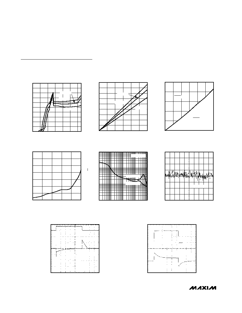
Typical Operating Characteristics
(V
IN
= V
OUT
+ 0.5V, C
IN
= C
OUT
= 2.2µF, C
CC
= 33nF, T
A
= +25∞C, unless otherwise noted.)
-0.4
-0.2
0
0.2
0.4
NORMALIZED OUTPUT VOLTAGE
vs. LOAD CURRENT
MAX8860 toc01
LOAD CURRENT (mA)
OUTPUT VOLTAGE (%)
0
150
200
50
100
250
300
V
OUT
NORMALIZED AT I
OUT
= 0
-0.3
-0.1
-0.2
0
0.2
0.1
0.3
NORMALIZED OUTPUT VOLTAGE
vs. TEMPERATURE
MAX8860 toc02
TEMPERATURE (
∞C)
OUTPUT VOLTAGE (%)
-40
20
40
-20
0
60
80
I
OUT
= 0
I
OUT
= 100mA
I
OUT
= 200mA
V
OUT
NORMALIZED AT +25∞C, I
OUT
= 0
0
40
120
100
80
60
20
160
140
200
180
0
100
50
150
200
250
300
SUPPLY CURRENT vs. LOAD CURRENT
MAX8860 toc03
LOAD CURRENT (mA)
SUPPLY CURRENT (
µ
A)
T
A
= +85∞C
T
A
= +25∞C
T
A
= -40∞C
V
FAULT
= +3.6V
0.5
FAULT Output Off-Leakage Current
T
A
= +25∞C
T
A
= +85∞C
V
IL
, 2.5V
V
IN
5.5V
V
IH
, 2.5V
V
IN
5.5V
V
0.4
V
2.0
SHDN Input Threshold
C
OUT
= 2.2µF
C
OUT
= 10µF
I
OUT
= 10mA,
10Hz < f < 100kHz
C
OUT
= 100µF
10Hz < f < 100kHz, C
OUT
= 10µF
µV
RMS
190
55
Output Voltage Noise
nV
Hz
Output Voltage Noise Density
MAX8860
Low-Dropout, 300mA
Linear Regulator in µMAX
4
_______________________________________________________________________________________
Typical Operating Characteristics (continued)
(V
IN
= V
OUT
+ 0.5V, C
IN
= C
OUT
= 2.2µF, C
CC
= 33nF, T
A
= +25∞C, unless otherwise noted.)
0
60
40
20
100
80
180
160
140
120
200
0
1
2
3
4
5
6
NO LOAD SUPPLY CURRENT
vs. INPUT VOLTAGE
MAX8860 toc04
INPUT VOLTAGE (V)
SUPPLY CURRENT (
µ
A)
T
A
= +85
∞C
T
A
= +25
∞C
T
A
= -40
∞C
20
60
40
120
100
80
160
0
140
180
0
100
50
150
200
250
300
DROPOUT VOLTAGE vs. LOAD CURRENT
MAX8860 toc05
LOAD CURRENT (mA)
DROPOUT VOLTAGE (mV)
T
A
= +85
∞C
T
A
= +25
∞C
T
A
= -40
∞C
0
50
150
100
200
250
0
100
50
150
200
250
300
FAULT DETECT THRESHOLD
vs. LOAD CURRENT
MAX8860 toc06
LOAD CURRENT (mA)
FAULT DETECT THRESHOLD (mV)
FAULT = HIGH
FAULT = LOW
-70
-50
-60
-30
-40
-10
-20
0
0.01
1
0.1
10
100
1000
POWER-SUPPLY REJECTION RATIO
vs. FREQUENCY
MAX8860 toc07
FREQUENCY (kHz)
PSRR (dB)
200mA
I
LOAD
0
LOAD-TRANSIENT RESPONSE
MAX8860 toc10
400
µs/div
V
OUT
20mV/div
V
IN
= V
OUT
+ 200mV
0.1
10
1
100
1000
OUTPUT NOISE SPECTRAL DENSITY
MAX8860 toc08
FREQUENCY (kHz)
NOISE (
µ
V/
Hz)
0.01
0.1
1.0
10
C
OUT
= 2.2
µF
C
OUT
= 10
µF
I
LOAD
= 10mA
V
OUT
500
µV/div
OUTPUT NOISE
(10Hz TO 1MHz)
MAX8860 toc09
1ms/div
I
LOAD
= 200mA
+4.3V
LINE-TRANSIENT RESPONSE
MAX8860 toc12
500
µs/div
V
OUT
2mV/div
V
IN
+3.3V
I
LOAD
= 200mA
MAX8860
Low-Dropout, 300mA
Linear Regulator in µMAX
_______________________________________________________________________________________
5
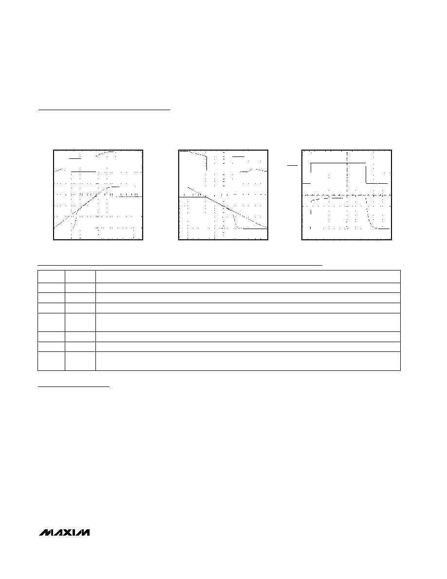
Typical Operating Characteristics (continued)
(V
IN
= V
OUT
+ 0.5V, C
IN
= C
OUT
= 2.2µF, C
CC
= 33nF, T
A
= +25∞C, unless otherwise noted.)
NAME
FUNCTION
1, 4
OUT
Regulator Output. Bypass with 2.2µF, low-ESR capacitor to GND for stable operation.
PIN
Pin Description
4V
2V
0
4V
3V
2V
1V
0
POWER-UP RESPONSE
MAX8860 toc13
5ms/div
FAULT
V
OUT
V
IN
4V
2V
0
4V
3V
2V
1V
0
POWER-DOWN RESPONSE
MAX8860 toc14
2ms/div
V
OUT
V
IN
FAULT
4V
2V
0
3V
2V
1V
0
SHUTDOWN/POWER-UP
MAX8860 toc15
400
µs/div
V
OUT
SHDN
2
IN
Supply Input. Connect to power source (+2.5V to +6.5V). Bypass with 2.2µF capacitor to GND.
3
GND
Ground
5
SET
Output Voltage Set. Connect to GND for internally set threshold. Connect to resistor-divider for adjustable
output voltages. See Output Voltage Selection section for more information.
6
CC
Compensation Capacitor. Connect a 0.033µF capacitor from CC to GND.
7
SHDN
Shutdown Input. Connect to IN for normal operation. Drive SHDN low to turn off the regulator.
8
FAULT
Fault Output. A high-impedance, open-drain output. When the MAX8860 is out of regulation, FAULT goes
low. In shutdown, the FAULT pin is high impedance. Connect to GND if unused.
Detailed Description
The MAX8860 is a low-dropout, low-quiescent-current
linear regulator designed primarily for battery-powered
applications. It supplies an adjustable +1.25V to
+6.5V output voltage or a fixed-voltage output of +1.8V
(MAX8860EUA18), +2.5V (MAX8860EUA25), +2.77V
(MAX8860EUA27), +2.82V (MAX8860EUA28), +3.0V
(MAX8860EUA30), or +3.3V (MAX8860EUA33) for load
currents up to 300mA. The devices with 2.77V and
2.82V nominal outputs are designed to guarantee mini-
mum output voltages of 2.70V and 2.75V, respectively.
The device consists of a +1.25V reference, error amplifi-
er, MOSFET driver, P-channel pass transistor, Dual
Mode comparator, fault detector, and internal-feedback
voltage divider (Figure 1).
The 1.25V bandgap reference is connected to the error
amplifier's inverting input. The error amplifier compares
this reference to the selected feedback voltage and
amplifies the difference. The MOSFET driver reads the
error signal and applies the appropriate drive to the P-
channel pass transistor. If the feedback voltage is lower
than the reference voltage, the pass-transistor gate is
pulled lower, allowing more current to pass and
increasing the output voltage. If the feedback voltage
is higher than the reference voltage, the pass-transistor
gate is driven higher, allowing less current to pass to
the output. The output voltage is fed back through
either an internal resistor voltage divider connected to
OUT, or an external resistor network connected to SET.
The Dual Mode comparator examines V
SET
and selects
the feedback path. If V
SET
is below 60mV, internal
feedback is used and the output voltage is regulated to
the preset output voltage. Additional blocks include an
output current limiter, reverse battery protection, a ther-
mal sensor, a fault detector, and shutdown logic.