For free samples & the latest literature: http://www.maxim-ic.com, or phone 1-800-998-8800
_______________General Description
The MAX8865 and MAX8866 dual, low-dropout linear
regulators operate from a +2.5V to +5.5V input range
and deliver up to 100mA. At 200mA total load, the
PMOS pass transistors keep the supply current at
145µA, making these devices ideal for battery-operated
portable equipment such as cellular phones, cordless
phones, and modems.
The devices feature Dual ModeTM operation: their out-
put voltages are preset (at 3.15V for the "T" versions,
2.84V for the "S" versions, or 2.80V for the "R" versions)
or can be adjusted with external resistor dividers. Other
features include independent low-power shutdown,
short-circuit protection, thermal shutdown protection,
and reverse battery protection. The MAX8866 also
includes an auto-discharge function, which actively dis-
charges the selected output voltage to ground when
the device is placed in shutdown mode. Both devices
come in a miniature 8-pin µMAX package.
________________________Applications
Cordless Telephones
Modems
PCS Telephones
Hand-Held Instruments
Cellular Telephones
Palmtop Computers
PCMCIA Cards
Electronic Planners
____________________________Features
o
Low Cost
o
Low, 55mV Dropout Voltage @ 50mA I
OUT
o
Low, 105µA No-Load Supply Current
o
Low, 145µA Operating Supply Current (even in
dropout)
o
Low, 350µV
RMS
Output Noise
o
Independent, Low-Current Shutdown Control
o
Thermal Overload Protection
o
Output Current Limit
o
Reverse Battery Protection
o
Dual Mode Operation: Fixed or Adjustable (1.25V
to 5.5V) Outputs
MAX8865T/S/R, MAX8866T/S/R
Dual, Low-Dropout, 100mA Linear Regulators
________________________________________________________________
Maxim Integrated Products
1
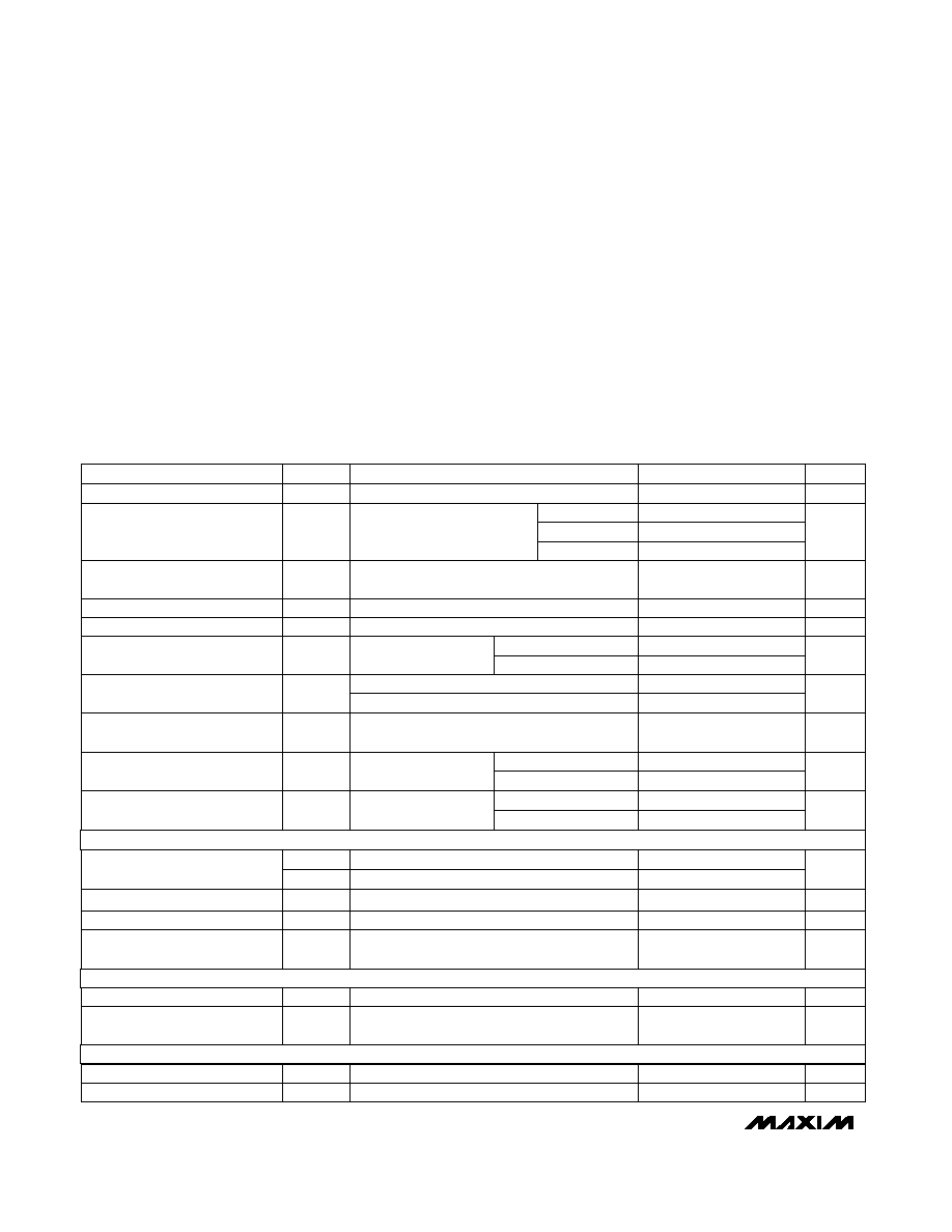
TOP VIEW
1
2
3
4
8
7
6
5
SET1
SHDN1
SHDN2
SET2
OUT2
GND
IN
OUT1
MAX8865
MAX8866
µ
MAX
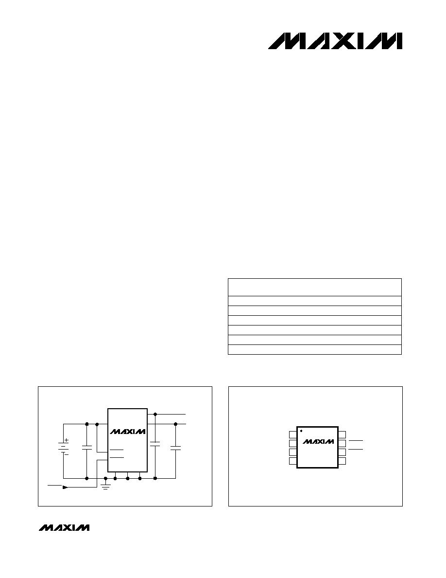
__________________Pin Configuration
MAX8865
MAX8866
OUT1
OUT2
GND
SET2
SET1
IN
SHDN1
C
OUT2
1
µ
F
C
OUT1
1
µ
F
C
IN
2
µ
F
BATTERY
OUTPUT
VOLTAGE 2
OUTPUT
VOLTAGE 1
SHDN2
SHDN2
__________Typical Operating Circuit
19-0485; Rev 0; 4/96
PART
MAX8865
TEUA
MAX8865SEUA
MAX8866
TEUA
-40∞C to +85∞C
-40∞C to +85∞C
-40∞C to +85∞C
TEMP. RANGE
PIN-
PACKAGE
8 µMAX
8 µMAX
8 µMAX
______________Ordering Information
PRESET
V
OUT
(V)
3.15
2.84
3.15
MAX8866SEUA
-40∞C to +85∞C
8 µMAX
2.84
Dual Mode is a trademark of Maxim Integrated Products.
MAX8865REUA
-40∞C to +85∞C
8 µMAX
2.80
MAX8866REUA
-40∞C to +85∞C
8 µMAX
2.80
MAX8865T/S/R, MAX8866T/S/R
Dual, Low-Dropout, 100mA Linear Regulators
2
_______________________________________________________________________________________
ABSOLUTE MAXIMUM RATINGS
ELECTRICAL CHARACTERISTICS
(V
IN
= +3.6V, GND = 0V, T
A
= 0∞C to +85∞C, unless otherwise noted. Typical values are at T
A
= +25∞C.)
Stresses beyond those listed under "Absolute Maximum Ratings" may cause permanent damage to the device. These are stress ratings only, and functional
operation of the device at these or any other conditions beyond those indicated in the operational sections of the specifications is not implied. Exposure to
absolute maximum rating conditions for extended periods may affect device reliability.
V
IN
to GND ..................................................................-6V to +6V
Output Short-Circuit Duration ............................................Infinite
SET_ to GND ............................................................-0.3V to +6V
SHDN_
_ to GND ............................................................-6V to +6V
SHDN_
_ to IN .............................................................-6V to +0.3V
OUT_ to GND...............................................-0.3V to (V
IN
+ 0.3V)
Continuous Power Dissipation (T
A
= +70∞C)
µMAX (derate 4.1mW/∞C above +70∞C)......................330mW
Operating Temperature Range ...........................-40∞C to +85∞C
Junction Temperature ......................................................+150∞C
Thermal Resistance (
JA
)...............................................244∞C/W
Storage Temperature Range .............................-65∞C to +160∞C
Lead Temperature (soldering, 10sec) .............................+300∞C
ms
1
Shutdown to Output
Discharge Delay (MAX8866)
0
1000
I
SHDN_
_
SHDN Input Bias Current
V
0.4
V
IL
SHDN Input Threshold
2.0
V
IH
µV
RMS
220
Output Voltage Noise
350
0.012
0.03
%/V
-0.10
0
0.10
V
LNR
Line Regulation
mV
55
120
Dropout Voltage (Note 4)
V
2.5
5.5
V
IN
Input Voltage (Note 1)
1.1
3.08
3.15
3.24
V
V
SET_
5.5
V
OUT_
Adjustable Output Voltage
Range (Note 2)
mA
100
Maximum Output Current
UNITS
MIN
TYP
MAX
SYMBOL
PARAMETER
C
OUT
= 1µF, no load
V
SHDN_
_
= V
IN
V
IN
= 2.5V to 5.5V, SET_ tied to OUT_,
I
OUT_
= 1mA
I
OUT
= 50mA
CONDITIONS
mA
220
I
LIM
Current Limit (Note 3)
MAX886_T
10Hz to 1MHz
I
OUT
= 1mA
MAX886_S
2.77
2.84
2.91
105
270
0.16
3000
nA
I
Q
SHDN
Shutdown Supply Current
V
OUT_
= 0V
nA
1.222
1.25
1.276
V
SET_
V
IN
= 2.5V to 5.5V, I
OUT_
= 1mA
SET Reference Voltage (Note 2)
V
0.015
50
I
SET_
V
SET_
= 1.3V
SET Input Leakage Current
(Note 2)
nA
170
T
SHDN
Thermal Shutdown Temperature
∞C
20
T
SHDN
Thermal Shutdown Hysteresis
∞C
145
SET_ = GND
µA
I
Q
Ground Pin Current
I
OUT_
= 0mA to 50mA
%/mA
0.006
V
LDR
Load Regulation
I
OUT_
= 50mA
I
OUT_
= 0mA
MAX886_R
V
2.73
2.80
2.87
V
OUT_
Output Voltage
0mA
I
OUT
50mA,
SET_ = GND
SHUTDOWN
THERMAL PROTECTION
SET INPUT
SET_ = GND
SET_ tied to OUT_
C
OUT
= 1µF
C
OUT
= 100µF
MAX8865T/S/R, MAX8866T/S/R
Dual, Low-Dropout, 100mA Linear Regulators
_______________________________________________________________________________________
3
ELECTRICAL CHARACTERISTICS
(V
IN
= +3.6V, GND = 0V, T
A
= -40∞C to +85∞C, unless otherwise noted. Typical values are at T
A
= +25∞C.) (Note 5)
Note 1:
Guaranteed by line regulation test.
Note 2:
Adjustable mode only.
Note 3:
Not tested. For design purposes, the current limit should be considered 120mA minimum to 320mA maximum.
Note 4:
The dropout voltage is defined as (V
IN_
- V
OUT_
) when V
OUT_
is 100mV below the value of V
OUT_
for V
IN_
= V
OUT_
+2V.
Note 5:
Specifications to -40∞C are guaranteed by design and not production tested.
MAX886_S
2.74
2.84
2.93
1.207
1.25
1.288
105
270
nA
MAX886_T
0.16
3000
I
OUT
= 1mA
nA
I
Q
SHDN
mA
Shutdown Supply Current
220
V
SET_
V
OUT_
= 0V
I
LIM
ms
1
Shutdown to Output
Discharge Delay (MAX8866)
V
IN
= 2.5V to 5.5V, I
OUT_
= 1mA
SET Reference Voltage (Note 2)
0
1000
V
0.015
50
20
I
SHDN_
_
SHDN Input Bias Current
µV
RMS
220
Output Voltage Noise
T
SHDN
350
I
SET_
V
SET_
= 1.3V
SET Input Leakage Current
(Note 2)
Thermal Shutdown Hysteresis
∞C
nA
0.012
0.03
%/V
-0.11
0
0.11
V
LNR
Line Regulation
170
T
SHDN
mV
55
120
Dropout Voltage (Note 4)
Thermal Shutdown Temperature
∞C
V
2.5
5.5
V
IN
Input Voltage (Note 1)
1.1
µA
3.05
3.15
3.26
V
V
SET_
5.5
V
OUT_
Adjustable Output Voltage
Range (Note 2)
mA
80
Maximum Output Current
UNITS
MIN
TYP
MAX
SYMBOL
PARAMETER
C
OUT
= 1µF
V
SHDN_
_
= V
IN
10Hz to 1MHz
V
IN
= 2.5V to 5.5V,
SET_ tied to OUT_, I
OUT_
= 1mA
I
OUT
= 50mA
CONDITIONS
Current Limit (Note 3)
145
SET_ = GND
I
Q
Ground Pin Current
%/mA
0.006
V
LDR
Load Regulation
I
OUT_
= 50mA
I
OUT_
= 0mA
I
OUT_
= 0mA to 50mA
SET_ = GND
SET_ tied to OUT_
V
0.4
V
IL
SHDN Input Threshold
2.0
V
IH
C
OUT
= 1µF
C
OUT
= 100µF
MAX886_R
V
2.70
2.80
2.89
V
OUT_
Output Voltage
0mA
I
OUT
50mA,
SET_ = GND
SHUTDOWN
SET INPUT
THERMAL PROTECTION

MAX8865T/S/R, MAX8866T/S/R
Dual, Low-Dropout, 100mA Linear Regulators
4
_______________________________________________________________________________________
__________________________________________Typical Operating Characteristics
(V
IN
= +3.6V, C
IN
= 2µF, C
OUT
= 1µF,
SHDN2 = GND, MAX886_S, T
A
= +25∞C, unless otherwise noted.)
3.00
2.70
0
20 30
10
60 70
100
OUTPUT VOLTAGE
vs. LOAD CURRENT
2.75
2.95
2.90
MAX8865/66-01
LOAD CURRENT (mA)
OUTPUT VOLTAGE (V)
40 50
80 90
2.85
2.80
V
OUT1
180
0
20
10
60 70
100
SUPPLY CURRENT
vs. LOAD CURRENT
140
160
120
MAX8865/66-02
LOAD CURRENT (mA)
SUPPLY CURRENT (
µ
A)
30 40 50
80 90
100
60
80
SHDN2
= V
IN
, I
LOAD2
= 50mA
SHDN2
= GND
3.5
0
0
1
4
6
OUTPUT VOLTAGE
vs. INPUT VOLTAGE
1.0
0.5
3.0
2.5
MAX8865/66-03
INPUT VOLTAGE (V)
OUTPUT VOLTAGE (V)
2
3
5
2.0
1.5
V
OUT1
NO LOAD
100
0
0
1
4
6
SUPPLY CURRENT
vs. INPUT VOLTAGE
30
20
10
80
90
70
MAX8865/66-04
INPUT VOLTAGE (V)
SUPPLY CURRENT (
µ
A)
2
3
5
60
40
50
I
LOAD1
=
50mA
I
LOAD1
= 0mA
ONE REGULATOR ENABLED, NO LOAD
180
60
-40
-20
40
80
SUPPLY CURRENT
vs. TEMPERATURE
100
80
160
140
MAX8865/66-07
TEMPERATURE (∞C)
SUPPLY CURRENT (
µ
A)
0
20
60
120
SHDN2 = V
IN
I
LOAD1
= I
LOAD2
= 50mA
SHDN2 = GND
I
LOAD1
= 50mA
200
0
0
1
4
6
TOTAL SUPPLY CURRENT
vs. INPUT VOLTAGE
60
40
20
160
180
140
MAX8865/66-05
INPUT VOLTAGE (V)
SUPPLY CURRENT (
µ
A)
2
3
5
120
80
100
I
LOAD1
= I
LOAD2
=
50mA
I
LOAD1
= I
LOAD2
= 0mA
SHDN1 = SHDN2 = V
IN
3.0
2.7
-40
-20
40
80
OUTPUT VOLTAGE
vs. TEMPERATURE
2.8
MAX8865/66-06
TEMPERATURE (∞C)
OUTPUT VOLTAGE (V)
0
20
60
2.9
0
60
40
20
80
100
120
140
0
20
60
100
DROPOUT VOLTAGE
vs. LOAD CURRENT
MAX8865/66-08
LOAD CURRENT (mA)
DROPOUT VOLTAGE (mV)
40
80
10
30
70
50
90
T
A
= +85∞C
T
A
= +25∞C
T
A
= -40∞C
1
10
MAX8865/66-09
FREQUENCY (kHz)
PSRR (dB)
80
70
60
50
40
30
10
20
0
100
1000
0.10
0.01
V
OUT
= 2.84V
R
L
= 55
C
OUT
= 10
µ
F
C
OUT
= 1
µ
F
POWER-SUPPLY REJECTION RATIO
vs. FREQUENCY
MAX8865T/S/R, MAX8866T/S/R
Dual, Low-Dropout, 100mA Linear Regulators
_______________________________________________________________________________________
5
10
0.01
0.1
10
100
1
1000
OUTPUT SPECTRAL NOISE DENSITY
vs. FREQUENCY
0.1
MAX8865/66-10
FREQUENCY (kHz)
OUTPUT SPECTRAL NOISE DENSITY (
µ
V/Hz)
1
R
L
= 55
C
OUT
= 1µF
C
OUT
= 100µF
1000
0.01
0
50 60 70 80 90
10 20 30 40
100
REGION OF STABLE C
OUT
ESR
vs. LOAD CURRENT
0.1
MAX8865/66-11
LOAD CURRENT (mA)
C
OUT
ESR (
)
1
10
100
INTERNAL FEEDBACK
STABLE REGION
C
OUT
= 1µF
EXTERNAL FEEDBACK
I
LOAD
= 50mA, V
OUT
IS AC COUPLED
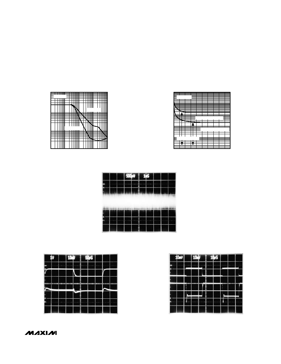
LINE-TRANSIENT RESPONSE
4.6V
3.6V
2.84V
2.82V
2.83V
50
µ
s/div
V
IN
V
OUT
I
LOAD
= 50mA, V
OUT
IS AC COUPLED
OUTPUT NOISE DC TO 1MHz
V
OUT
1ms/div
V
IN
= 3.60V, I
LOAD
= 0mA to 50mA, C
IN
= 10
µ
F, V
OUT
IS AC COUPLED
LOAD-TRANSIENT RESPONSE
I
LOAD
10
µ
s/div
V
OUT
50mA
0mA
2.85V
2.84V
2.83V
____________________________Typical Operating Characteristics (continued)
(V
IN
= +3.6V, C
IN
= 2µF, C
OUT
= 1µF,
SHDN2 = GND, MAX886_S, T
A
= +25∞C, unless otherwise noted.)