General Description
The MAX9382/MAX9383 are high-speed PECL/ECL
phase-frequency detectors designed for use in high-
bandwidth phase-locked loop (PLL) applications. The
devices compare a single-ended reference (R) and a
VCO (V) input and produce pulse streams on differen-
tial up (U) and down (D) outputs. When integrated, the
difference of the output pulse streams provides a con-
trol voltage proportional to input phase or frequency dif-
ference. Guaranteed minimum short pulse duration
completely eliminates minimum phase difference
requirements during the lock condition, maximizing
loop jitter performance.
The MAX9382/MAX9383 feature low propagation and
reset delay, making them ideal for high-frequency clock
synchronization use. The MAX9382 uses 100K logic
levels, has a supply voltage range of V
CC
- V
EE
= 4.2V
to 5.5V, and is pin compatible with Motorola's
MCK12140. The MAX9383 uses 10H logic levels with a
supply voltage range of V
CC
- V
EE
= 4.75V to 5.5V and
is pin compatible with the MCH12140.
The MAX9382/MAX9383 are available in industry-stan-
dard 8-pin SO and space-saving 8-pin µMAX packages.
Applications
Precision Clock Distribution
Central Office
DSLAM
DLC
Base Station
ATE
Features
o Guaranteed Minimum Pulse Width Eliminates
Dead Band
o 450MHz Typical Bandwidth with up to ± Phase
Detection
o 75k Internal Input Pulldown Resistors
o 44mA Typical Supply Current
o ±2kV ESD Protection (Human Body Model)
o Pin Compatible with MCK12140 and MCH12140
o Available in 8-Pin µMAX and SO Packages
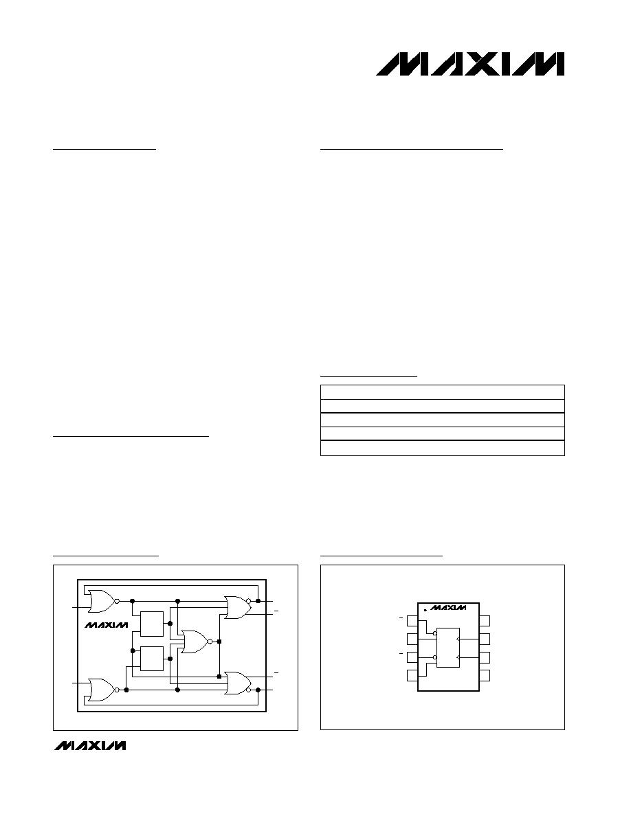
MAX9382/MAX9383
ECL/PECL Phase-Frequency Detectors
________________________________________________________________ Maxim Integrated Products
1
V
V
EE
D
1
2
8
7
V
CC
R
U
D
U
µMAX/SO
TOP VIEW
3
4
6
5
MAX9382
MAX9383
Pin Configuration
Ordering Information
19-2234; Rev 1; 11/02
*Future product--contact factory for availability.
For pricing, delivery, and ordering information, please contact Maxim/Dallas Direct! at
1-888-629-4642, or visit Maxim's website at www.maxim-ic.com.
PART
TEMP RANGE
PIN-PACKAGE
MAX9382EUA*
-40∞C to +85∞C
8 µMAX
MAX9382ESA
-40∞C to +85∞C
8 SO
MAX9383EUA*
-40∞C to +85∞C
8 µMAX
MAX9383ESA
-40∞C to +85∞C
8 SO
D
U
D
U
R
R
V
R
Q
Q
S
S
MAX9382
MAX9383
Functional Diagram
MAX9382/MAX9383
ECL/PECL Phase-Frequency Detectors
2
_______________________________________________________________________________________
ABSOLUTE MAXIMUM RATINGS
MAX9382 DC ELECTRICAL CHARACTERISTICS
(V
CC
- V
EE
= 4.2V to 5.5V. Outputs loaded with 50
±1% to V
CC
- 2V, unless otherwise noted. Typical values at V
CC
- V
EE
= 4.5V.)
(Notes 1, 2, 3)
Stresses beyond those listed under "Absolute Maximum Ratings" may cause permanent damage to the device. These are stress ratings only, and functional
operation of the device at these or any other conditions beyond those indicated in the operational sections of the specifications is not implied. Exposure to
absolute maximum rating conditions for extended periods may affect device reliability.
V
CC
- V
EE
............................................................................+6.0V
Inputs (R, V).................................................(V
CC
) to (V
EE
- 0.3V)
Continuous Output Current .................................................50mA
Surge Output Current........................................................100mA
Junction-to-Ambient Thermal Resistance in Still Air*
8-Pin µMAX ..............................................................+221∞C/W
8-Pin SO ..................................................................+170∞C/W
Junction-to-Ambient Thermal Resistance with*
500LFPM Airflow
8-Pin µMAX ..............................................................+155∞C/W
8-Pin SO.....................................................................+99∞C/W
Junction-to-Case Thermal Resistance
8-Pin µMAX ...............................................................+39∞C/W
8-Pin SO....................................................................+40∞C/W
Operating Temperature Range ...........................-40∞C to +85∞C
Junction Temperature ......................................................+150∞C
Storage Temperature Range .............................-65∞C to +150∞C
ESD Protection
Human Body Model (R, V, U, U, D, D)............................±2kV
Soldering Temperature (10s) .......................................... +300∞C
*Ratings are for single-layer board.
-40
∞C
+25
∞C
+85
∞C
PARAMETER
SYMBOL CONDITIONS
MIN
TYP
MAX
MIN
TYP
MAX
MIN
TYP
MAX
UNITS
INPUTS (R, V)
Input High
Voltage
V
IH
V
CC
-
1.165
V
CC
-
0.880
V
CC
-
1.165
V
CC
-
0.880
V
CC
-
1.165
V
CC
-
0.880
V
Input Low
Voltage
V
IL
V
CC
-
1.810
V
CC
-
1.475
V
CC
-
1.810
V
CC
-
1. 475
V
CC
-
1.810
V
CC
-
1.475
V
Input High
Current
I
IH
V
IN
= V
IHMAX
150
150
150
µA
Input Low
Current
I
IL
V
IN
= V
ILMIN
0.5
0.5
0.5
µA
OUTPUTS (U,
U, D, D)
Single-Ended
Output High
Voltage
V
OH
V
IN
= V
IH
or
V
IL
V
CC
-
1.085
V
CC
-
0.990
V
CC
-
0.880
V
CC
-
1.035
V
CC
-
0.960
V
CC
-
0.880
V
CC
-
1.035
V
CC
-
0.940
V
CC
-
0.880
V
Single-Ended
Output Low
Voltage
V
OL
V
IN
= V
IH
or
V
IL
V
CC
-
1.890
V
CC
-
1.810
V
CC
-
1.555
V
CC
-
1.850
V
CC
-
1.770
V
CC
-
1.620
V
CC
-
1.810
V
CC
-
1.730
V
CC
-
1.600
V
Differential
Output Voltage
V
OH
-
V
OL
V
IN
= V
IH
or
V
IL
585
820
585
810
585
800
mV
POWER SUPPLY
Supply Current
I
EE
(Note 4)
43
56
44
56
45
58
mA
MAX9382/MAX9383
ECL/PECL Phase-Frequency Detectors
_______________________________________________________________________________________
3
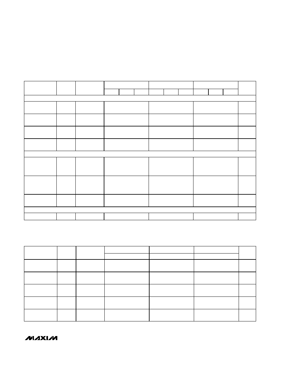
MAX9383 DC ELECTRICAL CHARACTERISTICS
(V
CC
- V
EE
= 4.75V to 5.5V. Outputs loaded with 50
±1% to V
CC
- 2V, unless otherwise noted. Typical values at V
CC
- V
EE
= 5.2V.)
(Notes 1, 2, 3)
MAX9382/MAX9383 AC ELECTRICAL CHARACTERISTICS
(Over specified DC input parameters, f = 100MHz, outputs loaded with 50
±1% to V
CC
- 2V, unless otherwise noted.) (Note 5)
-40
∞C
+25
∞C
+85
∞C
PARAMETER
SYMBOL CONDITIONS
MIN
TYP
MAX
MIN
TYP
MAX
MIN
TYP
MAX
UNITS
INPUTS (R, V)
Input High
Voltage
V
IH
V
CC
-
1.230
V
CC
-
0.890
V
CC
-
1.130
V
CC
-
0.810
V
CC
-
1.060
V
CC
-
0.720
V
Input Low
Voltage
V
IL
V
CC
-
1.950
V
CC
-
1.500
V
CC
-
1.950
V
CC
-
1. 480
V
CC
-
1.950
V
CC
-
1.480
V
Input High
Current
I
IH
V
IN
= V
IHMAX
150
150
150
µA
Input Low
Current
I
IL
V
IN
= V
ILMIN
0.5
0.5
0.5
µA
OUTPUTS (U,
U, D, D)
Single-Ended
Output High
Voltage
V
OH
V
IN
= V
IH
or
V
IL
V
CC
-
1.115
V
CC
-
1.010
V
CC
-
0.890
V
CC
-
0.980
V
CC
-
0.924
V
CC
-
0.810
V
CC
-
0.945
V
CC
-
0.900
V
CC
-
0.720
V
Single-Ended
Output Low
Voltage
V
OL
V
IN
= V
IH
or
V
IL
V
CC
-
1.990
V
CC
-
1.832
V
CC
-
1.650
V
CC
-
1.950
V
CC
-
1.740
V
CC
-
1.630
V
CC
-
1.950
V
CC
-
1.700
V
CC
-
1.595
V
Differential
Output Voltage
V
OH
-
V
OL
V
IN
= V
IH
or
V
IL
650
822
650
817
650
803
mV
POWER SUPPLY
Supply Current
I
EE
(Note 4)
37
52
38
52
39
52
mA
-40
∞C
+25
∞C
+85
∞C
PARAMETER
SYMBOL CONDITIONS
MIN
TYP
MAX
MIN
TYP
MAX
MIN
TYP
MAX
UNITS
R Input to U
Output Delay
t
PRU
Figure 1
575
650
750
590
660
780
635
720
830
ps
V Input to D
Output Delay
t
PVD
Figure 1
575
650
750
590
660
780
635
720
830
ps
R Input to D
Output Delay
t
PRD
Figure 1
945
1120
1320
960
1110
1360
1005
1150
1360
ps
V Input to U
Output Delay
t
PVU
Figure 1
945
1120
1320
960
1110
1360
1005
1150
1360
ps
Minimum Pulse
Duration
t
Pmin
Figure 1
370
470
370
450
370
430
ps
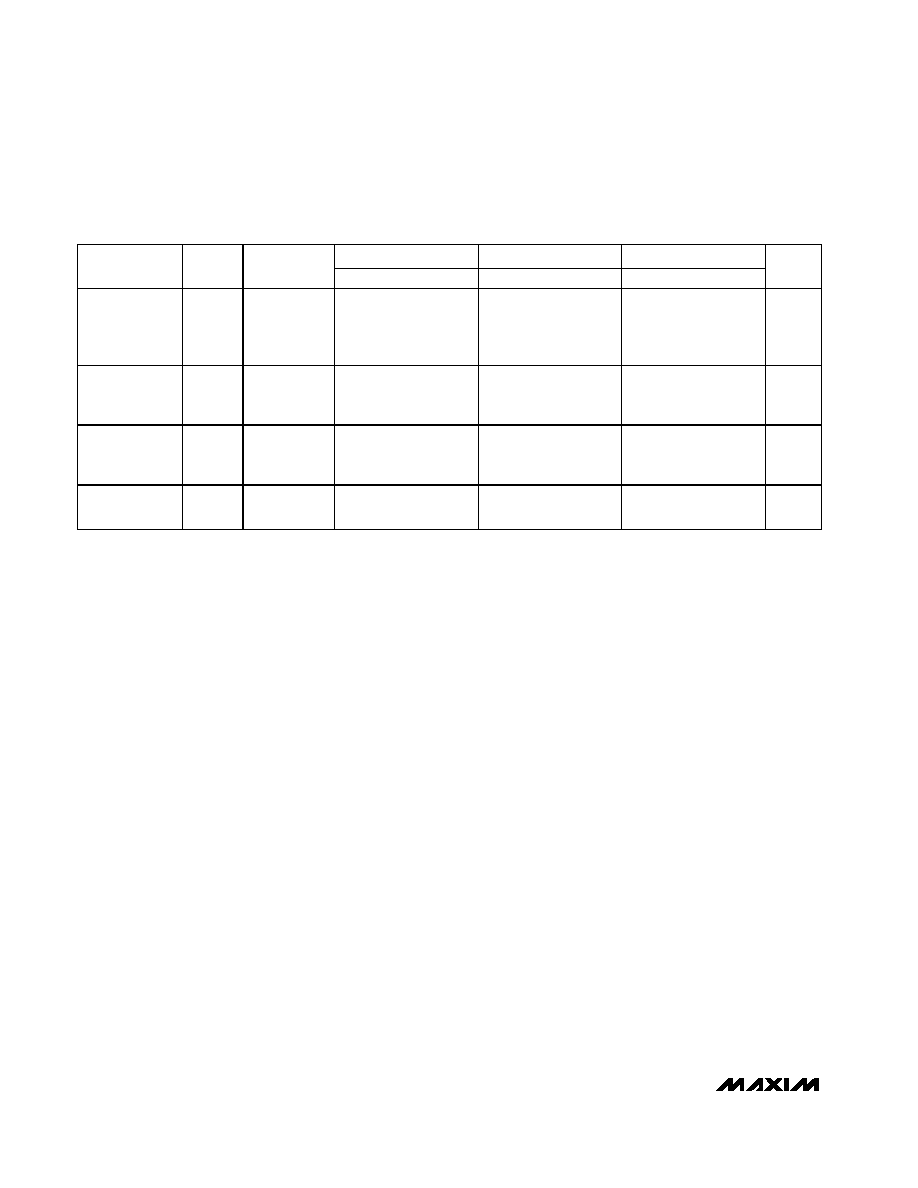
MAX9382/MAX9383
ECL/PECL Phase-Frequency Detectors
4
_______________________________________________________________________________________
-40
∞C
+25
∞C
+85
∞C
PARAMETER
SYMBOL
CONDITIONS
MIN
TYP
MAX
MIN
TYP
MAX
MIN
TYP
MAX
UNITS
Maximum
Operating
Frequency
f
MAX
± usable
phase
difference
range
400
450
400
450
400
450
MHz
Phase Offset
V
IN
= 200MHz,
50% duty
cycle (Note 6)
30
70
28
60
28
60
ps
Added Random
Jitter
t
RJ
V
IN
= 400MHz,
50% duty
cycle (Note 7)
0.2
1.0
0.2
1.0
0.2
1.0
ps
(RMS)
Output Rise/ Fall
Time
t
R
, t
F
20% to 80%,
Figure 2
80
160
100
180
110
190
ps
Note 1: Measurements are made with the device in thermal equilibrium.
Note 2: Current into a pin is defined as positive. Current out of a pin is defined as negative.
Note 3: DC parameters are production tested at +85∞C. DC limits are guaranteed by design and characterization over the full oper-
ating temperature range.
Note 4: All pins open except V
CC
and V
EE
.
Note 5: Guaranteed by design and characterization. Limits are set to ±6 sigma.
Note 6: Phase offset is defined as the difference in propagation delay timing between the two input paths. It is measured between
the U and D outputs at the differential crosspoint with a rising edge simultaneously applied at the R and V inputs.
Note 7: Device jitter added to the input signal.
MAX9382/MAX9383 AC ELECTRICAL CHARACTERISTICS (continued)
(Over specified DC input parameters, f = 100MHz, outputs loaded with 50
±1% to V
CC
- 2V, unless otherwise noted.) (Note 5)
MAX9382/MAX9383
ECL/PECL Phase-Frequency Detectors
_______________________________________________________________________________________
5
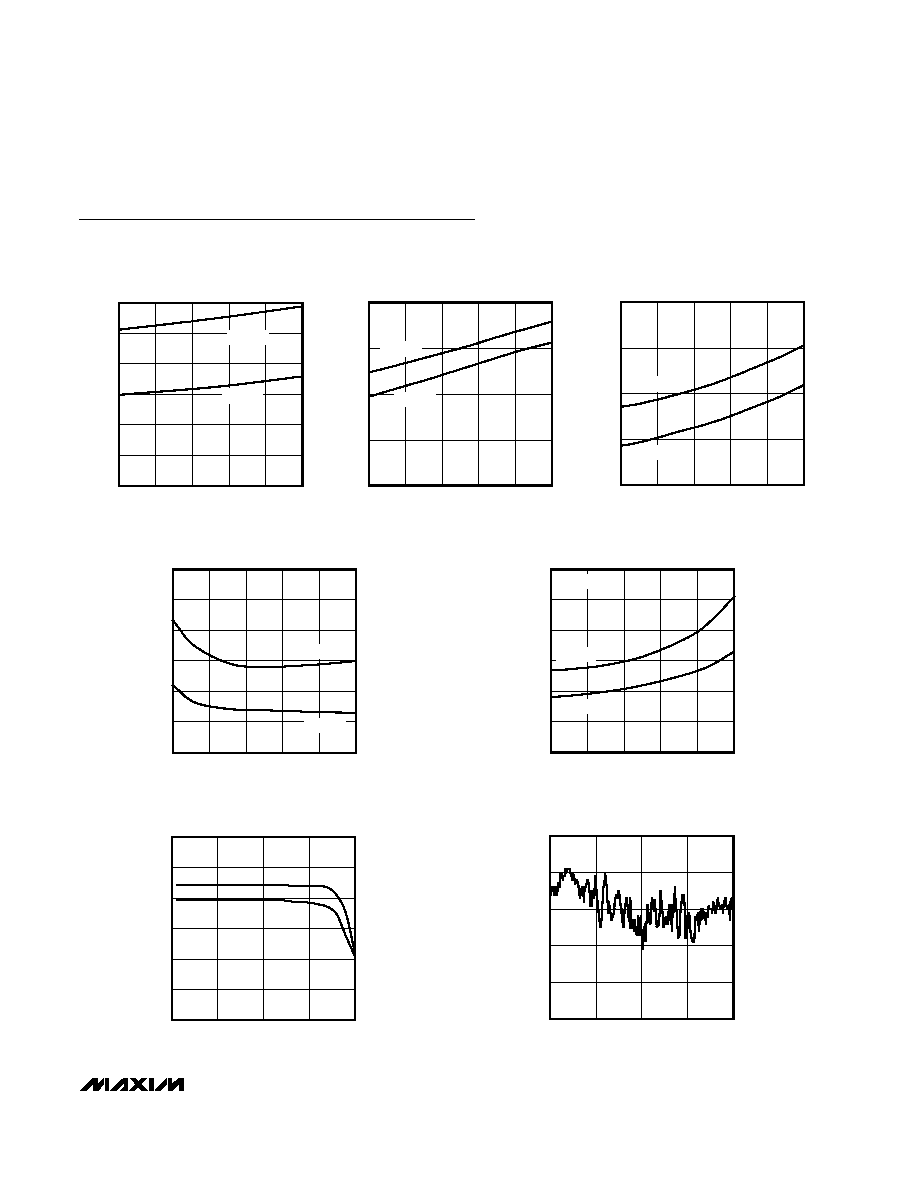
30.0
35.0
32.5
40.0
37.5
42.5
45.0
-40
35
-15
10
60
85
SUPPLY CURRENT vs. TEMPERATURE
MAX9382/83 toc01
TEMPERATURE (
∞C)
SUPPLY CURRENT (mA)
MAX9382
MAX9383
50
75
100
125
150
-40
10
-15
35
60
85
MAX9382
TRANSITION TIME vs. TEMPERATURE
MAX9382/83 toc02
TEMPERATURE (
∞C)
TRANSITION TIME (ps)
RISE TIME
FALL TIME
100
125
150
175
200
-40
10
-15
35
60
80
MAX9383
TRANSITION TIME vs. TEMPERATURE
MAX9382/83 toc03
TEMPERATURE (
∞C)
TRANSITION TIME (ps)
RISE TIME
FALL TIME
400
425
500
475
525
550
-40
10
-15
35
60
80
OUTPUT SHORT-PULSE DURATION
vs. TEMPERATURE
MAX9382/83 toc04
TEMPERATURE (
∞C)
OUTPUT SHORT-PULSE DURATION (ps)
MAX9382
MAX9383
450
600
650
625
700
675
725
750
-40
35
-15
10
60
85
PROPAGATION DELAY
vs. TEMPERATURE
MAX9382/83 toc05
TEMPERATURE (
∞C)
PROPAGATION DELAY (ps)
MAX9383
MAX9382
t
PRU
OR t
PVD
DIFFERENTIAL OUTPUT VOLTAGE
vs. FREQUENCY
MAX9382/83 toc06
FREQUENCY (MHz)
DIFFERENTIAL OUTPUT VOLTAGE (V)
1500
1000
500
780
790
800
810
820
830
770
0
2000
MAX9383
MAX9382
0
10
30
20
40
50
OUTPUT PHASE ERROR
vs. INPUT PHASE DIFFERENCE
MAX9382/83 toc07
INPUT PHASE DIFFERENCE (ns)
OUTPUT PHASE ERROR (ps)
-4
0
-2
2
4
Typical Operating Characteristics
(V
CC
- V
EE
= +4.5V (MAX9382) or V
CC
- V
EE
= +5.2V (MAX9383), V
IH
= V
CC
- 1.00V, V
IL
= V
CC
- 1.60V, f
R
= f
V
= 100MHz, outputs
loaded with 50
to V
CC
- 2V, T
A
= +25∞C, unless otherwise noted.)