General Description
The MAX9394/MAX9395 consist of a 2:1 multiplexer
and a 1:2 demultiplexer with loopback. The multiplexer
section (channel B) accepts two low-voltage differential
signaling (LVDS) inputs and generates a single LVDS
output. The demultiplexer section (channel A) accepts
a single LVDS input and generates two parallel LVDS
outputs. The MAX9394/MAX9395 feature a loopback
mode that connects the input of channel A to the output
of channel B and connects the selected input of chan-
nel B to the outputs of channel A.
Three LVCMOS/LVTTL logic inputs control the internal
connections between inputs and outputs, one for the
multiplexer portion of channel B (BSEL), and the other
two for loopback control of channels A and B (LB_SELA
and LB_SELB). Independent enable inputs for each dif-
ferential output pair provide additional flexibility.
Fail-safe circuitry forces the outputs to a differential low
condition for undriven inputs or when the common-
mode voltage exceeds the specified range. The
MAX9394 provides high-level input fail-safe detection
for HSTL, LVDS, and other GND-referenced differential
inputs. The MAX9395 provides low-level fail-safe detec-
tion for CML, LVPECL, and other V
CC
-referenced differ-
ential inputs.
Ultra low 91ps
P-P
(max) pseudorandom bit sequence
(PRBS) jitter ensures reliable communications in high-
speed links that are highly sensitive to timing error,
especially those incorporating clock-and-data recovery,
or serializers and deserializers. The high-speed switch-
ing performance guarantees 1.5GHz operation and less
than 87ps (max) skew between channels.
LVDS inputs and outputs are compatible with the
TIA/EIA-644 LVDS standard. The LVDS outputs drive
100
loads. The MAX9394/MAX9395 are offered in 32-
pin TQFP and 28-pin thin QFN packages and operate
over the extended temperature range (-40�C to +85�C).
Applications
High-Speed Telecom/Datacom Equipment
Central Office Backplane Clock Distribution
DSLAM
Protection Switching
Fault-Tolerant Systems
Features
o Guaranteed 1.5GHz Operation with 250mV
Differential Output Swing
o Simultaneous Loopback Control
o 2ps
(RMS)
(max) Random Jitter
o AC Specifications Guaranteed for 150mV
Differential Input
o Signal Inputs Accept Any Differential Signaling
Standard
o LVDS Outputs for Clock or High-Speed Data
o High-Level Input Fail-Safe Detection (MAX9394)
o Low-Level Input Fail-Safe Detection (MAX9395)
o +3.0V to +3.6V Supply Voltage Range
o LVCMOS/LVTTL Logic Inputs
MAX9394/MAX9395
2:1 Multiplexers and 1:2 Demultiplexers with
Loopback
________________________________________________________________ Maxim Integrated Products
1
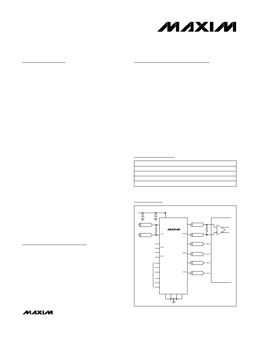
Ordering Information
0.1
�F
0.01
�F
+3.0V TO
+3.6V
OUTA0
OUTA0
LVDS
RECEIVER
INA
INA
ENA0
ENA1
ENB
GND
GND
GND
GND
OUTA1
OUTA1
OUTB
OUTB
LVCMOS/LVTTL
LOGIC INPUTS
LB_SELA
LB_SELB
BSEL
INB0
INB0
100
Z
0
= 50
Z
0
= 50
MAX9394
MAX9395
V
CC
INB1
INB1
Z
0
= 50
Z
0
= 50
100
Z
0
= 50
Z
0
= 50
Z
0
= 50
Z
0
= 50
Typical Operating Circuit
19-2878; Rev 0; 7/03
For pricing, delivery, and ordering information, please contact Maxim/Dallas Direct! at
1-888-629-4642, or visit Maxim's website at www.maxim-ic.com.
PART
TEMP RANGE
PIN-PACKAGE
MAX9394EHJ
-40�C to +85�C
32 TQFP
MAX9394ETI*
-40�C to +85�C
28 Thin QFN
MAX9395EHJ
-40�C to +85�C
32 TQFP
MAX9395ETI*
-40�C to +85�C
28 Thin QFN
*Future product--contact factory for availability.
Pin Configurations and Functional Diagram appear at end
of data sheet.

MAX9394/MAX9395
2:1 Multiplexers and 1:2 Demultiplexers with
Loopback
2
_______________________________________________________________________________________
ABSOLUTE MAXIMUM RATINGS
Stresses beyond those listed under "Absolute Maximum Ratings" may cause permanent damage to the device. These are stress ratings only, and functional
operation of the device at these or any other conditions beyond those indicated in the operational sections of the specifications is not implied. Exposure to
absolute maximum rating conditions for extended periods may affect device reliability.
V
CC
to GND ...........................................................-0.3V to +4.1V
IN_ _, IN_ _, OUT_ _, OUT_ _, EN_ _, _SEL, LB_SEL_
to GND........................................................-0.3V to (V
CC
+ 0.3V)
IN_ _ to IN_ _..........................................................................�3V
Short-Circuit Duration (OUT_ _, OUT_ _) ...................Continuous
Continuous Power Dissipation (T
A
= +70�C)
32-Pin TQFP (derate 13.1mW/�C above +70�C)........1047mW
28-Pin 5mm x 5mm Thin QFN
(derate 20.8mW/�C above +70�C) .............................1667mW
Junction-to-Ambient Thermal Resistance in Still Air
32-Pin TQFP............................................................+76.4�C/W
28-Pin 5mm x 5mm Thin QFN....................................+48�C/W
Junction-to-Case Thermal Resistance
28-Pin 5mm x 5mm Thin QFN......................................+2�C/W
Operating Temperature Range ...........................-40�C to +85�C
Junction Temperature ......................................................+150�C
Storage Temperature Range .............................-65�C to +150�C
ESD Protection (Human Body Model)
(IN_ _, IN_ _, OUT_ _, OUT_ _, EN_ _, SEL_, LB_SEL_) ..�2kV
Soldering Temperature (10s) ...........................................+300�C
DC ELECTRICAL CHARACTERISTICS
(V
CC
= +3.0V to +3.6V, R
L
= 100
�1%, EN_ _ = V
CC
, V
CM
= +0.05V to (V
CC
- 0.6V) (MAX9394), V
CM
= +0.06V to (V
CC
- 0.05V)
(MAX9395), T
A
= -40�C to +85�C, unless otherwise noted. Typical values are at V
CC
= +3.3V, |V
ID
| = 0.2V, V
CM
= +1.2V, T
A
= +25�C.)
(Notes 1, 2, and 3)
PARAMETER
SYM B O L CONDITIONS
MIN
TYP
MAX
UNITS
LVCMOS/LVTTL INPUTS (EN_ _, BSEL, LB_SEL_)
Input High Voltage
V
IH
2.0
V
CC
V
Input Low Voltage
V
IL
0
0.8
V
Input High Current
I
IH
V
IN
= +2.0V to V
CC
0
20
�A
Input Low Current
I
IL
V
IN
= 0V to +0.8V
0
10
�A
DIFFERENTIAL INPUTS (IN_ _,
IN_ _)
Differential Input Voltage
V
ID
V
ILD
>
0V and V
IHD
<
V
CC
, Figure 1
0.1
3.0
V
MAX9394
0.05
V
CC
-
0.6
Input Common-Mode Range
V
CM
MAX9395
0.6
V
CC
-
0.05
V
MAX9394
|V
ID
|
< 3.0V
-75
10
Input Current
I
IN_ _
,
I
IN_ _
MAX9395
|V
ID
|
< 3.0V
-10
100
�A
LVDS OUTPUTS (OUT_ _,
OUT_ _)
Differential Output Voltage
V
OD
R
L
= 100
, Figure 2
250
350
450
mV
Change in Magnitude of V
OD
Between Complementary Output
States
V
OD
Figure 2
1.0
50
mV
Offset Common-Mode Voltage
V
OS
Figure 2
1.125
1.25
1.375
V
Change in Magnitude of V
OS
Between Complementary Output
States
V
OS
Figure 2
1.0
50
mV

MAX9394/MAX9395
2:1 Multiplexers and 1:2 Demultiplexers with
Loopback
_______________________________________________________________________________________
3
PARAMETER
SYM B O L CONDITIONS
MIN
TYP
MAX
UNITS
V
OUT_ _
or V
OUT_ _
= 0V
30
40
Output Short-Circuit Current
(Output(s) Shorted to GND)
|I
OS
|
V
ID
=
�100mV
(Note 4)
V
OUT_ _
=
V
OUT_ _
= 0V
17
24
mA
Output Short-Circuit Current
(Outputs Shorted Together)
|I
OSB
|
V
ID
=
�100mV, V
OUT_ _
= V
OUT_ _
(Note 4)
5
12
mA
SUPPLY CURRENT
R
L
= 100
, EN_ _ = V
CC
53
65
Supply Current
I
CC
R
L
= 100
, EN_ _ = V
CC
, switching at
670MHz (1.34Gbps)
53
65
mA
Note 1: Measurements obtained with the device in thermal equilibrium. All voltages referenced to GND except V
ID
, V
OD
, and
V
OD
.
Note 2: Current into the device defined as positive. Current out of the device defined as negative.
Note 3: DC parameters production tested at T
A
= +25�C and guaranteed by design and characterization for T
A
= -40�C to +85�C.
Note 4: Current through either output.
Note 5: Guaranteed by design and characterization. Limits set at �6 sigma.
Note 6: t
SKEW
is the magnitude difference of differential propagation delays for the same output over the same condtions. t
SKEW
=
|t
PHL
- t
PLH
|.
Note 7: Measured between outputs of the same device at the signal crossing points for a same-edge transition under the same con-
ditions. Does not apply to loopback mode.
Note 8: Device jitter added to the differential input signal.
DC ELECTRICAL CHARACTERISTICS (continued)
(V
CC
= +3.0V to +3.6V, R
L
= 100
�1%, EN_ _ = V
CC
, V
CM
= +0.05V to (V
CC
- 0.6V) (MAX9394), V
CM
= +0.06V to (V
CC
- 0.05V)
(MAX9395), T
A
= -40�C to +85�C, unless otherwise noted. Typical values are at V
CC
= +3.3V, |V
ID
| = 0.2V, V
CM
= +1.2V, T
A
= +25�C.)
(Notes 1, 2, and 3)
AC ELECTRICAL CHARACTERISTICS
(V
CC
= +3.0V to +3.6V, f
IN
< 1.34GHz, t
R_IN
= t
F_IN
= 125ps, R
L
= 100
�1%, |V
ID
|
150mV, V
CM
= +0.075V to (V
CC
- 0.6V)
(MAX9394 only), V
CM
= +0.6V to (V
CC
- 0.075V) (MAX9395 only), EN_ _ = V
CC
, T
A
= -40�C to +85�C, unless otherwise noted. Typical
values are at V
CC
= +3.3V, |V
ID
| = 0.2V, V
CM
= +1.2V, f
IN
= 1.34GHz, T
A
= +25�C.) (Note 5)
PARAMETER
SYM B O L CONDITIONS
MIN
TYP
MAX
UNITS
SEL to Switched Output
t
SWITCH
Figure 3
1.1
ns
Disable Time to Differential
Output Low
t
PHD
Figure 4
1.7
ns
Enable Time to Differential Output
High
t
PDH
Figure 4
1.7
ns
Switching Frequency
f
MAX
V
OD
>
250mV
1.5
2.2
GHz
Low-to-High Propagation Delay
t
PLH
Figures 1, 5
340
567
720
ps
High-to-Low Propagation Delay
t
PHL
Figures 1, 5
340
562
720
ps
Pulse Skew |t
PLH
� t
PHL
|
t
SKEW
Figures 1, 5 (Note 6)
12.4
86
ps
Output Channel-to-Channel Skew
t
CCS
Figure 6 (Note 7)
16
87
ps
Output Low-to-High Transition
Time (20% to 80%)
t
R
f
IN_ _
= 100MHz, Figures 1, 5
112
154
187
ps
Output High-to-Low Transition
Time (80% to 20%)
t
F
f
IN_ _
= 100MHz, Figures 1, 5
112
152
187
ps
Added Random Jitter
t
RJ
f
IN_ _
= 1.34GHz, clock pattern (Note 8)
2
ps
(RMS)
Added Deterministic Jitter
t
DJ
1.34Gbps, 2
23
- 1 PRBS (Note 8)
60
91
ps
P-P
MAX9394/MAX9395
2:1 Multiplexers and 1:2 Demultiplexers with
Loopback
4
_______________________________________________________________________________________
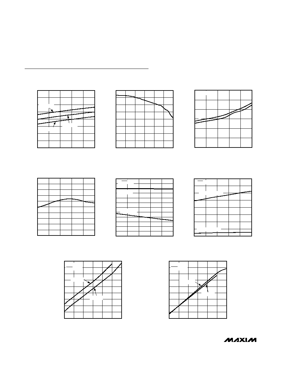
Typical Operating Characteristics
(V
CC
= +3.3V, |V
ID
| = 0.2V, V
CM
= +1.2V, T
A
= +25�C, f
IN
= 1.34GHz, Figure 5.)
SUPPLY CURRENT vs. TEMPERATURE
MAX9394/95 toc01
TEMPERATURE (
�C)
SUPPLY CURRENT (mA)
60
35
-15
10
35
40
45
50
55
60
65
70
30
-40
85
V
CC
= +3.3V
V
CC
= +3.6V
V
CC
= +3.0V
OUTPUT AMPLITUDE vs. FREQUENCY
MAX9394/95 toc02
FREQUENCY (GHz)
OUTPUT AMPLITUDE (mV)
2.0
0.4
1.2
1.6
0.8
50
100
150
200
250
300
350
400
0
0
2.4
OUTPUT RISE/FALL TIME
vs. TEMPERATURE
MAX9394/95 toc03
TEMPERATURE (
�C)
RISE/FALL TIME (ps)
60
35
10
-15
130
140
150
160
170
180
120
-40
85
t
R
t
F
f
IN
= 100MHz
PROPAGATION DELAY
vs. TEMPERATURE
MAX9394/95 toc04
TEMPERATURE (
�C)
PROPAGATION DELAY (ps)
60
35
10
-15
510
520
530
540
550
560
570
580
590
600
500
-40
85
MAX9394 DIFFERENTIAL INPUT CURRENT
vs. TEMPERATURE
MAX9394/95 toc05
TEMPERATURE (
�C)
INPUT CURRENT (
�
A)
60
35
10
-15
-45
-40
-35
-30
-25
-20
-15
-10
-5
0
5
10
-50
-40
85
V
IN_ _
= 3.0V
V
IN_ _
= 0.1V
V
IN_ _
= 0V
MAX9395 DIFFERENTIAL INPUT CURRENT
vs. TEMPERATURE
MAX9394/95 toc06
TEMPERATURE (
�C)
INPUT CURRENT (
�
A)
60
35
-15
10
10
20
30
40
50
60
70
80
0
-40
85
V
IN_ _
= V
CC
V
IN_ _
= (V
CC
- 0.1V)
V
IN_ _
= (V
CC
- 3.0V)
MAX9394
DIFFERENTIAL INPUT CURRENT vs. V
IHD
MAX9394/95 toc07
V
IHD
(V)
INPUT CURRENT (
�
A)
3.0
2.4
0.6
1.2
1.8
-35
-30
-25
-20
-15
-10
-5
0
5
-40
0
3.6
IN_ _ OR
IN_ _ = GND
V
CC
= +3V
V
CC
= +3.6V
MAX9395
DIFFERENTIAL INPUT CURRENT vs. V
ILD
MAX9394/95 toc08
V
ILD
(V)
INPUT CURRENT (
�
A)
3.0
2.4
0.6
1.2
1.8
0
10
20
30
40
50
60
70
80
-10
0
3.6
IN_ _ OR
IN_ _ = V
CC
V
CC
= +3.6V
V
CC
= +3V

MAX9394/MAX9395
2:1 Multiplexers and 1:2 Demultiplexers with
Loopback
_______________________________________________________________________________________
5
Pin Description
PIN
TQFP
QFN
NAME
FUNCTION
1, 2, 3, 30,
31, 32
1, 2, 28
N.C.
No Connection. Not internally connected.
4, 9, 20, 25
3, 8, 18, 23
GND
Ground
5
4
ENB
Channel B Output Enable. Drive ENB high to enable the LVDS outputs for channel B.
An internal 435k
resistor to GND pulls ENB low when unconnected.
6
5
OUTB
Channel B LVDS Noninverting Output. Connect a 100
termination resistor between
OUTB and OUTB at the receiver inputs to ensure proper operation.
7
6
OUTB
Channel B LVDS Inverting Output. Connect a 100
termination resistor between
OUTB and OUTB at the receiver inputs to ensure proper operation.
8, 13, 24, 29
7, 22, 27
V
CC
Power-Supply Input. Bypass each V
CC
to GND with a 0.1�F and 0.01�F ceramic
capacitor. Install both bypass capacitors as close to the device as possible, with the
0.01�F capacitor closest to the device.
10
9
INB0
LVDS/HSTL (MAX9394) or LVPECL/CML (MAX9395) Inverting Input. An internal
128k
pullup resistor to V
CC
pulls the input high when unconnected (MAX9394). An
internal 68k
resistor to GND pulls the input low when unconnected (MAX9395).
11
10
INB0
LVDS/HSTL (MAX9394) or LVPECL/CML (MAX9395) Noninverting Input. An internal
128k
pullup resistor to V
CC
pulls the input high when unconnected (MAX9394). An
internal 68k
resistor to GND pulls the input low when unconnected (MAX9395).
12
11
LB_SELB
Loopback Select for Channel B Output. Connect LB_SELB to GND or leave
unconnected to reproduce the INB_ (INB_) differential inputs at OUTB (OUTB).
Connect LB_SELB to V
CC
to loop back the INA (INA) differential inputs to OUTB
(OUTB). An internal 435k
resistor to GND pulls LB_SELB low when unconnected.
14
12
INB1
LVDS/HSTL (MAX9394) or LVPECL/CML (MAX9395) Inverting Input. An internal
128k
pullup resistor to V
CC
pulls the input high when unconnected (MAX9394). An
internal 68k
resistor to GND pulls the input low when unconnected (MAX9395).
15
13
INB1
LVDS/HSTL (MAX9394) or LVPECL/CML (MAX9395) Noninverting Input. An internal
128k
pullup resistor to V
CC
pulls the input high when unconnected (MAX9394). An
internal 68k
resistor to GND pulls the input low when unconnected (MAX9395).
16
14
BSEL
Channel B Multiplexer Control Input. Selects the differential input to reproduce at the
B channel differential output. Connect BSEL to GND or leave unconnected to select
the INB0 (INB0) set of inputs. Connect BSEL to V
CC
to select the INB1 (INB1) set of
inputs. An internal 435k
resistor to GND pulls BSEL low when unconnected.
17
15
ENA1
Channel A1 Output Enable. Drive ENA1 high to enable the A1 LVDS outputs. An
internal 435k
resistor to GND pulls the ENA1 low when unconnected.
18
16
OUTA1
Channel A1 LVDS Inverting Output. Connect a 100
termination resistor between
OUTA1 and OUTA1 at the receiver inputs to ensure proper operation.
19
17
OUTA1
Channel A1 LVDS Noninverting Output. Connect a 100
termination resistor between
OUTA1 and OUTA1 at the receiver inputs to ensure proper operation.