
General Description
The MAX9450/MAX9451/MAX9452 clock generators
provide high-precision clocks for timing in SONET/SDH
systems or Gigabit Ethernet systems. The MAX9450/
MAX9451/MAX9452 can also provide clocks for the high-
speed and high-resolution ADCs and DACs in 3G base
stations. Additionally, the devices can also be used as a
jitter attenuator for generating high-precision CLK signals.
The MAX9450/MAX9451/MAX9452 feature an integrated
VCXO. This configuration eliminates the use of an exter-
nal VCXO and provides a cost-effective solution for gen-
erating high-precision clocks. The MAX9450/MAX9451/
MAX9452 feature two differential inputs and clock out-
puts. The inputs accept LVPECL, LVDS, differential sig-
nals, and LVCMOS. The input reference clocks range
from 8kHz to 500MHz.
The MAX9450/MAX9451/MAX9452 offer LVPECL, HSTL,
and LVDS outputs, respectively. The output range is up
to 160MHz, depending on the selection of crystal. The
input and output frequency selection is implemented
through the I
2
C or SPITM interface. The MAX9450/
MAX9451/MAX9452 feature clock output jitter less than
0.8ps RMS (in a 12kHz to 20MHz band) and phase-
noise attenuation greater than -130dBc/Hz at 100kHz.
The phase-locked loop (PLL) filter can be set externally,
and the filter bandwidth can vary from 1Hz to 20kHz.
The MAX9450/MAX9451/MAX9452 feature an input
clock monitor with a hitless switch. When a failure is
detected at the selected reference clock, the device
can switch to the other reference clock. The reaction to
the recovery of the failed reference clock can be
revertive or nonrevertive. If both reference clocks fail,
the PLL retains its nominal frequency within a range of
±20ppm at +25∞C.
The MAX9450/MAX9451/MAX9452 operate from 2.4V to
3.6V supply and are available in 32-pin TQFP packages
with exposed pads.
Applications
SONET/SDH Systems
10 Gigabit Network Routers and Switches
3G Cellular Phone Base Stations
General Jitter Attenuation
Features
Integrated VCXO Provides a Cost-Effective
Solution for High-Precision Clocks
8kHz to 500MHz Input Frequency Range
15MHz to 160MHz Output Frequency Range
I
2
C or SPI Programming for the Input and Output
Frequency Selection
PLL Lock Range > ±60ppm
Two Differential Outputs with Three Types of
Signaling: LVPECL, LVDS, or HSTL
Input Clock Monitor with Hitless Switch
Internal Holdover Function within ±20ppm of the
Nominal Frequency
Low Output CLK Jitter: < 0.8ps RMS in the 12kHz
to 20MHz Band
Low Phase Noise > -130dBc at 100kHz, > -140dBc
at 1MHz
MAX9450/MAX9451/MAX9452
High-Precision Clock Generators
with Integrated VCXO
________________________________________________________________ Maxim Integrated Products
1
Ordering Information
19-0547; Rev 2; 9/06
For pricing, delivery, and ordering information, please contact Maxim/Dallas Direct! at
1-888-629-4642, or visit Maxim's website at www.maxim-ic.com.
Note: All devices are specified over the -40∞C to +85∞C
temperature range.
For lead-free packages, contact factory.
*EP = Exposed paddle.
PART
PIN-PACKAGE
OUTPUT
PKG CODE
MAX9450EHJ
32 TQFP-EP*
LVPECL
H32E-6
MAX9451EHJ
32 TQFP-EP*
HSTL
H32E-6
MAX9452EHJ
32 TQFP-EP*
LVDS
H32E-6
MAX9450
MAX9451
MAX9452
TQFP
(5mm x 5mm)
TOP VIEW
EXPOSED PAD
(GND)
24
20
21
22
23
17
18
19
CLK1+
CLK1-
GND
CLK0+
V
DDQ
CLK0-
V
DDQ
OE
2
5
7
6
8
3
4
1
SEL0
IN0-
IN0+
IN1+
V
DD
9
10
11
12
13
14
15
AD1
16
AD0
SDA
SCL
MR
INT
26
27
28
29
30
31
32
RJ
GNDA
LP2
LP1
V
DDA
X2
X1
25
V
DD
SEL1
LOCK
IN1-
GND/CS
CMON
Pin Configuration
SPI is a trademark of Motorola, Inc.
MAX9450/MAX9451/MAX9452
High-Precision Clock Generators
with Integrated VCXO
2
_______________________________________________________________________________________
ABSOLUTE MAXIMUM RATINGS
DC ELECTRICAL CHARACTERISTICS
(V
DDA
= V
DD
= V
DDQ
= 2.4V to 3.6V, and V
DDQ
= 1.4V to 1.6V for MAX9451, T
A
= -40∞C to +85∞C. Typical values at V
DDA
= V
DD
=
V
DDQ
= 3.3V, and V
DDQ
= 1.5V for MAX9451, T
A
= +25∞C, unless otherwise noted.)
Stresses beyond those listed under "Absolute Maximum Ratings" may cause permanent damage to the device. These are stress ratings only, and functional
operation of the device at these or any other conditions beyond those indicated in the operational sections of the specifications is not implied. Exposure to
absolute maximum rating conditions for extended periods may affect device reliability.
V
DD
to GND ...........................................................-0.3V to +4.0V
V
DDA
to GNDA ......................................................-0.3V to +4.0V
All Other Pins to GND ...................................-0.3V to V
DD
+ 0.3V
Short-Circuit Duration (all pins) ..................................Continuous
Continuous Power Dissipation (T
A
= +85∞C)
32-Pin TQFP (derate 27.8mW/∞C above +70∞C)........2222mW
Storage Temperature Range .............................-65∞C to +165∞C
Maximum Junction Temperature .....................................+150∞C
Operating Temperature Range ...........................-40∞C to +85∞C
Lead Temperature (soldering, 10s) .................................+300∞C
ESD Protection
Human Body Model (R
D
= 1.5k
, C
S
= 100pF) ..............±2kV
PARAMETER
SYMBOL
CONDITIONS
MIN
TYP
MAX
UNITS
LVCMOS INPUT (SEL_,
CMON, OE, MR)
Input High Level
V
IH1
2.0
V
DD
V
Input Low Level
V
IL1
0
0.8
V
Input Current
I
IN1
V
IN
= 0V to V
DD
-50
+50
µA
LVCMOS OUTPUT (INT,
LOCK)
Output High Level
V
OH1
I
OH1
= -4mA
V
DD
- 0.4
V
Output Low Level
V
OL1
I
OL1
= 4mA
0.4
V
THREE-LEVEL INPUT (AD0, AD1)
Input High Level
V
IH2
1.8
V
Input Low Level
V
IL2
0.8
V
Input Open Level
V
IO2
Measured at the opened inputs
1.05
1.35
V
Input Current
I
IL2,
I
IH2
V
IL2
= 0V or V
IH2
= V
DD
-15
+15
µA
DIFFERENTIAL INPUTS (IN0, IN1)
Differential Input High Threshold
V
IDH
V
ID
= V
IN+
- V
IN-
50
mV
Differential Input Low Threshold
V
IDL
V
ID
= V
IN+
- V
IN-
-50
mV
Common-Mode Input-Voltage Range
V
COM
V
ID
= V
IN+
-
V
IN-
|V
ID
/ 2|
2.4
- |V
ID
/ 2|
V
Input Current
I
IN+,
I
IN-
-1
+1
µA
MAX9450 OUTPUTS (CLK0, CLK1) (LVPECL)
Output High Voltage
V
OH2
50
load connected to V
DDQ
- 2.0V
V
D D Q
- 1.42
V
D D Q
- 1.00
V
Output Low Voltage
V
OL2
50
load connected to V
DDQ
- 2.0V
V
D D Q
- 2.15
V
D D Q
- 1.70
V
MAX9451 OUTPUTS (CLK0, CLK1) (differential HSTL)
Output High-Level Voltage
V
OH3
W i th 50
l oad r esi stor to G N D , Fi g ur e 1
V
D D Q
- 0.4V
V
D D Q
V
Output Low-Level Voltage
V
OL3
Wi th 50
to GN D and 16m A si nk cur r ent
0.4
V
MAX9452 OUTPUTS (CLK0, CLK1) (LVDS)
Differential Output Voltage
V
OD
With a total 100
load, Figure 1
300
370
450
mV
Change in V
OD
Between
Complementary Output States
V
OD
10
35
mV
MAX9450/MAX9451/MAX9452
High-Precision Clock Generators
with Integrated VCXO
_______________________________________________________________________________________
3
DC ELECTRICAL CHARACTERISTICS (continued)
(V
DDA
= V
DD
= V
DDQ
= 2.4V to 3.6V, and V
DDQ
= 1.4V to 1.6V for MAX9451, T
A
= -40∞C to +85∞C. Typical values at V
DDA
= V
DD
=
V
DDQ
= 3.3V, and V
DDQ
= 1.5V for MAX9451, T
A
= +25∞C, unless otherwise noted.)
PARAMETER
SYMBOL
CONDITIONS
MIN
TYP
MAX
UNITS
Output Offset Voltage
V
OS
1.05
1.2
1.35
V
Change in V
OS
Between
Complementary Output States
V
OS
10
35
mV
Output Short-Circuit Current
I
OS
Two output pins connected to GND
- 7.5
- 15
mA
SERIAL INTERFACE INPUT, OUTPUT (SCL, SDA,
CS)
Input High Level
V
IH
0.7
x V
DD
V
Input Low Level
V
IL
0.3
x V
DD
V
Input Leakage Current
I
IL
-1
+1
µA
Output Low Level
V
OL
3mA sink current
0.4
V
Input Capacitance
C
I
10
pF
POWER CONSUMPTION
MAX9450
55
85
MAX9451
70
94
V
DD
and V
DDA
Supply Current
I
CC1
Output clock
frequency =
155MHz
MAX9452
65
88
mA
MAX9450
55
80
MAX9451
65
80
V
DDQ
Supply Current
I
CC2
Output clock
frequency =
155MHz (MAX9450)
MAX9452
14
25
mA
AC ELECTRICAL CHARACTERISTICS
(V
DDA
= V
DD
= V
DDQ
= 2.4V to 3.6V, and V
DDQ
= 1.4V to 1.6V for MAX9451, T
A
= -40∞C to +85∞C. |V
ID
| = 200mV, V
COM
= |V
ID
/ 2| to
2.4 - |V
ID
/ 2|. Typical values at V
DDA
= V
DD
= V
DDQ
= 3.3V and V
DDQ
= 1.5V for MAX9451, T
A
= +25∞C. C
L
= 10pF, clock output =
155.5MHz and clock input = 19.44MHz, unless otherwise noted.) (Note 1)
PARAMETER
SYMBOL
CONDITIONS
MIN
TYP
MAX
UNITS
CLK OUTPUTS (CLK0, CLK1)
Reference Input Frequency
f
IN
Measured at IN0 or IN1
0.008
500
MHz
Output Frequency
f
OUT
Measured at CLK0 or CLK1
15
160
MHz
VCXO Pulling Range
C
L
= 8pF (Note 2)
±60
ppm
Skew between CLK0 and CLK1
(MAX9450 and MAX9452)
50
90
Output-to-Output Skew
t
SKO
Skew between C LK0 and C LK1 (M AX9451)
55
106
ps
Rise Time
t
R
20% to 80% of output swing
0.4
0.590
ns
Fall Time
t
F
80% to 20% of output swing
0.4
0.590
ns
Duty Cycle
43
56
%
Period Jitter (RMS)
T
J
Measured at the band 12kHz to 20MHz
0.8
ps
1kHz offset
-70
10kHz offset
-110
100kHz offset
-130
Phase Noise
1MHz offset
-140
dBc

Note 1: All timing AC electrical characteristics and timing specifications are guaranteed by design and not production tested.
Note 2: The VCXO tracks the input clock frequency by ±60ppm.
Note 3: A master device must provide a hold time of at least 300ns for the SDA signal to bridge the undefined regions of SCL's
falling edge.
Note 4: C
B
= total capacitance of one bus line in pF. Tested with C
B
= 400pF.
Note 5: Input filters on SDA and SCL suppress noise spikes less than 50ns.
PARAMETER
SYMBOL
CONDITIONS
MIN
TYP
MAX
UNITS
Serial-Clock Frequency
f
SCL
2
MHz
CS Fall to CLK Rise Setup Time
t
CSS
12.5
ns
DIN Setup Time
t
DS
12.5
ns
DIN Hold Time
t
DH
0
ns
CLK High to
CS High
t
CSH
0
ns
CS Pulse-High Time
t
CSW
20
ns
SERIAL SPI INTERFACE TIMING CHARACTERISTICS
(VDD = 2.4V to 3.6V, TA = -40∞C to +85∞C. See Figure 7 for the timing parameters definition.)
MAX9450/MAX9451/MAX9452
High-Precision Clock Generators
with Integrated VCXO
4
_______________________________________________________________________________________
PARAMETER
SYMBOL
CONDITIONS
MIN
TYP
MAX
UNITS
Serial Clock
f
SCL
400
kHz
Bus Free Time Between STOP and
START Conditions
t
BUF
1.3
µs
Rep eated H ol d Ti m e S TART C ond i ti on
t
HD,STA
0.6
µs
Rep eated S TART C ond i ti on S etup Ti m e
t
SU,STA
0.6
µs
STOP Condition Setup Time
t
SU,STO
0.6
µs
Data Hold Time
t
HD,DAT
(Note 3)
100
ns
Data Setup Time
t
SU,DAT
100
ns
SCL Clock-Low Period
t
LOW
1.3
µs
SCL Clock-High Period
t
HIGH
0.7
µs
Maximum Receive SCL/SDA Rise Time
t
R
300
ns
Minimum Receive SCL/SDA Rise Time
t
R
(Note 4)
20
+ 0.1 x C
b
ns
Maximum Receive SCL/SDA Fall Time
t
F
300
ns
Minimum Receive SCL/SDA Fall Time
t
F
(Note 4)
20
+ 0.1 x C
b
ns
Fall Time of SDA, Transmitting
t
F,TX
(Note 4)
20
+ 0.1C
b
250
ns
Pulse Width of Suppressed Spike
t
SP
(Note 5)
0
50
ns
Capacitive Load for Each Bus Line
C
B
(Note 4)
400
pF
SERIAL I
2
C-COMPATIBLE INTERFACE TIMING CHARACTERISTICS
(VDD = 2.4V to 3.6V, TA = -40∞C to +85∞C. See Figure 4 for the timing parameters definition.)
MAX9450/MAX9451/MAX9452
High-Precision Clock Generators
with Integrated VCXO
_______________________________________________________________________________________
5
V
DD
AND V
DDA
SUPPLY CURRENT
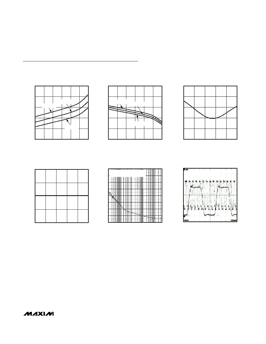
vs. VOLTAGE (MAX9450)
MAX9450 toc01
VOLTAGE (V)
I
DD
+ I
DDA
(mA)
3.2
3.0
2.8
2.6
48
56
64
72
80
40
2.4
3.6
3.4
T
A
= -40
∞C
T
A
= +25
∞C
T
A
= +85
∞C
V
DDQ
SUPPLY CURRENT
vs. VOLTAGE (MAX9450)
MAX9450 toc02
VOLTAGE (V)
I
DDQ
(mA)
3.2
3.0
2.8
2.6
48
56
64
72
80
40
2.4
3.6
3.4
T
A
= -40
∞C
T
A
= +25
∞C
T
A
= +85
∞C
OUTPUT FREQUENCY CHANGE
vs. TEMPERATURE
MAX9450 toc04
TEMPERATURE (
∞C)
OUTPUT FREQUENCY CHANGE (ppm)
60
35
-15
10
-20
0
20
40
-40
-40
85
PHASE NOISE
vs. FREQUENCY
MAX9450 toc05
PHASE NOISE (dBc)
100k
FREQUENCY (Hz)
1M
10M
10k
1k
0
-20
-40
-60
-80
-100
-120
-140
-160
INPUT REFERENCE = 38.88 MHz
OUTPUT CLOCK = 155.52 MHz
OUTPUT RMS JITTER
vs. TEMPERATURE
MAX9450 toc03
TEMPERATURE (
∞C)
RMS JITTER (ps)
60
35
10
-15
2
4
6
8
10
0
-40
85
OUTPUT CLOCK SYNCHRONIZED
TO INPUT REFERENCE
MAX9450 toc06
153.13mV/div
100mV/div
10ns/div
INPUT REFERENCE = 19.44MHz
OUTPUT CLOCK = 155.52 MHz
Typical Operating Characteristics
(V
DD
= V
DDA
= V
DDQ
= 3.3V. T
A
= +25∞C, unless otherwise noted.)