General Description
The MAX9480/MAX9481/MAX9482 low-power, low-dis-
tortion, class-G, high-current asymmetric digital sub-
scriber line (ADSL) drivers offer Rail-to-Rail
Æ
output and
are ideal for ADSL in central-office applications.
Operating from ±5V and ±2.5V supplies, the drivers
incorporate two high-speed current-feedback preampli-
fiers driving two fixed-gain class-G buffers. The buffers
can deliver 20.4dBm average line power with a signal
crest factor of 5.3, and are designed to be directly DC or
AC bridged across a 1:2.5 transformer.
The MAX9480/MAX9481/MAX9482 employ an active line
termination scheme for incoming signals that eliminates
the need for back-match resistors, reducing line-card
power consumption at full rate to less than half of that
required by conventional class-AB line-driver circuits.
The MAX9480 includes a hybrid network and two low-
noise, fixed-gain-of-4.6V/V receive amplifiers. The part is
designed to recover the receive signal to the same level
as that of a conventional line interface circuit that incor-
porates a 1:2 transformer and standard back-matched
hybrid, without degrading signal-to-noise ratio (SNR) or
line-impedance sensitivity. The MAX9481 provides only
the preamplifiers and buffers without the hybrid or
receivers. The MAX9482 provides preamplifiers, buffers,
and uncommitted receive amplifiers. All devices have a
low-output-impedance shutdown function for saving
power when not transmitting.
At full-rate 20.4dBm discrete multitone data transmission
(DMT), the total dynamic power dissipation is only
680mW (MAX9480/MAX9482) or 655mW (MAX9481).
The MAX9480/MAX9481 are available in a 20-pin TSSOP
package and the MAX9482 is available in 28-pin TSSOP
and 32-pin QFN packages. All devices operate over the
extended -40∞C to +85∞C temperature range.
Applications
Full-Rate ADSL
HDSL
Central Office
DSLAM
Features
o Dissipate Only 655mW While Driving 20.4dBm
ADSL Full-Rate DMT-Modulated Signal
o Operate with ±5.0V and ±2.5V Power Supplies
o Complete ADSL Central-Office Line Interface
(MAX9480/MAX9482)
Two Preamplifiers plus Class-G Rail-to-Rail
Buffers
Active Line Termination plus Integrated Hybrid
(MAX9480)
Low-Noise Uncommitted Receive Amplifiers
(MAX9482)
Fixed-Gain Receive Amplifiers (MAX9480)
Low-Output-Impedance Shutdown Mode
o Preamplifiers, Buffers, and Active Line
Termination Functions (MAX9481)
o High-Output-Drive Capability
15V
P-P
Differential Output Voltage Swing at
R
L
= 16
500mA Output-Drive
o Low Distortion: -71dBc Highest Harmonic at 1MHz
and 14V
P-P
o High Speed: 250V/µs Slew Rate, 80MHz -3dB
Bandwidth (G = -3)
o Thermal Shutdown
o Exposed Pads Improve Thermal Performance
MAX9480/MAX9481/MAX9482
Low-Power, Low-Distortion, Central-Office
ADSL Drivers and Integrated Drivers/Receivers
________________________________________________________________ Maxim Integrated Products
1
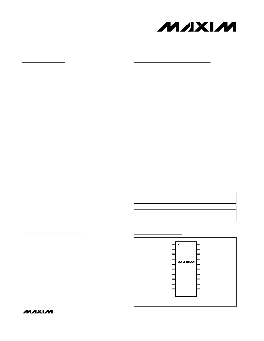
20
19
18
17
16
15
14
13
1
2
3
4
5
6
7
8
V
LM
V
LP
V
CC
OUT1
RXP
IN1+
IN1-
POUT1
TOP VIEW
V
EE
V
EE
OUT2
V
CC
IN2+
RXM
SHDN
DGND
12
11
9
10
V
LP
V
LM
POUT2
IN2-
MAX9480
TSSOP
Pin Configurations
Ordering Information
19-2539; Rev 1; 1/03
For pricing, delivery, and ordering information, please contact Maxim/Dallas Direct! at
1-888-629-4642, or visit Maxim's website at www.maxim-ic.com.
PART
TEMP RANGE
PIN-PACKAGE
MAX9480CUP
-40
∞C to +85∞C
20 TSSOP-EP**
MAX9481CUP
-40
∞C to +85∞C
20 TSSOP-EP
MAX9482CUI
-40
∞C to +85∞C
28 TSSOP-EP
MAX9482CGJ*
-40
∞C to +85∞C
32 QFN
Typical Operating Circuits appear at end of data sheet.
Rail-to-Rail is a registered trademark of Nippon Motorola, Ltd.
Pin Configurations continued at end of data sheet.
*Future product--contact factory for availability.
**EP = Exposed pad.

MAX9480/MAX9481/MAX9482
Low-Power, Low-Distortion, Central-Office
ADSL Drivers and Integrated Drivers/Receivers
2
_______________________________________________________________________________________
ABSOLUTE MAXIMUM RATINGS
Stresses beyond those listed under "Absolute Maximum Ratings" may cause permanent damage to the device. These are stress ratings only, and functional
operation of the device at these or any other conditions beyond those indicated in the operational sections of the specifications is not implied. Exposure to
absolute maximum rating conditions for extended periods may affect device reliability.
V
CC
to V
EE
...........................................................................+12V
V
LP
to V
LM
............................................................................+12V
V
CC
or V
LP
to DGND ................................................-0.3V to +6V
V
CC
to V
LP
................................................................-0.3V to +6V
V
EE
or V
LM
to DGND ................................................-6V to +0.3V
V
EE
to V
LM
................................................................-6V to +0.3V
Current into V
LP
or V
LM
..................................................±250mA
IN1+, IN1-, IN2+, IN2-......................(V
CC
+ 0.3V) to (V
EE
- 0.3V)
SHDN ...............................................(V
CC
+ 0.3V) to (V
EE
- 0.3V)
BOUT1/BOUT2 Output Short-Circuit Duration to
V
CC
/V
EE
/V
LP
/V
LM
....................................................Momentary
BOUT1/BOUT2 Output Current...........................................20mA
OUT1/OUT2 Output Short-Circuit Duration to
V
CC
/V
EE
/V
LP
/V
LM
....................................................Momentary
OUT1/OUT2 Output Current ....................................................1A
OUT1 to OUT2 Short-Circuit Duration ........................Continuous
POUT1/POUT2 Output Short-Circuit Duration to
V
CC
/V
EE
/V
LP
/V
LM
................................................................10s
POUT1/POUT2 Output Current .........................................100mA
RXP/RXM Output Short-Circuit Duration to
V
CC
/V
EE
/V
LP
/V
LM
................................................................10s
RXP/RXM Output Current..................................................100mA
Continuous Power Dissipation (T
A
= +70∞C)
20-Pin TSSOP with Pad Connected to V
EE
(derate 21.7mW/∞C above +70∞C) ..............................1739mW
20-Pin TSSOP with Floating Pad
(derate 11.0mW/∞C above +70∞C) ................................879mW
28-Pin TSSOP with Pad Connected to V
EE
(derate 23.8mW/∞C above +70∞C) ..............................1905mW
28-Pin TSSOP with Floating Pad
(derate 12.8mW/∞C above +70∞C) ..............................1026mW
32-Pin QFN (derate 23.3mW/∞C above +70∞C) .........1860mW*
Operating Temperature Range
(T
MIN
, T
MAX
) .....................................................-40∞C to +85∞C
Junction Temperature ......................................................+150∞C
Storage Temperature Range .............................-65∞C to +150∞C
Lead Temperature (soldering, 10s) .................................+300∞C
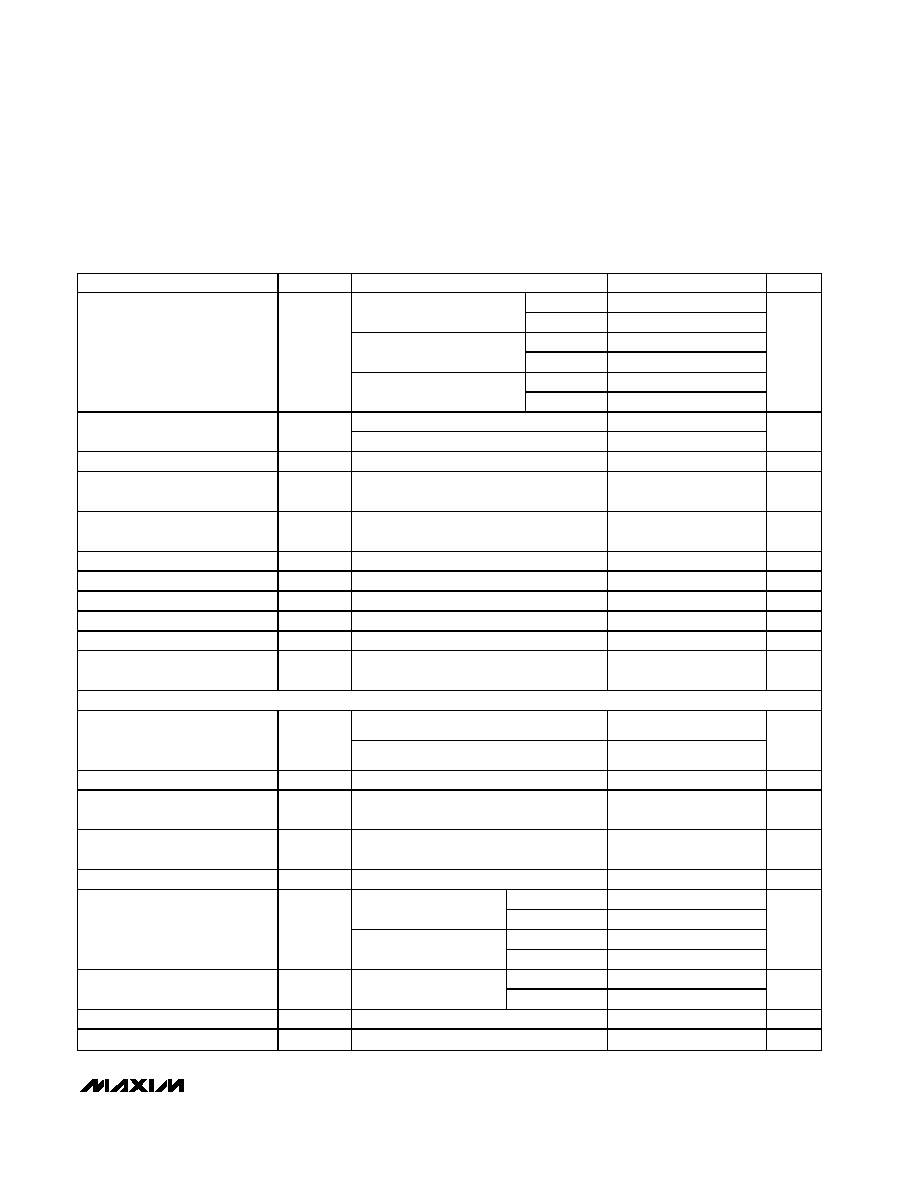
ELECTRICAL CHARACTERISTICS
(V
CC
= +5V, V
EE
= -5V, V
LP
= +2.5V, V
LM
= -2.5V, DGND = 0, R
L
= 16
is connected from OUT1 to OUT2, SHDN = 0, T
A
= T
MIN
to
T
MAX
, unless otherwise noted. Typical values specified at T
A
= +25∞C. Preamp configured for A
V
= +1 with 1k
from POUT_ to IN_-.)
(Note 1)
PARAMETER
SYMBOL
CONDITIONS
MIN
TYP
MAX
UNITS
MAX9480/
MAX9482
680
Dynamic Power Dissipation
P
DISS
V
OUT(DIFF)
= 1.327V
RMS
,
crest factor = 5.3
MAX9481
655
mW
MAX9480/
MAX9482
790
Dynamic Power Consumption
P
CONS
V
OUT(DIFF)
= 1.327V
RMS
,
crest factor = 5.3
MAX9481
765
mW
V
CC
(Note 2)
4.75
5.00
5.25
V
EE
(Note 2)
-4.75
-5.00
-5.25
V
LP
(Note 2)
2.25
2.50
2.75
Supply Voltage Range
V
LM
(Note 2)
-2.25
-2.50
-2.75
V
V
CC
, V
EE
21.5
35.0
MAX9480, R
L
=
V
LP
, V
LM
22.0
40.0
V
CC
, V
EE
20.0
34.0
MAX9481, R
L
=
V
LP
, V
LM
21.0
39.0
V
CC
, V
EE
21.5
35.0
Quiescent Supply Current
(Including Preamps)
I
CC
, I
EE
,
I
LP
, I
LM
MAX9482, R
L
=
V
LP
, V
LM
22.0
40.0
mA
*Refer to Application Note HFAN-08-1.
MAX9480/MAX9481/MAX9482
Low-Power, Low-Distortion, Central-Office
ADSL Drivers and Integrated Drivers/Receivers
_______________________________________________________________________________________
3
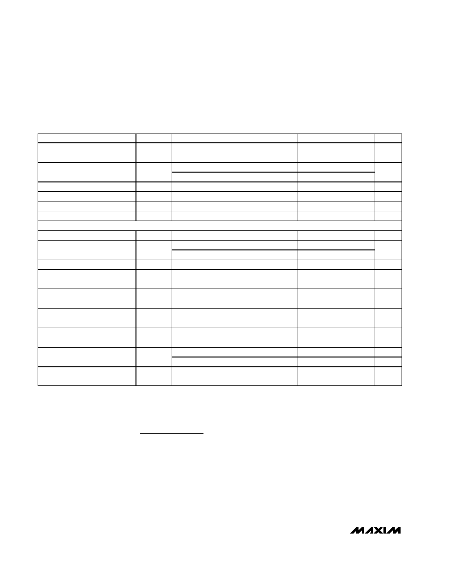
ELECTRICAL CHARACTERISTICS (continued)
(V
CC
= +5V, V
EE
= -5V, V
LP
= +2.5V, V
LM
= -2.5V, DGND = 0, R
L
= 16
is connected from OUT1 to OUT2, SHDN = 0, T
A
= T
MIN
to
T
MAX
, unless otherwise noted. Typical values specified at T
A
= +25∞C. Preamp configured for A
V
= +1 with 1k
from POUT_ to IN_-.)
(Note 1)
PARAMETER
SYMBOL
CONDITIONS
MIN
TYP
MAX
UNITS
V
CC
, V
EE
2.1
6.0
MAX9480, R
L
=
V
LP
, V
LM
1.5
5.0
V
CC
, V
EE
0.6
1.2
MAX9481, R
L
=
V
LP
, V
LM
0.05
0.1
V
CC
, V
EE
2.1
6.0
Shutdown Supply Current
I
SD
MAX9482, R
L
=
V
LP
, V
LM
1.5
5.0
mA
V
CC
- V
EE
= ±4.75V to ±5.25V
50
76
Transmit Path Power-Supply
Rejection Ratio (Single Ended)
PSRR
V
LP
- V
LM
= ±2.25V to ±2.75V
50
81
dB
Common-Mode Rejection
CMR
-200mV
V
CM
+200mV
46
dB
Hybrid Rejection Ratio
(MAX9480 Only)
HRR
V
OUT(DIFF)
= ±1.2V
35
dB
Driver-to-Receiver Crosstalk
(MAX9482 Only)
X
TALK
f = 100kHz
-69
dB
SHDN Logic Low
V
IL
0.8
V
SHDN Logic High
V
IH
2.0
V
SHDN Input Current
I
IH
, I
IL
SHDN = 0 or SHDN = V
CC
±5.0
µA
Shutdown Delay Time
t
SHDN
4.8
µs
Shutdown Enable Time
t
ENABLE
4
µs
Intermodulation Distortion
I
MD
f1 = 1MHz, f2 = 900kHz, Typical Operating
Circuit, V
OUT(DIFF)
= 2.0V
P-P
-66
dB
DRIVER
DMT modulation (crest factor, Cr = 5.33)
21.4
Maximum RMS Output Power
(Typical Operating Circuit)
(Note 3)
P
OUT
CAP modulation (crest factor, Cr = 4.00)
24.3
dBmW
Closed-Loop Gain
G
V
OUT(DIFF)
= 1.2V
P-P
-2.7
-3
-3.3
V/V
Second Harmonic Distortion
f = 1MHz, V
OUT(DIFF)
= 14V
P-P
,
Typical Operating Circuit (Note 4)
-71
dB
Third Harmonic Distortion
f = 1MHz, V
OUT(DIFF)
= 14V
P-P
, Typical
Operating Circuit (Note 4)
-74
dB
Differential Output Voltage Swing
V
OUT(DIFF)
Typical Operating Circuit (Note 4)
15.0
V
P-P
V
CC
- V
OH
0.5
R
L
= 100
|V
EE
- V
OL
|
0.5
V
CC
- V
OH
1.27
OUT_ Voltage Swing
(per Amplifier) (Note 4)
V
OH
, V
OL
R
L
= 16
|V
EE
- V
OL
|
1.21
V
V
CC
- V
BOH
0.45
BOUT_ Voltage Swing
(per Amplifier) (Note 4)
V
BOH
,
V
BOL
|V
EE
- V
BOL
|
0.42
V
Peak Output Current
I
OUT
500
mA
Differential Output Offset Voltage
V
OS(DIFF)
IN1+ = IN2+ = 0
±5
mV
MAX9480/MAX9481/MAX9482
Low-Power, Low-Distortion, Central-Office
ADSL Drivers and Integrated Drivers/Receivers
4
_______________________________________________________________________________________
ELECTRICAL CHARACTERISTICS (continued)
(V
CC
= +5V, V
EE
= -5V, V
LP
= +2.5V, V
LM
= -2.5V, DGND = 0, R
L
= 16
is connected from OUT1 to OUT2, SHDN = 0, T
A
= T
MIN
to
T
MAX
, unless otherwise noted. Typical values specified at T
A
= +25∞C. Preamp configured for A
V
= +1 with 1k
from POUT_ to IN_-.)
(Note 1)
PARAMETER
SYMBOL
CONDITIONS
MIN
TYP
MAX
UNITS
Differential Output Offset-Voltage
Drift
V
OS(DRIFT)
±12
µV/
∞C
-200mV
V
OUT
+200mV
6
8
10
Output Resistance (per Amplifier)
R
OUT
SHDN = V
CC
8
-3dB Bandwidth
BW
80
MHz
Slew Rate
SR
V
OUT(DIFF)
= 14V
P-P
step
250
V/µs
Output Noise PSD
P
N
f = 100kHz to 1.1MHz, referred to 100
line
-127
dBm/Hz
Capacitive Load Stability
No sustained oscillations
1000
pF
PREAMPS AND RECEIVERS (Note 5)
Open-Loop Transimpedance
Z
OL
-2V
P
OUT
+2V
300
k
V
CC
- V
EE
= ±4.75V to ±5.25V
50
87
Power-Supply Rejection Ratio
PSRR
V
LP
- V
LM
= ±2.25V to ±2.75V
50
100
dB
Input Offset Voltage
V
OS
±2
±10
mV
IN1+, IN2+, RXIN1+, RXIN2+
Bias Current
I
B+
±1
±20
µA
IN1+, IN2+, RXIN1+, RXIN2+
Bias Current Matching
I
OS+
±0.7
µA
IN1-, IN2-, RXIN1-, RXIN2-
Bias Current
I
B-
±2.6
±20
µA
IN1-, IN2-, RXIN1-, RXIN2-
Bias Current Matching
I
OS-
±1.2
µA
IN1+, IN2+, RXIN1+, RXIN2+
1.1
M
Input Resistance
R
IN
IN1-, IN2-, RXIN1-, RXIN2-
200
Input Capacitance
C
IN
IN1+, IN2+, IN1-, IN2-, RXIN1+, RXIN2+,
RXIN1-, RXIN2-
2
pF
Note 1: All devices are 100% production tested at T
A
= +25∞C. Specifications over temperature limits are guaranteed by design.
Note 2: Guaranteed by the PSRR test.
Note 3: Implied by worst-case output voltage swing (V
OUT(DIFF)
), crest factor (Cr), and load impedance (R
L
):
Note 4: Device may exceed absolute maximum ratings for power dissipation if unit is subjected to full-scale sinusoids for long
periods. See the Applications Information section.
Note 5: Receiver specifications guaranteed for MAX9482 only.
P
V
Cr
R
dBmW
DRIVER
OUT DIFF
L
=
◊
◊
10
250
10
2
2
log
(
)

MAX9480/MAX9481/MAX9482
Low-Power, Low-Distortion, Central-Office
ADSL Drivers and Integrated Drivers/Receivers
_______________________________________________________________________________________
5
Typical Operating Characteristics
(V
CC
= +5V, V
EE
= -5V, V
LP
= +2.5V, V
LM
= -2.5V, DGND = 0, RXIN1+ = RXIN2+ = 0, IN1+ = IN2+ = 0, R
L
= 16
is connected from
OUT1 to OUT2, SHDN = 0, T
A
= +25∞C, unless otherwise noted. Preamp configured for A
V
= +1 with 1k
from RXOUT_- to RXIN_-.
Receiver configured for A
V
= +1 with 1k
from POUT_ to IN_-.)
SUPPLY CURRENT vs. OUTPUT VOLTAGE
MAX9480 toc01
V
OUT
P-P
(V)
SUPPLY CURRENT (mA)
9
8
7
6
5
4
3
2
1
100
200
300
400
500
600
0
0
10
=
±5V SUPPLY
=
±2.5V SUPPLY
INPUT = DC
f
INPUT
= 1MHz
I
DC
I
AVG
I
AVG
f
INPUT
= 100kHz
SUPPLY CURRENT vs. TEMPERATURE
MAX9480 toc02
TEMPERATURE (
∞C)
SUPPLY CURRENT (mA)
60
35
10
-15
14
18
22
26
30
10
-40
85
2.5V SUPPLY
5V SUPPLY
MAX9481
TRANSMIT PATH
FREQUENCY RESPONSE
MAX9480 toc04
FREQUENCY (MHz)
GAIN (dB)
10
1
0.1
-60
-40
-20
0
20
40
60
80
-80
PHASE (DEGREES)
-280
-260
-240
-220
-200
-180
-160
-140
-300
0.01
100
= GAIN
= PHASE
OVERALL GAIN = -9V/V
PREAMP GAIN = +3V/V
OVERALL GAIN = -3V/V
PREAMP GAIN = +1V/V
DRIVER HARMONIC DISTORTION
vs. FREQUENCY
MAX9480 toc05
FREQUENCY (MHz)
HARMONIC DISTORTION (dBc)
1
0.1
-80
-60
-40
-20
0
-100
0.01
10
V
OUT
P-P
= 2.0V
2ND HARMONIC
3RD HARMONIC
2ND HARMONIC
2ND HARMONIC
SHUTDOWN CURRENT vs. TEMPERATURE
MAX9480 toc03
TEMPERATURE (
∞C)
SHUTDOWN CURRENT (mA)
60
35
10
-15
0.6
1.2
1.8
2.4
3.0
0
-40
85
2.5V SUPPLY
5V SUPPLY
MAX9481
DRIVER HARMONIC DISTORTION
vs. OUTPUT VOLTAGE
MAX9480 toc06
V
OUT
(DIFF) (V
P-P
)
HARMONIC DISTORTION (dBc)
16
14
10
12
6
8
4
-90
-80
-70
-60
-50
-40
-30
-20
-10
0
-100
2
18
2ND HARMONIC
3RD HARMONIC
2ND HARMONIC
2ND HARMONIC
f = 1MHz
SUPPLY CROSSOVER REGION
RECEIVER AMPLIFIER
FREQUENCY RESPONSE
MAX9480 toc07
FREQUENCY (MHz)
GAIN (dB)
100
10
1
0.1
-30
-20
-10
0
10
20
30
-40
PHASE (DEGREES)
-90
-45
0
45
90
135
-135
0.01
1000
A: GAIN = 10V/V
B: GAIN = 5V/V
C: GAIN = 1V/V
= GAIN
= PHASE
A
B
C
A
B
C