
General Description
The MAX9502 small, low-power video amplifier with
integrated reconstruction filter operates from a supply
voltage as low as 2.5V. The small size and the low mini-
mum supply voltage make the MAX9502 ideal for
portable applications such as mobile phones, digital
still cameras, and camcorders.
The MAX9502 DC-couples the input and the output,
resulting in a very small solution. The MAX9502 input can
be directly connected to the output of a video digital-to-
analog converter (DAC). The reconstruction filter is imple-
mented as a 4th-order Chebyshev with a minimum
passband of 5.5MHz, 3dB attenuation at 8MHz, and
55dB attenuation at 27MHz.
The output amplifier provides a closed-loop gain of
+6dB (MAX9502G) or +12dB (MAX9502M), and can
drive a 2V
P-P
video signal into a 150
load to ground.
The output signal is level-shifted so the sync tip is
110mV (typ) above ground.
The MAX9502 operates from a 2.5V to 3.6V single supply
and consumes only 5.3mA quiescent supply current.
An active-low shutdown mode reduces the supply
current to 0.01µA.
The MAX9502 is available in tiny 6-pin µDFN (1mm x
1.5mm x 0.8mm) and 5-pin SC70 packages. The
device is specified over the -40∞C to +85∞C extended
temperature range.
Applications
Mobile Phones/Smartphones
Digital Still Cameras
Portable Media Players
Camcorders
Features
Tiny 6-Pin µDFN (1mm x 1.5mm x 0.8mm) and
5-Pin SC70 Packages
DC-Coupled Input and Output Save Board Space
4-Pole Chebyshev Filter
5.5MHz Passband
55dB Attenuation at 27MHz
0.01µA Low-Current Shutdown Mode
2.5V to 3.6V Single-Supply Operation
Video Amplifier with Fixed Gains of +6dB
(MAX9502G) or +12dB (MAX9502M)
MAX9502
2.5V Video Amplifier with Reconstruction Filter
________________________________________________________________ Maxim Integrated Products
1
Pin Configurations
Ordering Information
19-3674; Rev 0; 5/05
For pricing, delivery, and ordering information, please contact Maxim/Dallas Direct! at
1-888-629-4642, or visit Maxim's website at www.maxim-ic.com.
*All devices are specified over the -40∞C to +85∞C operating
temperature range.
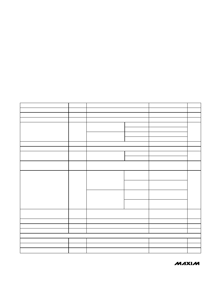
PART*
PIN-PACKAGE
GAIN
(dB)
TOP
MARK
MAX9502GEXK-T
5 SC70-5
+6
ARV
MAX9502GELT-T
6 µDFN-6 (L611-1)
+6
AU
MAX9502MEXK-T
5 SC70-5
+12
ARW
MAX9502MELT-T
6 µDFN-6 (L611-1)
+12
AV
Typical Operating Circuit appears at end of data sheet.
TOP VIEW
SC70
GND
V
CC
SHDN
1
5
OUT
IN
MAX9502
2
3
4
GND
V
CC
1
6
OUT
5
N.C.
IN
MAX9502
µDFN
2
3
4
SHDN
Other Portable Video Amplifiers
PRODUCT
FEATURES
MAX9503
DirectDriveTM, LPF, DC-coupled
input/output, 50dB at 27MHz, TQFN
MAX9505
DirectDrive, LPF, DC-coupled input/output,
50dB at 27MHz analog switch, TQFN
MAX4090
Video amplifier, input clamp, µDFN,
SOT23, SC70
MAX9504
Video amplifier, 2 DC-coupled loads,
optional DC offset bias, µDFN, SOT23
MAX9502
2.5V Video Amplifier with Reconstruction Filter
2
_______________________________________________________________________________________
ABSOLUTE MAXIMUM RATINGS
DC ELECTRICAL CHARACTERISTICS
(V
CC
= SHDN = 3.0V, GND = 0V, no load, T
A
= T
MIN
to T
MAX
, unless otherwise noted. Typical values are at T
A
= +25∞C, unless otherwise
noted.) (Note 1)
Stresses beyond those listed under "Absolute Maximum Ratings" may cause permanent damage to the device. These are stress ratings only, and functional
operation of the device at these or any other conditions beyond those indicated in the operational sections of the specifications is not implied. Exposure to
absolute maximum rating conditions for extended periods may affect device reliability.
V
CC
to GND ..............................................................-0.3V to +4V
SHDN, IN, OUT to GND..............................-0.3V to (V
CC
+ 0.3V)
OUT Short-Circuit Duration to V
CC
, GND..................Continuous
Continuous Power Dissipation (T
A
= +70∞C)
5-Pin SC70 (derate 3.1mW/∞C above +70∞C)........... .247mW
6-Pin µDFN (derate 2.1mW/∞C above +70∞C)............168mW
Operating Temperature Range ...........................-40∞C to +85∞C
Junction Temperature ......................................................+150∞C
Storage Temperature Range .............................-65∞C to +150∞C
Lead Temperature (soldering, 10s) .................................+300∞C
PARAMETER
SYMBOL
CONDITIONS
MIN
TYP
MAX
UNITS
Supply Voltage Range
V
CC
Guaranteed by PSRR
2.5
3.6
V
Quiescent Supply Current
I
CC
V
IN
= 0V, 2.5V
V
CC
3.6V, SHDN = V
CC
5.3
9
mA
Shutdown Supply Current
I
SHDN
V
SHDN
= 0V
0.01
1
µA
V
CC
= 2.5V
0
1.05
Guaranteed by DC
voltage gain (MAX9502G)
V
CC
= 3.0V
0
1.2
V
CC
= 2.5V
0
0.525
Input Voltage Range
V
IN
Guaranteed by DC
voltage gain (MAX9502M)
V
CC
= 3.0V
0
0.6
V
Input Current
I
IN
V
IN
= 0V
3.5
10
µA
Input Resistance
R
IN
V
IN
/
I
IN
17
M
MAX9502G
5.5
6
6.5
DC Voltage Gain (Note 2)
A
V
R
L
= 150
to GND,
V
CC
= 2.5V to 3V
MAX9502M
11.5
12
12.5
dB
Output Sync-Tip Level
V
STIP
Measured at OUT, V
IN
= 0V,
R
L
= 150
to GND
110
230
mV
V
CC
= 2.5V,
0
V
IN
1.05V
1.97
2.1
2.23
MAX9502G,
R
L
= 150
to GND
V
CC
= 3.0V,
0
V
IN
1.2V
2.26
2.4
2.54
V
CC
= 2.5V,
0
V
IN
0.525V
1.97
2.1
2.23
Output Voltage Swing
V
OUT
MAX9502M,
R
L
= 150
to GND
V
CC
= 3.0V,
0
V
IN
0.6V
2.26
2.4
2.54
V
P-P
Output Short-Circuit Current
Threshold
I
SC
Sourcing (Note 3)
95
mA
Output Resistance
R
OUT
0.15
Shutdown Output Impedance
R
OUT(OFF)
V
SHDN
= 0V
4
k
DC Power-Supply Rejection Ratio
PSRR
DC
V
IN
= 0V, 2.5V
V
CC
3.6V
50
90
dB
LOGIC INPUTS (SHDN)
Logic-Low Level
V
IL
0.8
V
Logic-High Level
V
IH
2.0
V
Logic Input Current
I
IL
SHDN = GND and V
CC
1
µA

MAX9502
2.5V Video Amplifier with Reconstruction Filter
_______________________________________________________________________________________
3
PARAMETER
SYMBOL
CONDITIONS
MIN
TYP
MAX
UNITS
Passband Flatness
V
OUT
= 2V
P-P
, f = 100kHz to 5.5MHz,
flatness is referred to 100kHz
-1
+1
dB
f = 8MHz
3
Attenuation
f
dt
V
OUT
= 2V
P-P
, attenuation is
referred to 100kHz
f = 27MHz
35
55
dB
Power-Supply Rejection Ratio
PSRR
f = 100kHz
56
dB
Output Impedance
Z
OUT
V
OUT
= 1.5V DC; f = 5MHz
2.5
MAX9502G
0.4
Differential Gain Error
DG
NTSC, V
OUT
= 2V
P-P
MAX9502M
0.4
%
MAX9502G
0.4
Differential Phase Error
DP
NTSC, V
OUT
= 2V
P-P
MAX9502M
0.4
degrees
2T Pulse-to-Bar K Rating
2T = 250ns; bar time is 18µs; the beginning
2.5% and the ending 2.5% of the bar time
are ignored
0.2
K%
2T Pulse Response
2T = 250ns
0.3
K%
2T Bar Response
2T = 250ns; bar time is 18µs; the beginning
2.5% and the ending 2.5% of the bar time
are ignored
0.4
K%
Nonlinearity
5-step staircase
0.4
%
Line Time Distortion
0
%
Field Time Distortion
0
%
MAX9502G
30
Group-Delay Variation
(d/d)
f = 100kHz to 5.5MHz
MAX9502M
30
ns
MAX9502G
68
Peak Signal to RMS Noise
SNR
V
OUT
= 2V
P-P
, 100kHz to
5MHz
MAX9502M
65
dB
MAX9502G
(V
IN
= 1V)
800
Enable Time
t
ON
V
SHDN
= 3V, V
OUT
settled to
within 1% of the final voltage
MAX9502M
(V
IN
= 0.5V)
800
ns
MAX9502G
(V
IN
= 1V)
220
Disable Time
t
OFF
V
SHDN
= 0V, V
OUT
settled to
below 1% of the output
voltage
MAX9502M
(V
IN
= 0.5V)
175
ns
Note 1: All devices are 100% production tested at T
A
= +25∞C. Specifications over temperature limits are guaranteed by design.
Note 2: DC voltage gain (A
V
) is a two-point measurement in which the output voltage swing is divided by the input voltage swing.
Note 3: Short-circuit current is the trip current for the protection. During the protection, OUT is switched alternatively on and off.
AC ELECTRICAL CHARACTERISTICS
(V
CC
= SHDN = 3.0V, GND = 0V, R
L
= 150
to GND, T
A
= +25∞C, unless otherwise noted.) (Note 1)
MAX9502
2.5V Video Amplifier with Reconstruction Filter
4
_______________________________________________________________________________________
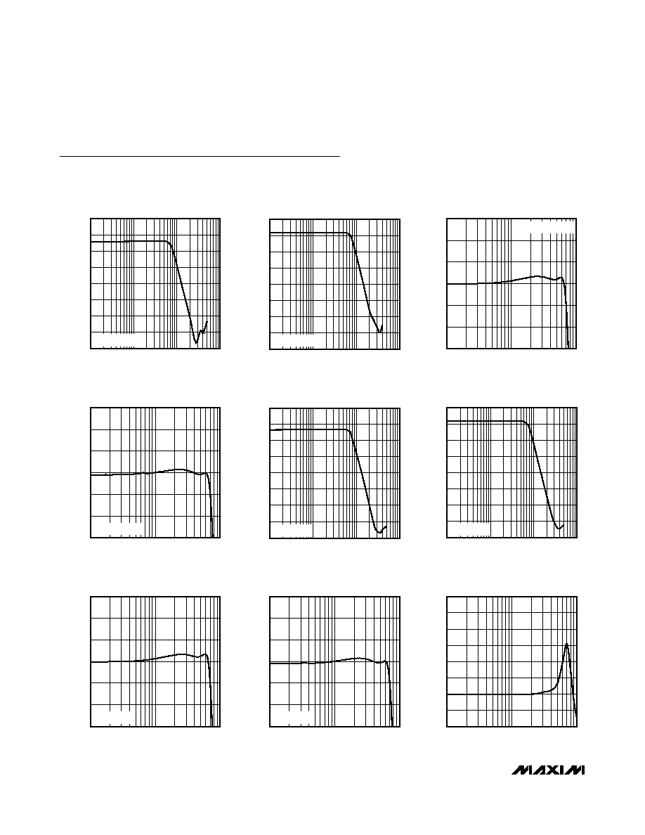
Typical Operating Characteristics
(V
CC
= SHDN = 3.0V, GND = 0V, R
L
= 150
to GND.)
MAX9502G
SMALL-SIGNAL BANDWIDTH
MAX9502 toc01
FREQUENCY (MHz)
RESPONSE (dB)
10
1
-50
-40
-30
-20
-10
0
10
20
-60
0.1
100
V
OUT
= 100mV
P-P
MAX9502M
SMALL-SIGNAL BANDWIDTH
MAX9502 toc02
FREQUENCY (MHz)
RESPONSE (dB)
10
1
-50
-40
-30
-20
-10
0
10
20
-60
0.1
100
V
OUT
= 100mV
P-P
MAX9502G
SMALL-SIGNAL GAIN FLATNESS
MAX9502 toc03
FREQUENCY (MHz)
RESPONSE (dB)
1
4
5
6
7
8
9
3
0.1
10
V
OUT
= 100mV
P-P
MAX9502M
SMALL-SIGNAL GAIN FLATNESS
MAX9502 toc04
FREQUENCY (MHz)
RESPONSE (dB)
1
10
11
12
13
14
15
9
0.1
10
V
OUT
= 100mV
P-P
MAX9502G
LARGE-SIGNAL BANDWIDTH
MAX9502 toc05
FREQUENCY (MHz)
RESPONSE (dB)
10
1
0.1
100
V
OUT
= 2V
P-P
-50
-40
-30
-20
-10
0
10
20
-60
MAX9502M
LARGE-SIGNAL BANDWIDTH
MAX9502 toc06
FREQUENCY (MHz)
RESPONSE (dB)
10
1
-50
-40
-30
-20
-10
0
10
20
-60
0.1
100
V
OUT
= 2V
P-P
MAX9502G
LARGE-SIGNAL GAIN FLATNESS
MAX9502 toc07
FREQUENCY (MHz)
RESPONSE (dB)
1
4
5
6
7
8
9
3
0.1
10
V
OUT
= 2V
P-P
MAX9502M
LARGE-SIGNAL GAIN FLATNESS
MAX9502 toc08
FREQUENCY (MHz)
RESPONSE (dB)
1
10
11
12
13
14
15
9
0.1
10
V
OUT
= 2V
P-P
MAX9502G
GROUP DELAY
MAX9502 toc09
FREQUENCY (MHz)
DELAY (ns)
1
60
80
100
120
140
160
180
200
40
0.1
10

MAX9502
2.5V Video Amplifier with Reconstruction Filter
_______________________________________________________________________________________
5
MAX9502M
GROUP DELAY
MAX9502 toc10
FREQUENCY (MHz)
DELAY (ns)
1
60
80
100
120
140
160
180
200
40
0.1
10
MAX9502G
POWER-SUPPLY REJECTION RATIO
MAX9502 toc11
FREQUENCY (MHz)
RESPONSE (dB)
1
0.1
0.001
0.01
-90
-80
-70
-50
-60
-40
-30
-20
-10
0
-100
0.0001
10
MAX9502M
POWER-SUPPLY REJECTION RATIO
MAX9502 toc12
FREQUENCY (MHz)
RESPONSE (dB)
1
0.1
0.001
0.01
-90
-70
-80
-60
-50
-40
-30
-20
-10
0
-100
0.0001
10
SUPPLY CURRENT vs. TEMPERATURE
MAX9502 toc13
TEMPERATURE (
∞C)
SUPPLY CURRENT (mA)
60
35
-15
10
3.5
4.0
4.5
5.0
5.5
6.0
6.5
7.0
3.0
-40
85
MAX9502G
MAX9502M
SUPPLY CURRENT
vs. SHDN INPUT VOLTAGE
MAX9502 toc14
SHDN INPUT VOLTAGE (V)
SUPPLY CURRENT (mA)
2.5
2.0
1.5
1.0
0.5
0.5
1.0
1.5
2.0
2.5
3.0
3.5
4.0
4.5
5.0
5.5
6.0
0
0
3.0
V
SHDN
= RISING
SHUTDOWN LOGIC THRESHOLD
vs. SUPPLY VOLTAGE
MAX9502 toc15
SUPPLY VOLTAGE (V)
SHUTDOWN LOGIC THRESHOLD (V)
3.5
3.4
3.3
3.2
3.1
3.0
2.9
2.8
2.7
2.6
0.5
1.0
1.5
2.0
2.5
3.0
0
2.5
3.6
V
SHDN
= RISING
MAX9502G
VOLTAGE GAIN vs. TEMPERATURE
MAX9502 toc16
TEMPERATURE (
∞C)
GAIN (dB)
60
35
10
-15
5.7
5.9
6.1
6.3
6.5
5.5
-40
85
MAX9502M
VOLTAGE GAIN vs. TEMPERATURE
MAX9502 toc17
TEMPERATURE (
∞C)
GAIN (dB)
60
35
10
-15
11.7
11.9
12.1
12.3
12.5
11.5
-40
85
MAX9502G
DIFFERENTIAL GAIN AND PHASE
MAX9502 toc18
DIFFERENTIAL GAIN (%)
6
5
4
3
2
0.2
0.1
-0.3
-0.1
0.4
-0.4
1
7
DIFFERENTIAL PHASE (deg)
6
5
4
3
2
0.4
0
-0.4
0.8
-0.8
1
7
Typical Operating Characteristics (continued)
(V
CC
= SHDN = 3.0V, GND = 0V, R
L
= 150
to GND.)