Äîêóìåíòàöèÿ è îïèñàíèÿ www.docs.chipfind.ru

General Description
The MAX9595 dual SCART switch matrix routes audio
and video signals between an MPEG encoder and two
external SCART connectors under I
2
C
control, and
meets the requirements of EN50049-1, IEC 933-1,
Canal+, and BSkyB standards.
The video and audio channels feature input source
selection multiplexers, input buffers, and output buffers
for routing all inputs to selected outputs.
The MAX9595 provides programmable gain control from
+5dB to +7dB in 1dB steps for red, green, and blue com-
ponent video signals. All other video outputs have a fixed
+6dB gain. Additional features include an internal luma
and chroma (Y/C) mixer that generates a composite
video signal (CVBS) to supply an RF modulator output,
and internal video reconstruction lowpass filters with a
cutoff frequency of 6MHz. The MAX9595 TV audio chan-
nel features clickless switching and programmable vol-
ume control from -56dB to +6dB in 2dB steps. The VCR
audio output also has programmable gain for -6dB, 0dB,
or +6dB. The device also generates monaural audio from
left and right stereo inputs. All audio drivers deliver a
3.0V
RMS
minimum output.
The MAX9595 operates with standard 5V and 12V
power supplies and supports slow-switching and fast-
switching signals. The I
2
C interface programs the
gain and volume control, and selects the input source
for routing.
The MAX9595 is available in a compact 48-pin thin
QFN package and is specified over the 0°C to +70°C
commercial temperature range.
Applications
Satellite Set-Top Boxes
Cable Set-Top Boxes
TVs
VCRs
DVDs
Features
Video Outputs Drive 2V
P-P
into 150
Audio Outputs Drive 3V
RMS
into 10k
Clickless, Popless Audio Gain Control and
Switching
Interrupt Output Detects Changes on Slow
Switching Input
AC-Coupled Video Inputs with Internal Clamp and
Bias
DC-Coupled Video Outputs
Composite Video Signal Created Internally from
Y/C Inputs
Internal Video Reconstruction Filters Provide
-50dB at 27MHz
Single-Ended Audio Input
Red/Chroma Switch for Bidirectional I/O
I
2
C-Programmable RGB Gain from +5dB to +7dB
I
2
C-Programmable Audio Gain Control from +6dB
to -56dB
Meets EN50049-1, IEC 933-1, Canal+, and BSkyB
Requirements
MAX9595
Audio/Video Switch for Dual SCART Connector
________________________________________________________________ Maxim Integrated Products
1
Ordering Information
19-3946; Rev 0; 1/06
For pricing, delivery, and ordering information, please contact Maxim/Dallas Direct! at
1-888-629-4642, or visit Maxim's website at www.maxim-ic.com.
Pin Configuration and Typical Application Circuit appear at
end of data sheet.
System Block Diagram appears at end of data sheet.
EVALUATION KIT
AVAILABLE
Purchase of I
2
C components from Maxim Integrated Products,
Inc. or one of its sublicensed Associated Companies, conveys
a license under the Philips I
2
C Patent Rights to use these com-
ponents in an I
2
C system, provided that the system conforms to
the I
2
C Standard Specification as defined by Philips.
PART
TEMP RANGE
PIN-
PACKAGE
PKG
CODE
MAX9595CTM+
0°C to +70°C
48 Thin QFN-EP*
(7mm x 7mm)
T4877-6
*EP = Exposed paddle.
+Denotes lead-free package.
MAX9595
Audio/Video Switch for Dual SCART Connector
2
_______________________________________________________________________________________
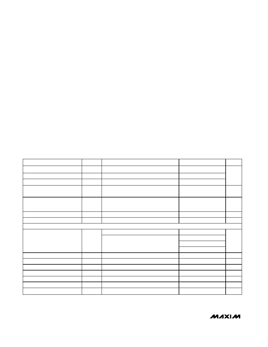
ABSOLUTE MAXIMUM RATINGS
ELECTRICAL CHARACTERISTICS
(V
12
= 12V, V
VID
= V
AUD
= 5V; 0.1µF X5R capacitor in parallel with a 10µF aluminum electrolytic capacitor from V
AUD
to GNDAUD,
V
12
to GNDAUD, and V
VID
to GNDVID; SET = 100k nominal, R
LOAD
= 150, T
A
= 0°C to +70°C, unless otherwise noted. Typical
values are at T
A
= +25°C.) (Note 1)
Stresses beyond those listed under "Absolute Maximum Ratings" may cause permanent damage to the device. These are stress ratings only, and functional
operation of the device at these or any other conditions beyond those indicated in the operational sections of the specifications is not implied. Exposure to
absolute maximum rating conditions for extended periods may affect device reliability.
V
VID
to GNDVID........................................................-0.3V to +6V
V
12
to GNDAUD .....................................................-0.3V to +14V
V
AUD
to GNDAUD ....................................................-0.3V to +6V
GNDAUD to GNDVID ............................................-0.1V to +0.1V
All Video Inputs, ENCIN_FS, VCRIN_FS,
SET to GNDVID......................................-0.3V to (V
VID
+ 0.3V)
All Audio Inputs,
AUDBIAS to GNDAUD .........................-0.3V to (V
AUD
+ 0.3V)
SDA, SCL, DEV_ADDR,
INTERRUPT_OUT to GNDVID ..............................-0.3V to +6V
All Audio Outputs, TV_SS,
VCR_SS to GNDAUD...............................-0.3V to (V
12
+ 0.3V)
INTERRUPT_OUT Current ................................................+50mA
All Video Outputs, TVOUT_FS to V
VID
, V
AUD
,
GNDAUD, GNDVID ................................................Continuous
All Audio Outputs to V
VID
, V
AUD
, V
12
,
GNDVID, GNDAUD ................................................Continuous
Continuous Power Dissipation (T
A
= +70°C)
48-Pin Thin QFN (derate 27mW/°C above +70°C) .....2105.3mW
Operating Temperature Range...............................0°C to +70°C
Junction Temperature ......................................................+150°C
Storage Temperature Range .............................-65°C to +150°C
Lead Temperature (soldering, 10s) .................................+300°C
PARAMETER
SYMBOL
CONDITIONS
MIN
TYP
MAX
UNITS
V
VID
Supply Voltage Range
V
VID
Inferred from video gain test
4.75
5.0
5.25
V
AUD
Supply Voltage Range
V
AUD
Inferred from audio gain test
4.75
5.0
5.25
V
12
Supply Voltage Range
V
12
Inferred from slow switching levels
11.4
12.0
12.6
V
V
VID
Quiescent Supply Current
I
VID_Q
All video output amplifiers are enabled,
no load
69
100
mA
V
VID
Standby Supply Current
I
VID_Q
All video output amplifiers are in shutdown,
and TV_FS_OUT driver is in shutdown, no
load
40
60
mA
V
AUD
Quiescent Supply Current
I
AUD_Q
No load
2.4
6
mA
V
12
Quiescent Supply Current
I
12_Q
No load
3.6
6
mA
VIDEO CHARACTERISTICS
CVBS and Y-C, 1V
P-P
input
+5.5
+6.0
+6.5
+4.5
+5.0
+5.5
+5.5
+6.0
+6.5
Voltage Gain
G_V
RGB, 1V
P-P
input, (programmable gain
control)
+6.5
+7.0
+7.5
dB
LP Filter Attenuation
ATTN
T
A
= +25°C, f = 6MHz, V
IN
= 1V
P-P
1.2
3.3
dB
LP Filter Suppression
SPPR
T
A
= +25°C, f = 27MHz, V
IN
= 1V
P-P
35
50
dB
Slew Rate
SR
V
OUT
= 2V
P-P
8
V/µs
Settling Time
t
S
V
OUT
= 2V
P-P
, settle to 0.1% (Note 2)
380
ns
Gain Matching
AG
1V
P-P
input, between RGB or Y-C
-0.5
+0.5
dB
Differential Gain
DG
5-step modulated staircase
0.4
%
Differential Phase
DP
5-step modulated staircase
0.2
degrees
MAX9595
Audio/Video Switch for Dual SCART Connector
_______________________________________________________________________________________
3
ELECTRICAL CHARACTERISTICS (continued)
(V
12
= 12V, V
VID
= V
AUD
= 5V; 0.1µF X5R capacitor in parallel with a 10µF aluminum electrolytic capacitor from V
AUD
to GNDAUD,
V
12
to GNDAUD, and V
VID
to GNDVID; SET = 100k nominal, R
LOAD
= 150, T
A
= 0°C to +70°C, unless otherwise noted. Typical
values are at T
A
= +25°C.) (Note 1)
PARAMETER
SYMBOL
CONDITIONS
MIN
TYP
MAX
UNITS
Signal-to-RMS Noise
SNR_V
V
IN
= 1V
P-P
65
dB
Group Delay Variation
GD
f = 0.1MHz to 4.43MHz
14
ns
Sync-Tip Clamp Level
V_CLMP
RGB, composite, and luma input, no signal,
no load
1.21
V
Chroma Bias
V_BIAS
Chroma input only, no signal, no load
1.9
V
Droop
D
Set by input current
-2
+2
%
Power-Supply Rejection Ratio
PSRR_V
DC, 0.5V
P-P
48
dB
CVBS or RGB video inputs, V
IN
> V_CLMP
4
M
Input Impedance
Z
IN
Chroma video input. V
IN
= V_BIAS
11
k
Input Clamp Current
I
CLMP
V
IN
= 1.75V
2.5
5
8.0
µA
Pulldown Resistance
RP
Enable VCR_R/C_OUT and TV_R/C_OUT
pulldown through I
2
C, (see registers 7 and 9
for loading register details)
10
RGB, composite, and luma, no signal,
no load
1.08
Output Pin Bias Voltage
V
OUT
Chroma, no signal, no load
2.27
V
Crosstalk
XTLK
Between any two active inputs, f = 4.43MHz,
V
IN
= 1V
P-P
-50
dB
Mute Suppression
M_SPR_V
f = 4.43MHz, V
IN
= 1V
P-P
, on one input only
-50
dB
AUDIO CHARACTERISTICS (Note 3)
TV or VCR to stereo, gain = 0dB,
V
IN
= 1V
P-P
-0.5
0
+0.5
TV or VCR to mono, gain = 0dB, V
IN
= 1V
P-P
2.5
3.0
3.5
ENC to stereo, gain = 0dB, V
IN
= 1V
P-P
3.02
3.52
4.02
Voltage Gain (Measured From
Application Input)
G_A
ENC to mono, gain = 0dB, V
IN
= 1V
P-P
6.02
6.52
7.02
dB
Gain Matching Between
Channels
G_A
Gain = 0dB, V
IN
= 1V
P-P
-0.5
0
+0.5
dB
Flatness
A
f = 20Hz to 20kHz, 0.5V
RMS
input,
gain = 0dB
0.01
dB
Frequency Bandwidth
BW
0.5V
RMS
input, frequency where output is
-3dB referenced to 1kHz
230
kHz
Input DC Level (Excluding
Encoder Inputs which are Hi-Z)
V
IN
Gain = 0dB
0.2308
x V
12
V

MAX9595
Audio/Video Switch for Dual SCART Connector
4
_______________________________________________________________________________________
ELECTRICAL CHARACTERISTICS (continued)
(V
12
= 12V, V
VID
= V
AUD
= 5V; 0.1µF X5R capacitor in parallel with a 10µF aluminum electrolytic capacitor from V
AUD
to GNDAUD,
V
12
to GNDAUD, and V
VID
to GNDVID; SET = 100k nominal, R
LOAD
= 150, T
A
= 0°C to +70°C, unless otherwise noted. Typical
values are at T
A
= +25°C.) (Note 1)
PARAMETER
SYMBOL
CONDITIONS
MIN
TYP
MAX
UNIT
Single-ended inputs, f = 1kHz, THD < 1%
3
Input Signal Amplitude
(Measured from Application
Input)
V
IN_AC
ENC inputs single-ended, f = 1kHz,
THD < 1%
1.31
V
RMS
Single ended: VCR_INR, VCR_INL, TV_INR,
TV_INL
0.1
Input Resistance (Measured at
Parts Input)
R
IN
Encoder, ENC
_
INL, ENC_INR
0.1
M
Output DC Level
V
OUT_DC
V
IN
= 0V
0.5 x
V
12
V
Signal-to-Noise Ratio (Measured
from Application Input)
SNR_A
f = 1.0kHz, 1V
RMS
application input,
gain = 0dB, 20Hz to 20kHz
95
dB
R
LOAD
= 10k, f = 1.0kHz, 0.5V
RMS
output
0.004
Total Harmonic Distortion Plus
Noise
THD+N
R
LOAD
= 10k, f = 1.0kHz, 2V
RMS
output
0.004
%
Output Impedance
ZO
f = 1kHz
1
1.414V
P-P
input, programmable gain to TV
SCART volume control range extends from
-56dB to +6dB
1.5
2
2.5
Volume Attenuation Step
ASTEP
1.414V
P-P
input, programmable gain to VCR
audio extends from -6dB to +6dB
5.5
6
6.5
dB
From V
12,
f = 1kHz, 0.5V
P-P
,
(C
AUD_BIAS
= 47µF), gain = 0dB
75
Power-Supply Rejection Ratio
PSRR_A
From V
AUD
, f = 1kHz, 0.5V
P-P,
V
AUD
+4.75V, V
AUD
+5.25V, gain = 0dB
75
dB
Mute Suppression
M_SPR_A
f = 1kHz, 0.5V
RMS
input, set through I
2
C, see
register 1 for loading register details
90
dB
Audio Clipping Level
VCLIP
f = 1kHz, 2.5V
RMS
input, gain = 6dB,
THD < 1%
3.6
V
RMS
Left-to-Right Crosstalk
XTLK_LR
f = 1kHz, 0.5V
RMS
input, gain = 0dB
80
dB
Crosstalk
XTLK_CC
TV SCART to VCR SCART or VCR SCART to
TV SCART, f = 1kHz, 0.5V
RMS
input, gain =
0dB
90
dB
MAX9595
Audio/Video Switch for Dual SCART Connector
_______________________________________________________________________________________
5
ELECTRICAL CHARACTERISTICS (continued)
(V
12
= 12V, V
VID
= V
AUD
= 5V; 0.1µF X5R capacitor in parallel with a 10µF aluminum electrolytic capacitor from V
AUD
to GNDAUD,
V
12
to GNDAUD, and V
VID
to GNDVID; SET = 100k nominal, R
LOAD
= 150, T
A
= 0°C to +70°C, unless otherwise noted. Typical
values are at T
A
= +25°C.) (Note 1)
PARAMETER
SYMBOL
CONDITIONS
MIN
TYP
MAX
UNIT
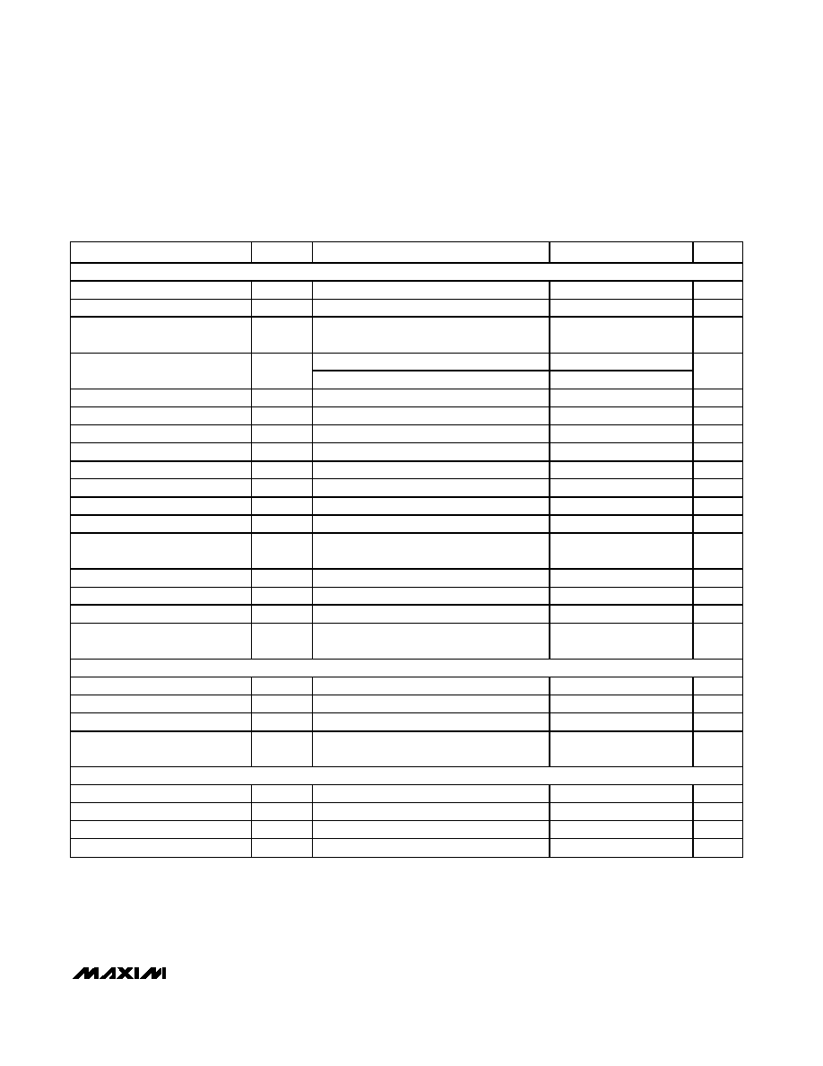
DIGITAL INTERFACE: SDA and SCL (Note 4)
Low-Level Input Voltage
V
IL
0
0.8
V
High-Level Input Voltage
V
IH
2.6
V
Hysteresis of Schmitt Trigger
Input
0.2
V
I
SINK
= 3mA
0.4
SDA Low-Level Output Voltage
V
OL
I
SINK
= 6mA
0.6
V
Output Fall Time for SDA Line
400pF bus load
250
ns
Spike Suppression
50
ns
Input Current
-10
+10
µA
Input Capacitance
5
pF
SCL Clock Frequency
0
400
kHz
Hold Time
t
HD,STA
0.6
µs
Low Period of SCL Clock
t
Low
1.3
µs
High Period of SCL Clock
t
HIGH
0.6
µs
Setup Time for a Repeated Start
Condition
t
SU,STA
0.6
µs
Data Hold Time
t
HD,DAT
0
0.9
µs
Data Setup Time
t
SU,DAT
100
ns
Setup Time for Stop Condition
t
SU,STO
0.6
µs
Bus Free Time Between a Stop
and Start
t
BUF
1.3
µs
OTHER DIGITAL PINS (Note 4)
DEV_ADDR Low Level
0.8
V
DEV_ADDR High Level
2.6
V
INTERRUPT_OUT Low Voltage
INTERRUPT_OUT sinking 1mA
0.15
0.4
V
INTERRUPT_OUT High Leakage
Current
V
INTERRUPT_OUT
= 5V
1
10
µA
SLOW SWITCHING SECTION (Note 4)
Input Low Level
0
2
V
Input Medium Level
4.5
7.0
V
Input High Level
9.5
V
12
V
Input Current
50
100
µA