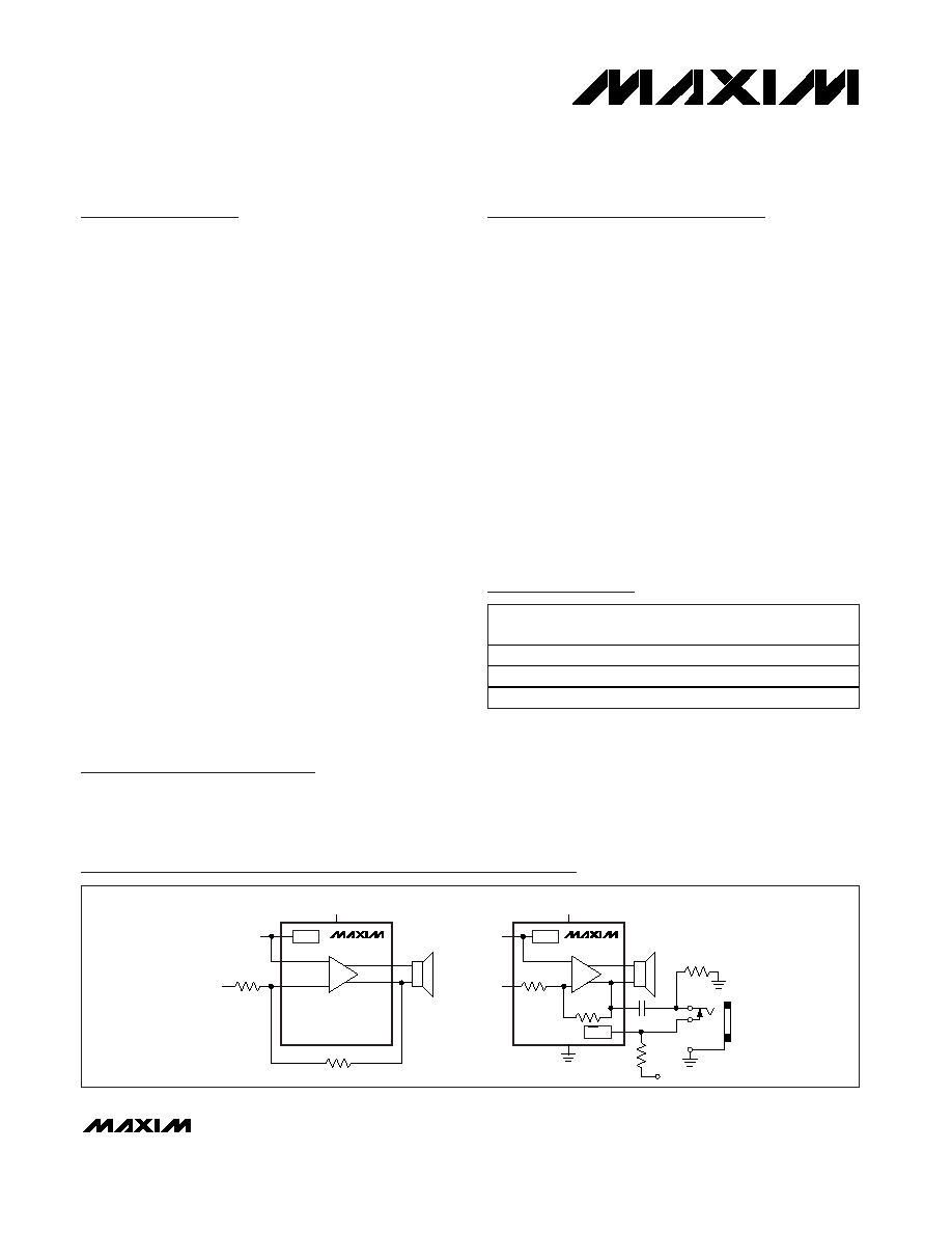
General Description
The MAX9716/MAX9717 audio power amplifiers are ideal
for portable audio devices with internal speakers. A
bridge-tied load (BTL) architecture minimizes external
component count, while providing high-quality audio
reproduction. Both devices deliver 1.4W continuous
power into a 4
load with less than 1% Total Harmonic
Distortion (THD) while operating from a single +5V sup-
ply. With an 8
load, both devices deliver 1W continuous
power. These devices also deliver 350mW continuous
power into an 8
load while operating from a single
+3.0V supply. The devices are available as adjustable
gain amplifiers (MAX9716/MAX9717A) or with internally
fixed gains of 6dB, 9dB, and 12dB (MAX9717B/
MAX9717C/MAX9717D), reducing component count.
A low-power shutdown mode disables the bias generator
and amplifiers, reducing quiescent current consumption
to less than 10nA. These devices feature Maxim's
industry-leading, comprehensive click-and-pop sup-
pression that reduces audible clicks and pops during
startup and shutdown.
The MAX9717 features a headphone sense input (BTL/SE)
that senses when a headphone is connected to the
device, disables the BTL slave driver, muting the speaker
while driving the headphone as a single-ended load.
The MAX9716 is pin compatible with the LM4890 and is
available in 9-bump UCSPTM, 8-pin TDFN (3mm x
3mm), and 8-pin µMAX packages. The MAX9717 is
available in 9-bump UCSP, 8-pin TDFN, and 8-pin
µMAX packages. Both devices operate over the -40∞C
to +85∞C extended temperature range.
Applications
Mobile Phones
PDAs
Portable Devices
Features
2.7V to 5.5V Single-Supply Operation
1.4W into 4
at 1% THD+N
10nA Low-Power Shutdown Mode
73dB PSRR at 1kHz
No Audible Clicks or Pops at Power-Up/Down
Internal Fixed Gain to Reduce Component Count
(MAX9717B/C/D)
Adjustable Gain Option (MAX9716/MAX9717A)
BTL
/SE Input Senses when Headphones are
Connected (MAX9717)
Pin Compatible with LM4890 (MAX9716)
Pin Compatible with TPA711 (MAX9717A)
Available in Compact, Thermally Enhanced
µ
MAX
and TDFN (3mm x 3mm) Packages
MAX9716/MAX9717
Low-Cost, Mono, 1.4W BTL Audio Power
Amplifiers
________________________________________________________________ Maxim Integrated Products
1
Ordering Information
V
CC
BTL/SE
BIAS
IN-
MAX9717B/C/D
SINGLE SUPPLY
2.7V TO 5.5V
BIAS
IN-
MAX9716
SINGLE SUPPLY
2.7V TO 5.5V
Simplified Block Diagrams
19-3146; Rev 0; 1/04
For pricing, delivery, and ordering information, please contact Maxim/Dallas Direct! at
1-888-629-4642, or visit Maxim's website at www.maxim-ic.com.
Pin Configurations and Selector Guide appear at end of data
sheet.
UCSP is a trademark of Maxim Integrated Products, Inc.
*Future product--contact factory for availability.
**EP = Exposed paddle.
PART
TEMP RANGE
PIN-
PACKAGE
GAIN
(dB)
MAX9716
ETA
-40∞C to +85∞C
8 TDFN-EP**
Adj.
MAX9716EBL-T*
-40∞C to +85∞C
3 x 3 UCSP
Adj.
MAX9716EUA
-40∞C to +85∞C
8 µMAX-EP**
Adj.
Ordering Information continued at end of data sheet.
MAX9716/MAX9717
Low-Cost, Mono, 1.4W BTL Audio Power
Amplifiers
2
_______________________________________________________________________________________
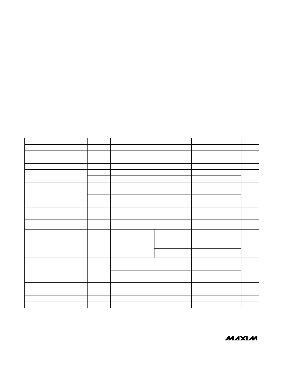
ABSOLUTE MAXIMUM RATINGS
ELECTRICAL CHARACTERISTICS--5V Supply
(V
CC
= 5V, GND = 0, SHDN = V
CC
, T
A
= +25∞C. C
BIAS
= 1µF, R
IN
= R
F
= 20k
(MAX9716/MAX9717A), IN+ = BIAS (MAX9716),
BTL/SE = GND (MAX9717_), R
L
=
connected between OUT+ and OUT-. Typical values are at T
A
= +25∞C.) (Note 2)
Stresses beyond those listed under "Absolute Maximum Ratings" may cause permanent damage to the device. These are stress ratings only, and functional
operation of the device at these or any other conditions beyond those indicated in the operational sections of the specifications is not implied. Exposure to
absolute maximum rating conditions for extended periods may affect device reliability.
Supply Voltage (V
CC
to GND) ..................................-0.3V to +6V
Any Other Pin to GND ...............................-0.3V to (V
CC
+ 0.3V)
IN_, BIAS, SHDN, BTL/SE Continuous Current...................20mA
OUT_ Short-Circuit Duration to GND or V
CC
(Note 1)...Continuous
Continuous Power Dissipation (T
A
= +70∞C)
8-Pin TDFN (derate 24.4mW/∞C above +70∞C) .........1951mW
8-Pin µMAX (derate 10.3mW/∞C above +70∞C) ...........825mW
9-Bump UCSP (derate 5.2mW/∞C above 70∞C) ...........412mW
Operating Temperature Range ..........................-40∞C to +85∞C
Maximum Junction Temperature ....................................+150∞C
Storage Temperature Range .............................-65∞C to +150∞C
Lead Temperature (soldering, 10s) .................................+300∞C
Bump Temperature (soldering)........................................+235∞C
PARAMETER
SYMBOL
CONDITIONS
MIN
TYP
MAX
UNITS
Supply Voltage
V
CC
Inferred by PSRR test
2.7
5.5
V
Quiescent Supply Current
I
CC
V
IN-
= V
IN+
= V
BIAS
(Note 3),
T
A
= -40∞C to +85∞C
4.3
8
mA
Shutdown Supply Current
I
SHDN
SHDN = GND
0.01
1
µA
V
IH
1.2
SHDN Threshold
V
IL
0.4
V
V
IH
0.9 x
V
CC
BTL/SE Threshold
V
IL
0.7 x
V
CC
V
Common-Mode Bias Voltage
V
BIAS
(Note 4)
V
CC
/2
- 6%
V
CC
/2
V
CC
/2
+ 6%
V
Output Offset Voltage
V
OS
V
IN-
= V
OUT+
, V
IN+
= V
BIAS
(Note 5)
±7
±15
mV
V
CC
= 2.7V to 5.5V
DC, V
BIAS
= 1.5V
60
80
f = 217Hz
61
Power-Supply Rejection Ratio
PSRR
V
IN+
= V
BIAS
,
V
RIPPLE
= 200mV
P-P
,
R
L
= 8
(Note 6)
f = 1kHz
73
dB
R
L
= 8
, THD+N = 1%, f
IN
= 1kHz (Note 7)
0.8
1.1
R
L
= 4
, THD+N = 1%, f
IN
= 1kHz (Note 7)
1.4
Output Power
P
OUT
R
L
= 16
, BTL/SE = V
CC
(single-ended
mode), THD+N = 1%, f
IN
= 1kHz
0.155
W
Total Harmonic Distortion Plus
Noise
THD+N
A
V
= 6dB, R
L
= 8
, f
IN
= 1kHz,
P
OUT
= 0.5W (Note 8)
0.024
%
Output Noise Density
e
n
f
IN
= 10kHz
106
nV/
Hz
Signal-to-Noise Ratio
SNR
THD+N = 1%
105
dB

MAX9716/MAX9717
Low-Cost, Mono, 1.4W BTL Audio Power
Amplifiers
_______________________________________________________________________________________
3
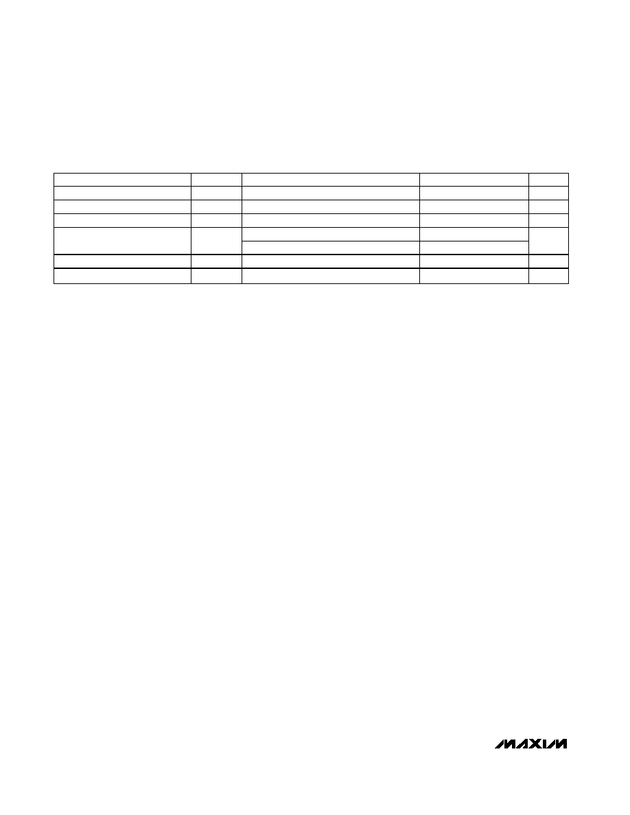
ELECTRICAL CHARACTERISTICS--5V Supply (continued)
(V
CC
= 5V, GND = 0, SHDN = V
CC
, T
A
= +25∞C. C
BIAS
= 1µF, R
IN
= R
F
= 20k
(MAX9716/MAX9717A), IN+ = BIAS (MAX9716),
BTL/SE = GND (MAX9717_), R
L
=
connected between OUT+ and OUT-. Typical values are at T
A
= +25∞C.) (Note 2)
PARAMETER
SYMBOL
CONDITIONS
MIN
TYP
MAX
UNITS
Output Short-Circuit Current Limit
I
SC
(Note 9)
1.1
A
Thermal Shutdown Threshold
+160
∞C
Thermal Shutdown Hysteresis
15
∞C
250
Power-Up/Enable from Shutdown
Time (Note 10)
t
PU
C
BIAS
= 0.1µF
25
ms
Shutdown Time
t
SHDN
5
µs
Input Resistance
R
IN
MAX9717B/C/D
12
20
28
k
ELECTRICAL CHARACTERISTICS--3V Supply
(V
CC
= 3V, GND = 0, SHDN = V
CC
, T
A
= +25∞C. C
BIAS
= 1µF, R
IN
= R
F
= 20k
(MAX9716/MAX9717A), IN+ = BIAS (MAX9716),
BTL/SE = GND (MAX9717_), R
L
=
connected between OUT+ and OUT-. Typical values are at T
A
= +25∞C.) (Note 2)
PARAMETER
SYMBOL
CONDITIONS
MIN
TYP
MAX
UNITS
Quiescent Supply Current
I
CC
V
IN-
= V
IN+
= V
BIAS
(Note 3),
T
A
= -40∞C to +85∞C
4
8.0
mA
Shutdown Supply Current
I
SHDN
SHDN = GND
0.01
1
µA
V
IH
1.2
SHDN Threshold
V
IL
0.4
V
V
IH
0.9 x
V
CC
BTL/SE Threshold
V
IL
0.7 x
V
CC
V
Common-Mode Bias Voltage
V
BIAS
(Note 4)
V
CC
/2
- 9%
V
CC
/2
V
CC
/2
+ 9%
V
Output Offset Voltage
V
OS
V
IN-
= V
OUT+
, V
IN+
= V
BIAS
(Note 5)
±7
±15
mV
f = 217Hz
61
Power-Supply Rejection Ratio
PSRR
V
IN+
= V
BIAS
,
V
RIPPLE
= 200mV
P-P
,
R
L
= 8
(Note 6)
f = 1kHz
73
dB
R
L
= 8
, THD+N = 1%, f
IN
= 1kHz (Note 7)
350
Output Power
P
OUT
R
L
= 4
, THD+N = 1%, f
IN
= 1kHz (Note 7)
525
mW
Total Harmonic Distortion Plus
Noise
THD+N
A
V
= 6dB, R
L
= 8
, f
IN
= 1kHz,
P
OUT
= 0.5W, V
CC
= 3V (Note 8)
0.024
%
Output-Noise Density
e
n
f
IN
= 10kHz
106
nV/
Hz
Signal-to-Noise Ratio
SNR
THD+N = 1%
100
dB
MAX9716/MAX9717
Low-Cost, Mono, 1.4W BTL Audio Power
Amplifiers
4
_______________________________________________________________________________________
ELECTRICAL CHARACTERISTICS--3V Supply (continued)
(V
CC
= 3V, GND = 0, SHDN = V
CC
, T
A
= +25∞C. C
BIAS
= 1µF, R
IN
= R
F
= 20k
(MAX9716/MAX9717A), IN+ = BIAS (MAX9716),
BTL/SE = GND (MAX9717_), R
L
=
connected between OUT+ and OUT-. Typical values are at T
A
= +25∞C.) (Note 2)
PARAMETER
SYMBOL
CONDITIONS
MIN
TYP
MAX
UNITS
Output Short-Circuit Current Limit
I
SC
(Note 9)
1.1
A
Thermal Shutdown Threshold
+160
∞C
Thermal Shutdown Hysteresis
15
∞C
250
Power-Up/Enable from Shutdown
Time (Note 10)
t
PU
C
BIAS
= 0.1µF
25
ms
Shutdown Time
t
SHDN
5
µs
Input Resistance
R
IN
MAX9717B/C/D
12
20
28
k
Note 1:
Continuous power dissipation must also be observed.
Note 2:
All specifications are tested at T
A
= +25∞C. Specifications over temperature (T
A
= T
MIN
to T
MAX
) are not production tested,
and guaranteed by design.
Note 3:
Quiescent power-supply current is specified and tested with no load. Quiescent power-supply current depends on the off-
set voltage when a practical load is connected to the amplifier.
Note 4:
Common-mode bias voltage is the voltage on BIAS and is nominally V
CC
/2.
Note 5:
V
OS
= V
OUT+
- V
OUT-.
Note 6:
The amplifier input IN- is AC-coupled to GND through C
IN
.
Note 7:
Output power is specified by a combination of a functional output current test and characterization analysis.
Note 8:
Measurement bandwidth for THD+N is 22Hz to 22kHz.
Note 9:
Extended short-circuit conditions result in a pulsed output.
Note 10:
Time for V
OUT
to rise to 50% of final DC value.

MAX9716/MAX9717
Low-Cost, Mono, 1.4W BTL Audio Power
Amplifiers
_______________________________________________________________________________________
5
TOTAL HARMONIC DISTORTION
PLUS NOISE vs. FREQUENCY
MAX9716 toc01
FREQUENCY (Hz)
THD+N (%)
10k
1k
100
0.01
0.1
1
10
100
0.001
10
100k
V
CC
= 5V
R
L
= 8
A
V
= 6dB
OUTPUT POWER = 800mW
OUTPUT POWER = 30mW
TOTAL HARMONIC DISTORTION
PLUS NOISE vs. FREQUENCY
MAX9716 toc02
FREQUENCY (Hz)
THD+N (%)
10k
1k
100
0.01
0.1
1
10
100
0.001
10
100k
V
CC
= 5V
R
L
= 8
A
V
= 12dB
OUTPUT POWER = 800mW
OUTPUT POWER = 200mW
TOTAL HARMONIC DISTORTION
PLUS NOISE vs. FREQUENCY
MAX9716 toc03
FREQUENCY (Hz)
THD+N (%)
10k
1k
100
0.01
0.1
1
10
100
0.001
10
100k
V
CC
= 3V
R
L
= 8
A
V
= 6dB
OUTPUT POWER = 250mW
OUTPUT POWER = 30mW
TOTAL HARMONIC DISTORTION
PLUS NOISE vs. FREQUENCY
MAX9716 toc04
FREQUENCY (Hz)
THD+N (%)
10k
1k
100
0.01
0.1
1
10
100
0.001
10
100k
V
CC
= 3V
R
L
= 8
A
V
= 12dB
OUTPUT POWER = 200mW
OUTPUT POWER = 50mW
TOTAL HARMONIC DISTORTION
PLUS NOISE vs. FREQUENCY
MAX9716 toc05
FREQUENCY (Hz)
THD+N (%)
10k
1k
100
0.01
0.1
1
10
100
0.001
10
100k
V
CC
= 5V
R
L
= 4
A
V
= 6dB
OUTPUT POWER = 1W
OUTPUT POWER = 200mW
TOTAL HARMONIC DISTORTION
PLUS NOISE vs. FREQUENCY
MAX9716 toc06
FREQUENCY (Hz)
THD+N (%)
10k
1k
100
0.01
0.1
1
10
100
0.001
10
100k
V
CC
= 5V
R
L
= 4
A
V
= 12dB
OUTPUT POWER = 250mW
OUTPUT POWER = 1W
TOTAL HARMONIC DISTORTION
PLUS NOISE vs. FREQUENCY
MAX9716 toc07
FREQUENCY (Hz)
THD+N (%)
10k
1k
100
0.01
0.1
1
10
100
0.001
10
100k
V
CC
= 3V
R
L
= 4
A
V
= 6dB
OUTPUT POWER = 50mW
OUTPUT POWER = 350mW
TOTAL HARMONIC DISTORTION
PLUS NOISE vs. FREQUENCY
MAX9716 toc08
FREQUENCY (Hz)
THD+N (%)
10k
1k
100
0.01
0.1
1
10
100
0.001
10
100k
V
CC
= 3V
R
L
= 4
A
V
= 12dB
OUTPUT POWER = 50mW
OUTPUT POWER = 350mW
TOTAL HARMONIC DISTORTION PLUS
NOISE vs. FREQUENCY (SINGLE-ENDED)
MAX9716 toc09
FREQUENCY (Hz)
THD+N (%)
10k
1k
100
0.001
0.01
0.1
1
10
100
0.0001
10
100k
V
CC
= 5V
R
L
= 16
A
V
= 12dB
OUTPUT POWER = 125mW
OUTPUT POWER = 25mW
Typical Operating Characteristics
(V
CC
= 5V, THD+N measurement bandwidth = 22Hz to 22kHz, BTL mode, T
A
= +25∞C, unless otherwise noted.)