 | –≠–ª–µ–∫—Ç—Ä–æ–Ω–Ω—ã–π –∫–æ–º–ø–æ–Ω–µ–Ω—Ç: MAX9751 | –°–∫–∞—á–∞—Ç—å:  PDF PDF  ZIP ZIP |
General Description
The MAX9750/MAX9751/MAX9755 combine a stereo,
2.6W audio power amplifier and stereo DirectDrive
110mW headphone amplifier in a single device. The
headphone amplifier uses Maxim's patented DirectDrive
architecture that produces a ground-referenced output
from a single supply, eliminating the need for large DC-
blocking capacitors, saving cost, space, and component
height. A high 90dB PSRR and low 0.01% THD+N
ensures clean, low-distortion amplification of the audio
signal.
The MAX9750 features an analog volume control, and a
BEEP input. The MAX9751 features a 2:1 input multiplexer,
allowing multiple audio sources to be selected. All devices
feature a single-supply voltage, a shutdown mode, logic-
selectable gain, and a headphone sense input. Industry-
leading click-and-pop suppression eliminates audible
transients during power and shutdown cycles.
The MAX9750/MAX9751/MAX9755 are offered in space-
saving, thermally efficient 28-pin thin QFN (5mm x 5mm
x 0.8mm) and 28-pin TSSOP-EP packages. Both devices
have thermal-overload and output short-circuit protec-
tion, and are specified over the extended -40∞C to +85∞C
temperature range.
Applications
Notebook PCs
Flat-Panel TVs
Tablet PCs
PC Displays
Portable DVD
LCD Projectors
Features
No DC-Blocking Capacitors Required--Provides
Industry's Most Compact Notebook Audio
Solution
PC2001 Compliant
5V Single-Supply Operation
Class AB 2.6W Stereo BTL Speaker Amplifiers
110mW DirectDrive Headphone Amplifiers
High 90dB PSRR
Low-Power Shutdown Mode
Industry-Leading Click-and-Pop Suppression
Low 0.01% THD+N at 1kHz
Short-Circuit and Thermal Protection
Selectable Gain Settings
Analog Volume Control (MAX9750)
Beep Input with Glitch Filter (MAX9750)
2:1 Stereo Input MUX (MAX9751)
±8kV ESD-Protected Headphone Driver Outputs
Available in Space-Saving, Thermally Efficient
Packages
28-Pin Thin QFN (5mm x 5mm x 0.8mm)
28-Pin TSSOP-EP
MAX9750/MAX9751/MAX9755
2.6W Stereo Audio Power Amplifiers and
DirectDrive Headphone Amplifiers
________________________________________________________________ Maxim Integrated Products
1
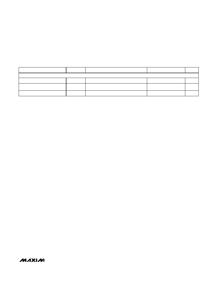
Ordering Information
19-3006; Rev 0; 1/04
For pricing, delivery, and ordering information, please contact Maxim/Dallas Direct! at
1-888-629-4642, or visit Maxim's website at www.maxim-ic.com.
PART
TEMP RANGE
PIN-
PACKAGE
M A XIM U M
G A I N ( d B )
MAX9750AETI*
-40∞C to +85∞C 28 Thi n QFN
13.5
MAX9750AEUI*
-40∞C to +85∞C 28 TSSOP-EP**
13.5
MAX9750BETI*
-40∞C to +85∞C 28 Thi n QFN
19.5
MAX9750BEUI*
-40∞C to +85∞C 28 TSSOP-EP**
19.5
MAX9750CETI
-40∞C to +85∞C 28 Thi n QFN
10.5
MAX9750CEUI*
-40∞C to +85∞C 28 TSSOP-EP**
10.5
MAX9751ETI*
-40∞C to +85∞C 28 Thi n QFN
10.5
MAX9751EUI*
-40∞C to +85∞C 28 TSSOP-EP**
10.5
MAX9755AETI*
-40∞C to +85∞C 28 Thi n QFN
10.5
MAX9755AEUI*
-40∞C to +85∞C 28 TSSOP-EP**
10.5
*Future product--contact factory for availability.
**EP = Exposed Paddle.
Lead-free package.
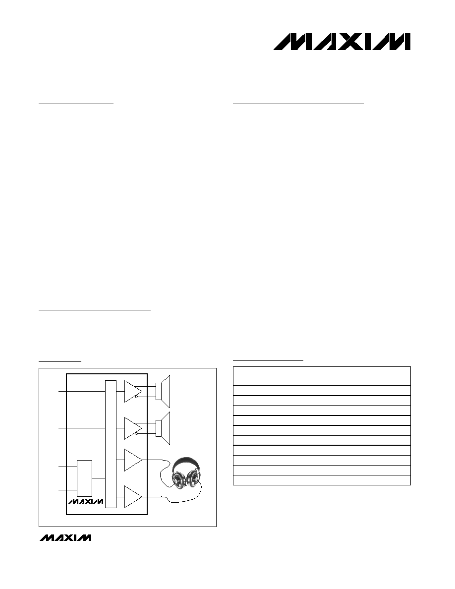
VOL
BEEP
MAX9750
Simplified Block Diagrams
Simplifed Block Diagrams continued at end of data sheet.
MAX9750/MAX9751/MAX9755
2.6W Stereo Audio Power Amplifiers and
DirectDrive Headphone Amplifiers
2
_______________________________________________________________________________________
ABSOLUTE MAXIMUM RATINGS
Stresses beyond those listed under "Absolute Maximum Ratings" may cause permanent damage to the device. These are stress ratings only, and functional
operation of the device at these or any other conditions beyond those indicated in the operational sections of the specifications is not implied. Exposure to
absolute maximum rating conditions for extended periods may affect device reliability.
Supply Voltage (V
DD
, PV
DD
, HPV
DD
, CPV
DD
to GND)..........+6V
GND to PGND.....................................................................±0.3V
CPV
SS
, C1N, V
SS
to GND .........................-6.0V to (GND + 0.3V)
HPOUT_ to GND ....................................................................±3V
Any Other Pin .............................................-0.3V to (V
DD
+ 0.3V)
Duration of OUT_ Short Circuit to GND or PV
DD
........Continuous
Duration of OUT_+ Short Circuit to OUT_- .................Continuous
Duration of HPOUT_ Short Circuit to GND,
V
SS
or HPV
DD
.........................................................Continuous
Continuous Current (PV
DD
, OUT_, PGND) ...........................1.7A
Continuous Current (CPV
DD
, C1N, C1P, CPV
SS
, V
SS
, HPV
DD
,
HPOUT_) .......................................................................850mA
Continuous Input Current (All Other Pins) ........................±20mA
Continuous Power Dissipation (T
A
= +70∞C)
28-Pin Thin QFN (derate 20.8mW/∞C above +70∞C) ..1667mW
28-Pin TSSOP-EP (derate 23.8mW/∞C above +70∞C).1904mW
Junction Temperature ......................................................+150∞C
Operating Temperature Range ...........................-40∞C to +85∞C
Storage Temperature Range .............................-65∞C to +150∞C
Lead Temperature (soldering, 10s) .................................+300∞C
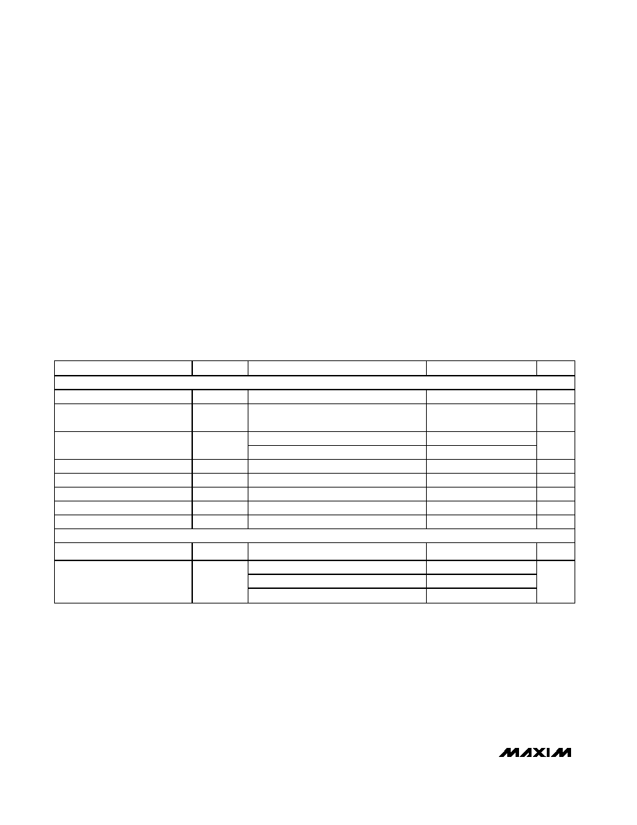
ELECTRICAL CHARACTERISTICS
(V
DD
= PV
DD
= CPV
DD
= HPV
DD
= 5V, GND = PGND = CPGND = 0V, SHDN = V
DD
, C
BIAS
= 1µF, C1 = C2 = 1µF, speaker load ter-
minated between OUT_+ and OUT_-, headphone load terminated between HPOUT_ and GND, MAX9750: GAIN1 = GAIN2 = VOL =
R
L
= 33k
= GND, MAX9751/MAX9755: GAIN = V
DD
= IN1/2 = GND, T
A
= T
MIN
to T
MAX
, unless otherwise noted. Typical values are
at T
A
= +25∞C.) (Note 1)
PARAMETER
SYMBOL
CONDITIONS
MIN
TYP
MAX
UNITS
GENERAL
Supply Voltage Range
V
DD
, PV
DD
Inferred from PSRR test
4.5
5.5
V
Headphone Supply Voltage
CPV
DD
,
HPV
DD
Inferred from PSRR test
3
5.5
V
HPS = GND, speaker mode, R
L
=
14
29
Quiescent Supply Current
I
DD
HPS = V
DD
, headphone mode, R
L
=
7
13
mA
Shutdown Supply Current
I
SHDN
SHDN = GND
0.2
5
µA
Bias Voltage
V
BIAS
1.7
1.8
1.9
V
Switching Time
t
SW
Gain or input switching
10
µs
Input Resistance
R
IN
Amplifier inputs (Note 2)
10
20
30
k
Turn-On Time
t
SON
25
ms
SPEAKER AMPLIFIER (HPS = GND)
Output Offset Voltage
V
OS
Measured between OUT_+ - OUT_-
±0.4
±6
mV
PV
DD
or V
DD
= 4.5V to 5.5V (T
A
= +25∞C)
75
90
f = 1kHz, V
RIPPLE
= 200mV
P-P
80
Power-Supply Rejection Ratio
(Note 3)
PSRR
f = 10kHz, V
RIPPLE
= 200mV
P-P
55
dB
MAX9750/MAX9751/MAX9755
2.6W Stereo Audio Power Amplifiers and
DirectDrive Headphone Amplifiers
_______________________________________________________________________________________
3
ELECTRICAL CHARACTERISTICS (continued)
(V
DD
= PV
DD
= CPV
DD
= HPV
DD
= 5V, GND = PGND = CPGND = 0V, SHDN = V
DD
, C
BIAS
= 1µF, C1 = C2 = 1µF, speaker load ter-
minated between OUT_+ and OUT_-, headphone load terminated between HPOUT_ and GND, MAX9750: GAIN1 = GAIN2 = VOL =
R
L
= 33k
= GND, MAX9751/MAX9755: GAIN = V
DD
= IN1/2 = GND, T
A
= T
MIN
to T
MAX
, unless otherwise noted. Typical values are
at T
A
= +25∞C.) (Note 1)
PARAMETER
SYMBOL
CONDITIONS
MIN
TYP
MAX
UNITS
MAX9750A/
MAX9750B/
MAX9751/
MAX9755
1.4
R
L
= 8
MAX9750C
0.65
0.8
MAX9750A/
MAX9750B/
MAX9751/
MAX9755
2.3
R
L
= 4
MAX9750C
1.2
1.5
MAX9750A/
MAX9750B/
MAX9751/
MAX9755
2.6
Output Power
P
OUT
THD+N = 1%,
f = 1kHz, T
A
=
+25
∞C
R
L
= 3
MAX9750C
2.2
W
R
L
= 8
, P
OUT
= 500mW, f = 1kHz
0.01
Total Harmonic Distortion Plus
Noise
THD+N
R
L
= 4
, P
OUT
= 1W, f = 1kHz
0.02
%
Signal-to-Noise Ratio
SNR
R
L
= 8
, P
OUT
= 1W, BW = 22Hz to 22kHz
90
dB
Noise
V
n
BW = 22Hz to 22kHz, A-weighted
80
µV
RMS
Capacitive-Load Drive
C
L
No sustained oscillations
200
pF
L to R, R to L, f = 10kHz
75
Crosstalk
Any unselected input to any active input,
f = 10kHz (MAX9751)
60
dB
Slew Rate
SR
1.4
V/µs
GAIN1 = 0, GAIN2 = 0
9
GAIN1 = 1, GAIN2 = 0
10.5
GAIN1 = 0, GAIN2 = 1
12
MAX9750A
GAIN1 = 1, GAIN2 = 1
13.5
GAIN1 = 0, GAIN2 = 0
15
GAIN1 = 1, GAIN2 = 0
16.5
GAIN1 = 0, GAIN2 = 1
18
MAX9750B
GAIN1 = 1, GAIN2 = 1
19.5
GAIN1 = 0, GAIN2 = 0
6
GAIN1 = 1, GAIN2 = 0
7.5
GAIN1 = 0, GAIN2 = 1
9
Gain (Maximum Volume Setting)
A
VMAX(SPKR)
MAX9750C
GAIN1 = 1, GAIN2 = 1
10.5
dB
GAIN = 1
9
Gain (MAX9751/MAX9755)
A
V
GAIN = 0
10.5
dB
MAX9750/MAX9751/MAX9755
2.6W Stereo Audio Power Amplifiers and
DirectDrive Headphone Amplifiers
4
_______________________________________________________________________________________
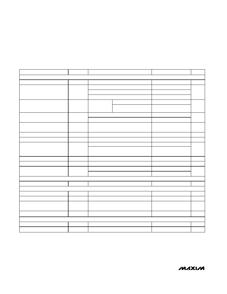
ELECTRICAL CHARACTERISTICS (continued)
(V
DD
= PV
DD
= CPV
DD
= HPV
DD
= 5V, GND = PGND = CPGND = 0V, SHDN = V
DD
, C
BIAS
= 1µF, C1 = C2 = 1µF, speaker load ter-
minated between OUT_+ and OUT_-, headphone load terminated between HPOUT_ and GND, MAX9750: GAIN1 = GAIN2 = VOL =
R
L
= 33k
= GND, MAX9751/MAX9755: GAIN = V
DD
= IN1/2 = GND, T
A
= T
MIN
to T
MAX
, unless otherwise noted. Typical values are
at T
A
= +25∞C.) (Note 1)
PARAMETER
SYMBOL
CONDITIONS
MIN
TYP
MAX
UNITS
HEADPHONE AMPLIFIER (HPS = V
DD
)
Output Offset Voltage
V
OS
T
A
= +25
∞C
±2
±7
mV
HPV
DD
= 3V to 5.5V, T
A
= +25
∞C
70
75
f = 1kHz, V
RIPPLE
= 200mV
P-P
73
Power-Supply Rejection Ratio
(Note 3)
PSRR
f = 10kHz, V
RIPPLE
= 200mV
P-P
63
dB
R
L
= 32
40
50
Output Power
P
OUT
THD+N = 1%,
f = 1kHz,
T
A
= +25
∞C
R
L
= 16
110
mW
R
L
= 32
, P
OUT
= 20mW, f = 1kHz
0.007
Total Harmonic Distortion Plus
Noise
THD+N
R
L
= 16
, P
OUT
= 75mW, f = 1kHz
0.03
%
Signal-to-Noise Ratio
SNR
R
L
= 32
, P
OUT
= 50mW,
BW = 22Hz to 22kHz
95
dB
Noise
V
n
BW = 22Hz to 22kHz
12
µV
RMS
Capacitive-Load Drive
C
L
No sustained oscillations
200
pF
L to R, R to L, f = 10kHz
88
Crosstalk
Any unselected input to any active input,
f = 10kHz (MAX9751)
88
dB
Slew Rate
SR
0.4
V/µs
ESD
ESD
IEC air discharge
±8
kV
GAIN2 = GAIN = 1, GAIN1 = X
0
Gain
A
V
GAIN2 = GAIN = 0, GAIN1 = X
3
dB
CHARGE PUMP
Charge-Pump Frequency
f
OSC
500
550
600
kHz
VOLUME CONTROL (MAX9750_)
VOL Input Impedance
R
VOL
100
M
VOL Input Hysteresis
10
mV
Full Mute Input Voltage
(Note 4)
0.858 x
HPV
DD
V
Channel Matching
A
V
= -25dB to +13.5dB
±0.2
dB
BEEP INPUT (MAX9750_)
Beep Signal Minimum Amplitude
V
BEEP
0.8
V
P-P
Beep Signal Minimum Frequency
f
BEEP
200
Hz
MAX9750/MAX9751/MAX9755
2.6W Stereo Audio Power Amplifiers and
DirectDrive Headphone Amplifiers
_______________________________________________________________________________________
5
ELECTRICAL CHARACTERISTICS (continued)
(V
DD
= PV
DD
= CPV
DD
= HPV
DD
= 5V, GND = PGND = CPGND = 0V, SHDN = V
DD
, C
BIAS
= 1µF, C1 = C2 = 1µF, speaker load ter-
minated between OUT_+ and OUT_-, headphone load terminated between HPOUT_ and GND, MAX9750: GAIN1 = GAIN2 = VOL =
R
L
= 33k
= GND, MAX9751/MAX9755: GAIN = V
DD
= IN1/2 = GND, T
A
= T
MIN
to T
MAX
, unless otherwise noted. Typical values are
at T
A
= +25∞C.) (Note 1)
PARAMETER
SYMBOL
CONDITIONS
MIN
TYP
MAX
UNITS
LOGIC INPUT (
SHDN, GAIN1, GAIN2, GAIN, VOL, IN1/2, HPS)
Logic Input High Voltage
V
IH
2
V
Logic Input Low Voltage
V
IL
0.8
V
Logic Input Current
I
IN
±1
µA
Note 1: All devices are 100% production tested at room temperature. All temperature limits are guaranteed by design.
Note 2: Guaranteed by design. Not production tested.
Note 3: PSRR is specified with the amplifier input connected to GND through C
IN
.
Note 4: See Table 3 for details of the mute levels.
Note 5: The value of R
B
dictates the minimum beep signal amplitude (see the Beep Input section).