
SCOPE: CMOS, BUFFERED, MULTIPLYING 8-BIT D/A CONVERTER
Device Type Generic Number Circuit Function
01
MX7528S(x)/883B DAC with
±
4 LSB
02 MX7528T(x)/883B DAC with
±
2 LSB
03 MX7528U(x)/883B DAC with
±
1 LSB
Case Outline(s). The case outlines shall be designated in Mil-Std-1835 and as follows:
Outline Letter Mil-Std-1835 Case Outline Package Code
MAXIM SMD
Q
R GDIP1-T20 or CDIP2-T20 20 LEAD CERDIP J20
Absolute Maximum Ratings:
V
DD
to AGND ...................................................................................................... 0V, + 17V
V
DD
to DGND ...................................................................................................... 0V, + 17V
V
RFBA
, V
RFBB
to DGND .................................................................................................
±
25V
V
REFA
, V
REFB
to AGND .................................................................................................
±
25V
Digital Input Voltage to DGND .............................................................. -0.3V to V
DD
+0.3V
V pin 1 to DGND .............................................................................................. -0.3V to V
DD
V pin 2, V pin 20 to AGND ..................................................................... -0.3V to V
DD
+0.3V
AGND to DGND ......................................................................................... -0.3V, V
DD
+0.3V
DGND to AGND .......................................................................................................... +0.3V
Lead Temperature (soldering, 10 seconds) ........................................................................ +300
∞
C
Storage Temperature ........................................................................................... -65
∞
C to +150
∞
C
Continuous Power Dissipation ................................................................................... T
A
=
+
70
∞
C
20 pin CERDIP(derate 11.1mW/
∞
C above +70
∞
C) ......................................................... 889mW
Junction Temperature T
J
............................................................................................... +150
∞
C
Thermal Resistance, Junction to Case,
JC
20 pin CERDIP.......................................................................................................... 40
∞
C/W
Thermal Resistance, Junction to Ambient,
JA:
20 pin CERDIP.......................................................................................................... 90
∞
C/W
Recommended Operating Conditions
Ambient Operating Range (T
A
) ..................................................................... -55
∞
C to
+
125
∞
C
Supply Voltage Range (V
DD
) ............................... +4.75V to +5.25V and +14.25V to +15.75V
V
REF
DAC A = V
REF
DAC B ............................................................................................. +10V
OUT DAC A = OUT DAC B ............................................................................................... 0V
Stresses beyond those listed under "Absolute Maximum Ratings" may cause permanent damage to the device.
These are stress ratings only, and functional operation of the device at these or any other conditions beyond
those indicated in the operational sections of the specifications is not implied. Exposure to absolute maximum
rating conditions for extended periods may affect device reliability.
----------------------------
Electrical Characteristics of MX7528/883B
19-0387
Rev. B
for SMD 5962-87701
Page 2 of
7
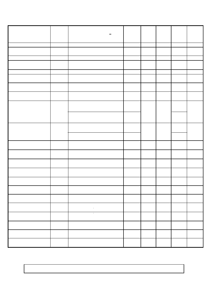
TABLE 1. ELECTRICAL TESTS:
TEST
Symbol
CONDITIONS
-55
∞
C <=T
A
<= +125
∞
C 1/
Unless otherwise specified
Group A
Subgroup
Device
type
Limits
Min
Limits
Max
Units
ACCURACY
Resolution NOTE 4
RES
V
DD
=+5V and V
DD
=+15V
1,2,3
All
8.0
Bits
Relative Accuracy
RA
V
DD
=+5V and V
DD
=+15V
1,2,3
01
±
1.0 LSB
Relative Accuracy
RA
V
DD
=+5V and V
DD
=+15V
1
2,3
02,03
±
1.0
±
0.5
LSB
Relative Accuracy
RA
V
DD
=+5V & V
DD
=+15V, NOTE 2
12
02,03
±
0.5 LSB
Differential Nonlinearity
DNL
V
DD
=+5V and V
DD
=+15V
Monotonic to 8-Bits
1,2,3
All
±
1.0 LSB
Gain Error NOTE 3
AE
V
DD
=+5V and V
DD
=+15V
1
All
±
4.0 LSB
Gain Error NOTE 3
AE
V
DD
=+5V
V
DD
=+15V
2,3
01
±
6.0
±
5.0
LSB
Gain Error NOTE 2,3
AE
V
DD
=+5V
V
DD
=+15V
V
DD
=+5V
V
DD
=+15V
2,3
12
02
±
4.0
±
3.0
±
2.0
±
1.0
LSB
Gain Error NOTE 2,3
AE
V
DD
=+5V
V
DD
=+15V
V
DD
=+5V, V
DD
=+15V
2,3
12
03
±
3.0
±
1.0
±
1.0
LSB
Power Supply Rejection
PSRR
V
DD
=+5V,
V
DD
=
±
5%
1
2,3
All
±
0.02
±
0.04
%/%
Power Supply Rejection
PSRR
V
DD
=+15V,
V
DD
=
±
5%
1
2,3
All
±
0.01
±
0.02
%/%
Output Leakage Current
PIN 2 and 20
I
OL
V
DD
=+5V, DAC latches loaded
with 0000 0000
1
2,3
All
±
50
±
400
nA
Output Leakage Current
PIN 2 and 20
I
OL
V
DD
=+15V, DAC latches loaded
with 0000 0000
1
2,3
All
±
50
±
200
nA
Reference Input
Resistance V
REF
A, V
REF
B
R
IN
V
DD
=+5V and +15V
1,2,3
All
8
15 k
Digital Input High
Voltage
V
IH
V
DD
=+5V
V
DD
=+15V
1,2,3
All
2.4
13.5
V
Digital Input Low
Voltage
V
IL
V
DD
=+5V
V
DD
=+15V
1,2,3
All
0.8
1.5
V
Digital Input Leakage
Current
I
IN
V
DD
=+5V
V
IN
=0V or V
DD
1
2,3
All
±
1.0
±
10
µ
A
Digital Input Leakage
Current
I
IN
V
DD
=+15V
V
IN
=0V or V
DD
1
2,3
All
±
1.0
±
10
µ
A
Supply Current
I
DD
V
DD
=+5V All digital inputs
V
DD
=+15V V
IL
or V
IH
1,2,3
All
2.0
2.0
mA
Supply Current
I
DD
V
DD
=+5V & +15V. All digital
inputs 0V or V
DD
1
2,3
All
100
500
µ
A
Gain Temperature
Coefficient NOTE 4
TC
AE
V
DD
=+5V
V
DD
=+15V
1,2,3
All
±
70
±
35
ppm/
∞
C
----------------------------
Electrical Characteristics of MX7528/883B
19-0387
Rev. B
for SMD 5962-87701
Page 3 of
7

TEST
Symbol
CONDITIONS
-55
∞
C <=T
A
<= +125
∞
C 1/
Unless otherwise specified
Group A
Subgroup
Device
type
Limits
Min
Limits
Max
Units
Feedthrough Error
V
REF
A to OUTA and
V
REF
B to OUTB
FT
REF
A
V
DD
=+5V or V
DD
=+15V,
V
REF
=+10V, 100kHz sinewave,
DAC latches loaded with 0000
0000 NOTE 4, NOTE 5
4,5,6
All
-70 dB
Digital Input
Capacitance
NOTE 6
C
IN
V
DD
=+5V
DB0-DB7
V
DD
=+15V
4
All
10
20
pF
Digital Input
Capacitance
NOTE 6
C
IN
V
DD
=+5V ___ __ _____
WR, CS, DACA/DACB
V
DD
=+15V
4
All
10
15
pF
ANALOG INPUTS
Digital Output pin 2
Capacitance 6/
pin 20
C
OUTA
C
OUTB
V
DD
=+5V and 15V,
DAC latches loaded with 0000
0000
4
All
50
50
pF
Digital Output pin 2
Capacitance 6/
pin 20
C
OUTA
C
OUTB
V
DD
=+5V and 15V,
DAC latches loaded with 1111
1111
4
All
120
120
pF
TIMING
Chip select to write
setup time
NOTE 7
t
CS
V
DD
=+5V
V
DD
=+15V
9
10,11
9
10,11
All
200
230
60
80
ns
Chip select to write
hold time
NOTE 7
t
CH
V
DD
=+5V
V
DD
=+15V
9
10,11
9
10,11
All
20
30
10
15
ns
Write pulse width
NOTE 7
t
WR
V
DD
=+5V, t
CS
t
WR
, t
CH
0
V
DD
=+15V, t
CS
t
WR
, t
CH
0
9
10,11
9
10,11
All
180
200
60
80
ns
Data valid to write
setup time
NOTE 7
t
DS
V
DD
=+5V
V
DD
=+15V
9
10,11
9
10,11
All
110
130
50
70
ns
Data valid to write
hold time
NOTE 7
t
DH
V
DD
=+5V
V
DD
=+15V
9,10,11
All
10
10
ns
Data select to write
setup time
NOTE 7
t
AS
V
DD
=+5V
V
DD
=+15V
9
10,11
9
10,11
All
200
230
60
80
ns
----------------------------
Electrical Characteristics of MX7528/883B
19-0387
Rev. B
for SMD 5962-87701
Page 4 of
7

TEST
Symbol
CONDITIONS
-55
∞
C <=T
A
<= +125
∞
C, 1/
Unless otherwise specified
Group A
Subgroup
Device
type
Limits
Min
Limits
Max
Units
Data select to write
hold time
NOTE 7
t
AH
V
DD
=+5V
V
DD
=+15V
9
10,11
9
10,11
All
20
30
10
15
ns
Reference input
resistance match
RMIN
V
REF
V
DD
=+5V
V
DD
=+15V
4,5,6
All
±
1
±
1
%
Channel to Channel
isolation NOTE 4
V
REF
A to OUTB
CHISO
V
DD
=+5V or +15V. V
REF
A=
±
10V,
100kHz sinewave, V
REF
B=0V
4,5,6
All
-60 dB
Channel to Channel
isolation NOTE 4
V
REF
B to OUTA
CHISO
V
DD
=+5V or +15V. V
REF
B=
±
10V,
100kHz sinewave, DAC,
V
REF
A=0V
4,5,6
All
-60 dB
Output Current
Settling Time
NOTE 4
t
SL
V
DD
=+5V
V
DD
=+15V
9,10,11
All
350
180
ns
NOTE 1: V
OUT
1=0V; VREF=+10V, AGND=DGND unless otherwise specified.
NOTE 2: Optional Subgroup 12 is used for grading and part selection at +25
∞
C.
NOTE 3: Measured using internal RFBA and RFBB. Gain error is adjustable. DAC register loaded with
1111, 1111, 1111.
NOTE 4: Guaranteed, if not tested.
NOTE 5: Feedthrough error can be reduced by connecting the metal lid to ground.
NOTE 6: Subgroup 4 (C
IN
and C
OUT
measurements) shall be measured only for the inital test and after
process or design changes which may affect capacitance.
NOTE 7: Timing in accordance with Write Cycle Timing Diagram in Commercial Data Sheet.
MODE SELECTION TABLE:
__
CS
___
WR
_____
DAC A/DAC B
DAC A
DAC B
L
L
L
Write
Hold
L
L
H
Hold
Write
H
X
X
Hold
Hold
X
H
X
Hold
Hold
L = Low state, H = High state, X = Don't care
TERMINAL CONNECTIONS:
Pin
Pin
1
AGND
11
DB3
2
OUTA
12
DB2
3
RFBA
13
DB1
4
VREFA
14
DB0(LSB)
5
DGND
15
___
CS
6
____
DAC A/DAC B
16
___
WR
7
(MSB)DB7
17
VDD
8
DB6
18
VREFB
9
DB5
19
RFBB
10
DB4
20
OUTB
----------------------------
Electrical Characteristics of MX7528/883B
19-0387
Rev. B
for SMD 5962-87701
Page 5 of
7

ORDERING INFORMATION:
Package
Pkg. Code
Device ID
SMD Number
01
20 pin CERDIP
J20
MX7528SQ/883B
5962-8770101RA
02
20 pin CERDIP
J20
MX7528TQ/883B
5962-8770102RA
03
20 pin CERDIP
J20
MX7528UQ/883B
5962-8770103RA
QUALITY ASSURANCE
Sampling and inspection procedures shall be in accordance with MIL-Prf-38535, Appendix A as specified in Mil-
Std-883.
Screening shall be in accordance with Method 5004 of Mil-Std-883. Burn-in test Method 1015:
1. Test Condition, A, B, C, or D.
2. TA = +125
∞
C minimum.
3. Interim and final electrical test requirements shall be specified in Table 2.
Quality conformance inspection shall be in accordance with Method 5005 of Mil-Std-883, including Groups A, B,
C, and D inspection.
Group A inspection:
1. Tests as specified in Table 2.
2. Selected subgroups in Table 1, Method 5005 of Mil-Std-883 shall be omitted.
Group C and D inspections:
a. End-point electrical parameters shall be specified in Table 1.
b. Steady-state life test, Method 1005 of Mil-Std-883:
1. Test condition A, B, C, D.
2. TA = +125
∞
C, minimum.
3. Test duration, 1000 hours, except as permitted by Method 1005 of Mil-Std-883.
TABLE 2. ELECTRICAL TEST REQUIREMENTS
Mil-Std-883 Test Requirements
Subgroups
per Method 5005, Table 1
Interim Electric Parameters
Method 5004
1
Final Electrical Parameters
Method 5005
1*, 2, 3, 12
Group A Test Requirements
Method 5005
1, 2, 3, 4, 5, 6, 9, 10**, 11**, 12
Group C and D End-Point Electrical Parameters
Method 5005
1
* PDA applies to Subgroup 1 only.
** Subgroups 10 and 11, if not tested shall be guaranteed to the limits specified in Table 1.
----------------------------
Electrical Characteristics of MX7528/883B
19-0387
Rev. B
for SMD 5962-87701
Page 6 of
7