 | –≠–ª–µ–∫—Ç—Ä–æ–Ω–Ω—ã–π –∫–æ–º–ø–æ–Ω–µ–Ω—Ç: MX7534BQ | –°–∫–∞—á–∞—Ç—å:  PDF PDF  ZIP ZIP |
_______________General Description
The MX7534/MX7535 are high-performance, CMOS,
monolithic, 14-bit digital-to-analog converters (DACs).
Wafer-level, laser-trimmed, thin-film resistors and tempera-
ture-compensated NMOS switches assure operation over
the full operating temperature range with exceptional lin-
ear and gain stability.
The MX7534 accepts right-justified data in two bytes from
an 8-bit bus, while the MX7535 operates with a 14-bit data
bus with separate MS-byte and LS-byte select controls. In
addition, all digital inputs are compatible with both TTL and
5V CMOS-logic levels. The MX7534/MX7535 are intended
for unipolar operation, but may be operated as bipolar
DACs with additional external components. Both devices
are protected against CMOS latchup, and neither requires
the use of external Schottky protection diodes.
The MX7534 is available in 20-pin narrow (0.3") DIP, wide
SO, or PLCC packages. The MX7535 is available in
28-pin, 600 mil wide DIP, wide SO, or PLCC packages.
________________________Applications
Machine and Motion Control Systems
Automatic Test Equipment
Digital Audio
µP-Controlled Calibration Circuitry
Programmable-Gain Amplifiers
Digitally Controlled Filters
Programmable Power Supplies
____________________________Features
o
14-Bit Monotonic Over Full Temperature Range
o
Full 4-Quadrant Multiplication
o
µP-Compatible, Double-Buffered Inputs
o
Exceptionally Low Gain Tempco (2.5ppm/∞C)
o
Low Output Leakage (<20nA) Over Temp.
o
Low Power Consumption
o
TTL and CMOS Compatible
______________Ordering Information
Ordering Information continued at end of data sheet.
*
Dice are tested at +25∞C, DC parameters only.
MX7534/MX7535
Microprocessor-Compatible,
14-Bit DACs
________________________________________________________________
Maxim Integrated Products
1
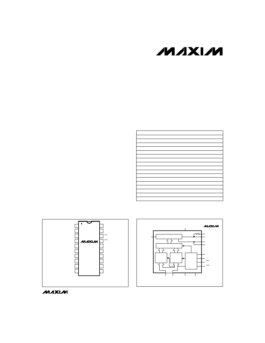
MX7534
DAC REGISTER
MS
INPUT
REGISTER
LS
INPUT
REGISTER
14
6
8
2
3
4
5
15
16
18
17
20
6
7≠14
19
14-BIT DAC
CONTROL
LOGIC
1
REF
RFB
IOUT
AGNDS
AGNOF
A1
A0
CS
WR
V
DD
D7≠D0
DGND
V
SS
Functional diagrams continued at end of data sheet.
_______________Functional Diagrams
_________________Pin Configurations
19-1116; Rev 1; 11/96
For free samples & the latest literature: http://www.maxim-ic.com, or phone 1-800-998-8800
PART
TEMP. RANGE
PIN-PACKAGE INL (LSBs)
MX7534
KN
0∞C to +70∞C
20 Plastic DIP
±1
MX7534JN
0∞C to +70∞C
20 Plastic DIP
±2
MX7534KCWP
0∞C to +70∞C
20 SO
±1
MX7534JCWP
0∞C to +70∞C
20 SO
±2
MX7534KP
0∞C to +70∞C
20 PLCC
±1
MX7534JP
0∞C to +70∞C
20 PLCC
±2
MX7534J/D
0∞C to +70∞C
Dice*
±2
MX7534BQ
-25∞C to +85∞C
20 CERDIP
±1
MX7534AQ
-25∞C to +85∞C
20 CERDIP
±2
MX7534BD
-25∞C to +85∞C
20 Ceramic SB
±1
MX7534AD
-25∞C to +85∞C
20 Ceramic SB
±2
MX7534KEWP
-40∞C to +85∞C
20 SO
±1
MX7534JEWP
-40∞C to +85∞C
20 SO
±2
MX7534TQ
-55∞C to +125∞C
20 CERDIP
±1
MX7534SQ
-55∞C to +125∞C
20 CERDIP
±2
MX7534TD
-55∞C to +125∞C
20 Ceramic SB
±1
MX7534SD
-55∞C to +125∞C
20 Ceramic SB
±2
20
19
18
17
16
15
14
13
1
2
3
4
5
6
7
8
V
SS
V
DD
CS
WR
AGNDS
IOUT
RFB
REF
TOP VIEW
A0
A1
D0
D1
D6
D7
DGND
AGNDF
12
11
9
10
D2
D3
D4
MX7535 at end of data sheet.
D5
DIP/SO/PLCC/Ceramic SB
MX7534

MX7534/MX7535
Microprocessor-Compatible,
14-Bit DACs
2
_______________________________________________________________________________________
ABSOLUTE MAXIMUM RATINGS
ELECTRICAL CHARACTERISTICS
(V
DD
= +11.4V to +15.75V (Note 1), V
REF
= 10V, V
IOUT
= V
AGNDS
= V
SS
= 0V, T
A
= T
MIN
to T
MAX
, unless otherwise noted.)
Stresses beyond those listed under "Absolute Maximum Ratings" may cause permanent damage to the device. These are stress ratings only, and functional
operation of the device at these or any other conditions beyond those indicated in the operational sections of the specifications is not implied. Exposure to
absolute maximum rating conditions for extended periods may affect device reliability.
V
DD
to DGND ............................................................-0.3V, +17V
V
SS
to AGND .............................................................-15V, +0.3V
REF to AGND (MX7534) ......................................................±25V
REFS to AGND (MX7535) ....................................................±25V
REFF to AGND (MX7535) ....................................................±25V
RFB to AGND.......................................................................±25V
Digital Input Voltage to DGND.........................-0.3V, V
DD
+ 0.3V
IOUT to DGND .................................................-0.3V, V
DD
+ 0.3V
AGND to DGND ...............................................-0.3V, V
DD
+ 0.3V
Continuous Power Dissipation (T
A
= +70∞C)
20-Pin Plastic DIP (derate 11.11mW/∞C above +70∞C)....889mW
28-Pin Plastic DIP (derate 14.29mW/∞C above +70∞C) ......1.14W
20-Pin SO (derate 10.00mW/∞C above +70∞C)..............800mW
28-Pin SO (derate 12.50mW/∞C above +70∞C).....................1W
20-Pin PLCC (derate 10.00mW/∞C above +70∞C) .........800mW
28-Pin PLCC (derate 10.53mW/∞C above +70∞C) .........842mW
20-Pin CERDIP (derate 11.11mW/∞C above +70∞C)......889mW
28-Pin CERDIP (derate 16.67mW/∞C above +70∞C)........1.33W
20-Pin Ceramic SB
(derate 11.76mW/∞C above +70∞C) .............................941mW
28-Pin Ceramic SB
(derate 20.00mW/∞C above +70∞C) ................................1.6W
Operating Temperature Ranges
MX753_J/K ............................................................0∞C to +70∞C
MX753_A/B ........................................................-25∞C to +85∞C
MX753_EW_.......................................................-40∞C to +85∞C
MX753_S/T.......................................................-55∞C to +125∞C
Storage Temperature Range .............................-65∞C to +150∞C
Lead Temperature (soldering, 10sec) .............................+300∞C
±10
Input Leakage Current
µA
±1
V
INL
Input Low Voltage
V
0.8
V
2.4
V
INH
Input High Voltage
k
3.5
6
10
R
REF
Reference Voltage Input
Resistance (Note 3)
nA
±150
I
OUT
Output Leakage Current
±1
Bits
14
Resolution
±25
±5
ppm/∞C
±0.5
±5
Gain Temperature Coefficient
(Note 2)
±0.5
±2.5
LSB
±2
INL
Relative Accuracy
±4
LSB
±8
Full-Scale Error
UNITS
MIN
TYP
MAX
SYMBOL
PARAMETER
MX753_K/B/T
T
A
= T
MIN
to T
MAX
MX753_J/K/A/B
MX753_J/A/S
Measured with internal R
FB
,
includes effects of leakage
current and gain TC
MX753_S/T
CONDITIONS
LSB
±1
Guaranteed Monotonic
Differential Nonlinearity
pF
7
C
IN
Input Capacitance (Note 2)
T
A
= T
MIN
to T
MAX
All digital
inputs at 0V
All digital
inputs at 0V,
V
SS
= 0V
T
A
= +25∞C
MX753_J/A/S
MX753_K/B/T
MX753_J/A/S
MX753_K/B/T
T
A
= +25∞C
Digital inputs
at 0V or V
DD
DC ACCURACY
REFERENCE INPUT
DIGITAL INPUTS

MX7534/MX7535
Microprocessor-Compatible,
14-Bit DACs
_______________________________________________________________________________________
3
mV
-200
-500
V
SS
Negative Supply-Voltage Range
V
11.4
15.75
V
DD
Positive Supply-Voltage Range
mA
3
4
I
DD
Positive Supply Current
µA
500
I
SS
Negative Supply Current
UNITS
MIN
TYP
MAX
SYMBOL
PARAMETER
For specific performance
For specific performance
MX7534
MX7535
Digital inputs at 0V or V
DD
CONDITIONS
Digital inputs at
V
INH
or V
INL
ELECTRICAL CHARACTERISTICS (continued)
(V
DD
= +11.4V to +15.75V (Note 1), V
REF
= 10V, V
IOUT
= V
AGNDS
= V
SS
= 0V, T
A
= T
MIN
to T
MAX
, unless otherwise noted.)
mVp-p
3
nV-sec
50
µs
0.8
1.5
Output Current Setting Time
Digital-to-Analog Glitch Impulse
nV/Hz
15
Output Noise Voltage Density
(10Hz≠100kHz)
130
C
OUT
Output Capacitance (IOUT Pin)
5
Multiplying Feedthrough Error
(Note 5)
%/%
±0.01
±0.02
Power-Supply Rejection
pF
260
UNITS
MIN
TYP
MAX
SYMBOL
PARAMETER
T
A
= +25∞C
Measured with V
REF
= 0V,
IOUT loads = 100
II
13pF, DAC register
alternately loaded with all 1s and all 0s
T
A
= +25∞C, to 0.003% of full-scale range,
IOUT load = 100
II
13pF, DAC register
alternately loaded with all 1s and all 0s
Measured between R
FB
and I
OUT
DAC register loaded with all 0s
T
A
= T
MIN
to T
MAX
T
A
= +25∞C
T
A
= T
MIN
to T
MAX
DAC register loaded with all 1s
CONDITIONS
V
REF
= ±10V, 10kHz
sine wave, DAC register
loaded with all 0s
V
DD
= ±5%
Note 1:
Specifications are guaranteed for V
DD
of +11.4V to +15.75V. At V
DD
= +5V, device is still functional with degraded specifications.
Note 2:
Guaranteed by design, not tested.
Note 3:
Resistors have a typical -300ppm/∞C tempco.
AC PERFORMANCE CHARACTERISTICS
(Note 4)
(V
DD
= +11.4V to +15.75V, V
REF
= 10V, V
IOUT
= V
AGND
(V
AGNDS
for MX7535) = V
SS
= 0V, output amplifier is AD544*,
T
A
= T
MIN
to T
MAX
, unless otherwise noted.)
Note 4:
These characteristics are included for design guidance only, and are not subject to test.
Note 5:
Feedthrough can be further reduced by connecting the metal lid on the ceramic package to DGND.
* AD544 is an Analog Devices part.
POWER REQUIREMENTS

MX7534/MX7535
Microprocessor-Compatible,
14-Bit DACs
4
_______________________________________________________________________________________
TIMING CHARACTERISTICS (MX7534)
(V
DD
= +11.4V to +15.75V, V
REF
= 10V, V
IOUT
= V
AGND
= V
SS
= 0V, T
A
= T
MIN
to T
MAX
, unless otherwise noted. See Figure 1a for
timing diagram.)
ns
170
ns
0
t
2
ns
0
t
1
CSMSB or CSLSB to WR Setup Time
CSMSB or CSLSB to WR Hold Time
240
t
4
Write Pulse Width
200
240
t
3
LDAC Pulse Width
ns
170
200
UNITS
MIN
TYP
MAX
SYMBOL
PARAMETER
T
A
= +25∞C
T
A
= -55∞C to +125∞C
T
A
= -25∞C to +85∞C
T
A
= -55∞C to +125∞C
T
A
= +25∞C
T
A
= -25∞C to +85∞C
CONDITIONS
ns
140
30
t
6
Data-Hold Time
160
180
t
5
Data-Setup Time
ns
20
20
T
A
= +25∞C
T
A
= -55∞C to +125∞C
T
A
= -25∞C to +85∞C
T
A
= -55∞C to +125∞C
T
A
= +25∞C
T
A
= -25∞C to +85∞C
TIMING CHARACTERISTICS (MX7535)
(V
DD
= +11.4V to +15.75V, V
REF
= 10V, V
IOUT
= V
AGNDS
= V
SS
= 0V, T
A
= T
MIN
to T
MAX
, unless otherwise noted. See Figure 1b for
timing diagram.)
ns
60
ns
0
t
2
ns
0
t
1
Address Valid to Write Setup Time
Address Valid to Write Hold Time
30
t
4
Data Hold Time
70
80
t
3
Data Setup Time
ns
20
20
UNITS
MIN
TYP
MAX
SYMBOL
PARAMETER
T
A
= +25∞C
T
A
= -55∞C to +125∞C
T
A
= -25∞C to +85∞C
T
A
= -55∞C to +125∞C
T
A
= +25∞C
T
A
= -25∞C to +85∞C
CONDITIONS
240
t
7
Write Pulse Width
0
0
ns
170
200
T
A
= -55∞C to +125∞C
T
A
= +25∞C
T
A
= -25∞C to +85∞C
ns
ns
t
6
t
5
Chip-Select to Write-Hold Time
Chip-Select to Write-Setup Time

MX7534/MX7535
Microprocessor-Compatible,
14-Bit DACs
_______________________________________________________________________________________
5
__________Pin Description (MX7534)
NAME
FUNCTION
1
REF
Reference Input to DAC
2
RFB
PIN
3
IOUT
Current Output
4
AGNDS
Analog Ground Sense. Reference
point for external circuitry. AGNDS
should carry minimum current.
8
D6
Data Bit 6
7
D7
Data Bit 7
6
DGND
Digital Ground
5
AGNDF
Analog Ground Force. Carries current
from internal analog ground connec-
tions. AGNDS and AGNDF are tied
together internally.
Feedback Resistor. Used to close the
loop around an external op amp.
__________Pin Description (MX7535)
NAME
FUNCTION
1
REFS
Reference Voltage Sense
2
REFF
4
PIN
3
RFB
Feedback Resistor. Used to close the
loop around an external op amp.
5
AGNDS
Analog Ground Sense. Reference
point for external circuitry. This pin
should carry minimum current.
9
D12
Data Bit 12
8
D13
Data Bit 13 (MSB)
7
DGND
Digital Ground
6
AGNDF
Analog Ground Force. Carries current
from internal analog ground
connections. AGNDS and AGNDF
are tied together internally.
IOUT
Current Output
11
D10
Data Bit 10
10
D11
Data Bit 11
13
D8
Data Bit 8
12
D9
Data Bit 9
Reference Voltage Force
11
D3
Data Bit 3 or Data Bit 11
10
D4
Data Bit 4 or Data Bit 12
9
D5
Data Bit 5 or Data Bit 13 (MSB)
14
D0
Data Bit 0 (LSB) or Data Bit 8
13
D1
Data Bit 1 or Data Bit 9
12
D2
Data Bit 2 or Data Bit 10
17
WR
Write Input. Active low.
16
A0
Address Input 0
15
A1
Address Input 1
20
V
SS
Bias pin for high-temperature,
low-leakage configuration
19
V
DD
+12V to +15V Supply-Voltage Input
18
CS
Chip-Select Input. Active low.
14
D7
Data Bit 7
15
D6
Data Bit 6
16
D5
Data Bit 5
20
D1
Data Bit 1
17
D4
Data Bit 4
18
D3
Data Bit 3
19
D2
Data Bit 2
21
D0
Data Bit 0 (LSB)
22
CSMSB
Chip-Select Most Significant Byte.
Active low.
23
LDAC
Asynchronous Load DAC Input.
Active low.
24
CSLSB
Chip-Select Least Significant Byte.
Active low.
25
WR
Write Input. Active low.
28
N.C.
No Connection. Not internally connected.
26
V
DD
+12V to +15V Supply-Voltage Input
27
V
SS
Bias pin for high-temperature,
low-leakage configuration