
General Description
The MXL1543 is a three-driver/three-receiver multipro-
tocol transceiver that operates from a +5V single sup-
ply. The MXL1543, along with the MXL1544/MAX3175
and the MXL1344A, form a complete software-selec-
table data terminal equipment (DTE) or data communi-
cation equipment (DCE) interface port that supports the
V.28 (RS-232), V.10/V.11 (RS-449/V.36, EIA-530, EIA-
530A, X.21), and V.35 protocols. The MXL1543 trans-
ceivers carry the high-speed clock and data signals
while the MXL1544/MAX3175 carry the control signals.
The MXL1543 can be terminated by the MXL1344A
software-selectable resistor termination network or by
discrete termination networks.
An internal charge pump and a proprietary low-dropout
transmitter output stage allow V.11- , V.28- , and V.35-
compliant operation from a +5V single supply. A no-
cable mode is entered when all mode pins (M0, M1,
and M2) are pulled high or left unconnected. In no-
cable mode, supply current decreases to 0.5µA and all
transmitter and receiver outputs are disabled (high
impedance). Short-circuit current limiting and thermal
shutdown circuitry protect the drivers against excessive
power dissipation.
Applications
Features
o MXL1543, MXL1544/MAX3175, and MXL1344A
Chipset Is Pin Compatible with LTC1543,
LTC1544, and LTC1344A
o Supports RS-232, RS-449, EIA-530, EIA-530A,
V.35, V.36, and X.21
o Software-Selectable Cable Termination Using the
MXL1344A
o Complete DTE or DCE Port with MXL1544/
MAX3175, and MXL1344A
o +5V Single-Supply Operation
o 0.5µA No-Cable Mode
o TUV-Certified NET1/NET2 and TBR1/TBR2-
Compliant
MXL1543
+5V Multiprotocol, 3Tx/3Rx, Software-
Selectable Clock/Data Transceivers
________________________________________________________________ Maxim Integrated Products
1
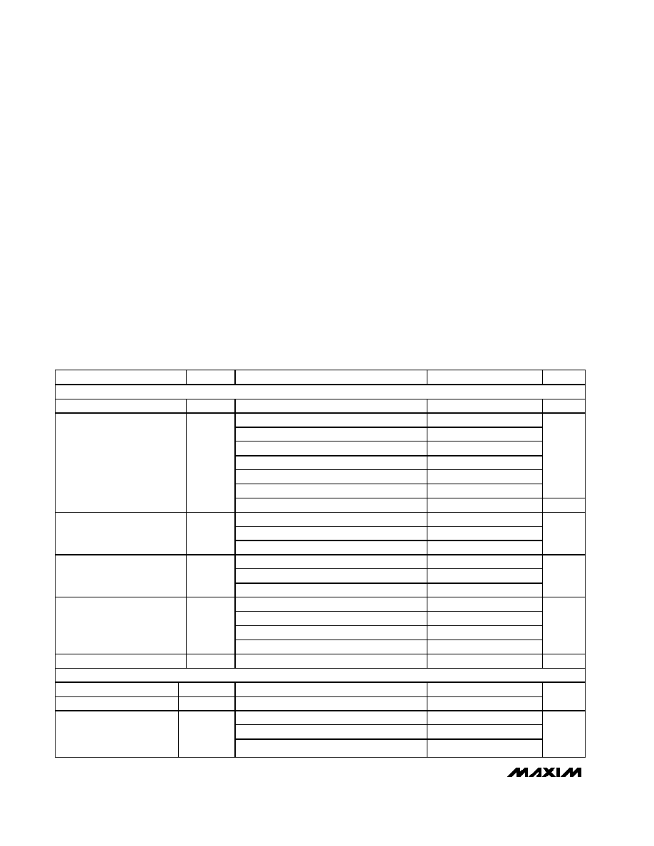
Ordering Information
19-1929; Rev 1; 9/01
PART
TEMP. RANGE
PIN-PACKAGE
MXL1543CAI
0
∞ to +70∞C
28 SSOP
Data Networking
CSU and DSU
Data Routers
PCI Cards
Telecommunications
Equipment
Typical Operating Circuit
D1
D2
D3
D4
R1
R2
R3
MXL1543
RXD
RXC
TXD
TXC
SCTE
D1
D2
D3
R1
R2
R3
MXL1544
MAX3175
CTS
DSR
RTS
DTR
DCD
RXC B
RXD A (104)
RXD B
SG (102)
SHIELD (101)
RTS A (105)
RTS B
DTR A (108)
DTR B
DCD A (107)
DCD B
DSR A (109)
CTS A (106)
DSR B
CTS B
LL A (141)
TXD B
SCTE A (113)
SCTE B
TXC A (114)
TXC B
TXD A (103)
DB-25 CONNECTOR
13
R4
LL
RXC A (115)
18
5
10 8
22 6
23 20 19 4
1
7
16 3
9 17
12 15 11 24 14 2
MXL1344A
Pin Configuration appears at end of data sheet.
For pricing, delivery, and ordering information, please contact Maxim/Dallas Direct! at
1-888-629-4642, or visit Maxim's website at www.maxim-ic.com.
MXL1543
+5V Multiprotocol, 3Tx/3Rx, Software-
Selectable Clock/Data Transceivers
2
_______________________________________________________________________________________
ABSOLUTE MAXIMUM RATINGS
ELECTRICAL CHARACTERISTICS
(V
CC
= +5.0V, C1 = C2 = C4 = 1µF, C3 = C5 = 4.7µF, (Figure 10), T
A
= T
MIN
to T
MAX
. Typical values are at T
A
= +25∞C, unless oth-
erwise noted.)
Stresses beyond those listed under "Absolute Maximum Ratings" may cause permanent damage to the device. These are stress ratings only, and functional
operation of the device at these or any other conditions beyond those indicated in the operational sections of the specifications is not implied. Exposure to
absolute maximum rating conditions for extended periods may affect device reliability.
All Voltages Referenced to GND Unless Otherwise Noted.
Supply Voltages
V
CC
.......................................................................-0.3V to +6V
V
DD
....................................................................-0.3V to +7.3V
V
EE
.....................................................................+0.3V to -6.5V
V
DD
to V
EE
(Note 1) ................................................................13V
Logic Input Voltages
M0, M1, M2, DCE/DTE, T_IN ................................-0.3V to +6V
Logic Output Voltages
R_OUT ....................................................-0.3V to (V
CC
+ 0.3V)
Transmitter Outputs
T_OUT_, T3OUT_/R1IN_.....................................-15V to +15V
Short-Circuit Duration............................................Continuous
Receiver Input
R_IN_T3OUT_/R1IN_ ..........................................-15V to +15V
Continuous Power Dissipation (T
A
= +70∞C)
28-Pin SSOP (derate 11.1mW/∞C above +70∞C) .........889mW
Operating Temperature Range
MXL1543CAI .......................................................0∞C to 70∞C
Junction Temperature .......................................................150∞C
Storage Temperature Range ...........................-65∞C to +150∞C
Lead Temperature (soldering, 10s) ...............................+300∞C
PARAMETER
SYMBOL
CONDITIONS
MIN
TYP
MAX
UNITS
DC CHARACTERISTICS
V
CC
Operating Range
V
CC
4.75
5.25
V
RS-530, RS-530A, X.21, no load
13
RS-530, RS-530A, X.21, full load
100
130
V.35 mode, no load
20
V.35 mode, full load
126
170
V.28 mode, no load
20
V.28 mode, full load
40
75
mA
Supply Current
(DCE Mode)
(Digital Inputs = GND or
V
CC
)
(Transmitter Outputs Static)
I
CC
No-cable mode
0.5
10
µA
RS-530, RS-530A, X.21, full load
230
V.35 mode, full load
600
Internal Power Dissipation
(DCE Mode)
P
D
V.28 mode, full load
140
mW
Any mode (except no-cable mode), no load
6.4
6.8
V.28 mode, with load
6.4
6.8
Positive Charge-Pump
Output Voltage
V
DD
V.28, V.35 modes, with load, I
DD
= 10mA
6.4
6.8
V
V.28, V.35, no load
-5.6
V.28 mode, full load
-5.6
-5.4
V.35 mode, full load
-5.6
-5.4
Negative Charge-Pump
Output Voltage
V
EE
RS-530, RS-530A, X.21, full load
-5.6
-5.4
V
Supply Rise Time
t
r
No-cable mode or power-up to turn on
500
µs
LOGIC INPUTS (M0, M1, M2, DCE/DTE, T1IN, T2IN, T3IN)
Input High Voltage
V
IH
2.0
Input Low Voltage
V
IL
0.8
V
T1IN, T2IN, T3IN
±10
M0, M1, M2, DCE/DTE = GND
-100
-50
-30
Logic Input Current
I
IN
M0, M1, M2, DCE/DTE = V
CC
±10
µA
Note 1: V
DD
and V
EE
absolute difference cannot exceed 13V.

MXL1543
+5V Multiprotocol, 3Tx/3Rx, Software-
Selectable Clock/Data Transceivers
_______________________________________________________________________________________
3
ELECTRICAL CHARACTERISTICS (continued)
(V
CC
= +5.0V, C1 = C2 = C4 = 1µF, C3 = C5 = 4.7µF, (Figure 10), T
A
= T
MIN
to T
MAX
. Typical values are at T
A
= +25∞C, unless oth-
erwise noted.)
PARAMETER
SYMBOL
CONDITIONS
MIN
TYP
MAX
UNITS
LOGIC OUTPUTS (R1OUT, R2OUT, R3OUT)
Output High Voltage
V
OH
I
SOURCE
= 4mA
3
4.5
Output Low Voltage
V
OL
I
SINK
= 4mA
0.3
0.8
V
Output Short-Circuit Current
I
SC
0
V
OUT
V
CC
±50
mA
Output Pullup Current
I
L
V
OUT
= 0, no-cable mode
70
µA
V.11 TRANSMITTER
Open-Circuit Differential Output
Voltage
V
ODO
Open circuit, R = 1.95k
(Figure 1)
±5
V
R = 50
(Figure 1), T
A
= +25
o
C
0.5
V
ODO
0.67
V
ODO
Loaded Differential Output
Voltage
V
ODL
R = 50
(Figure 1)
±2
V
Change in Magnitude of Output
Differential Voltage
V
OD
R = 50
(Figure 1)
0.2
V
Common-Mode Output Voltage
V
OC
R = 50
(Figure 1)
3.0
V
Change in Magnitude of Output
Common-Mode Voltage
V
OC
R = 50
(Figure 1)
0.2
V
Short-Circuit Current
I
SC
V
OUT
= GND
150
mA
Output Leakage Current
I
Z
-0.25V
V
OUT
+0.25V, power-off or
no-cable mode
±1
±100
µA
Rise or Fall Time
t
r,
t
f
(Figures 2, 6)
2
10
25
ns
Transmitter Input to Output
Delay
t
PHL
,
t
PLH
(Figures 2, 6)
40
80
ns
Data Skew
ItPHL- tPLHI
(Figures 2, 6)
3
12
ns
Output to Output Skew
tSKEW
(Figures 2, 6)
3
ns
V.11 RECEIVER
Differential Threshold Voltage
V
TH
-7V
V
CM
7V
-200
200
mV
Input Hysteresis
V
TH
-7V
V
CM
7V
15
40
mV
Receiver Input Current
I
IN
-10V
V
A,
B
10V
±0.66
mA
Receiver Input Resistance
R
IN
-10V
V
A,
B
10V
15
30
k
Rise or Fall Time
t
r
,
t
f
(Figures 2, 7)
15
ns
Receiver Input to Output Delay
t
PHL
,t
PLH
(Figures 2, 7)
50
80
ns
Data Skew
|tPHL- tPLH|
(Figures 2, 7)
4
16
ns
V.35 TRANSMITTER
Open circuit (Figure 3)
±7
Differential Output Voltage
V
OD
With load, -4V
V
CM
4V (Figure 3)
±0.44
±0.55
±0.66
V
Output High Current
I
OH
V
A,B
= 0
-13
-11
-9
mA
Output Low Current
I
OL
V
A,B
= 0
9
11
13
mA
MXL1543
+5V Multiprotocol, 3Tx/3Rx, Software-
Selectable Clock/Data Transceivers
4
_______________________________________________________________________________________
PARAMETER
SYMBOL
CONDITIONS
MIN
TYP
MAX
UNITS
Output Leakage Current
I
Z
-0.25V
V
OUT
+0.25V, power-off or no-
cable mode
±1
±100
µA
Rise or Fall Time
t
r
, t
f
(Figures 3, 6)
5
ns
Transmitter Input to Output
Delay
t
PHL
,
t
PLH
(Figures 3, 6)
35
80
ns
Data Skew
|tPHL≠tPLH|
(Figures 3, 6)
4
16
ns
Output-to-Output Skew
t
SKEW
(Figures 3, 6)
4
ns
V.35 RECEIVER
Differential Input Voltage
V
TH
-2V
V
CM
2V (Figure 3)
-200
200
mV
Input Hysteresis
V
TH
-2V
V
CM
2V (Figure 3)
15
40
mV
Receiver Input Current
I
IN
-10V
V
A
,
B
10V
±0.66
mA
Receiver Input Resistance
R
IN
-10V
V
A
,
B
10V
15
30
k
Rise or Fall Time
t
r
, t
f
(Figures 3, 7)
15
ns
Receiver Input to Output Delay
tPHL, tPLH
(Figures 3, 7)
50
80
ns
Data Skew
|tPHL≠tPLH|
(Figures 3, 7)
4
16
ns
V.28 TRANSMITTER
Open circuit
±7
Output Voltage Swing (Figure 4)
V
O
R
L
= 3k
±5
±6
V
Short-Circuit Current
I
SC
±150
mA
Output Leakage Current
I
Z
-0.25V
V
OUT
+0.25V, power-off or no-
cable mode
±1
±100
µA
Output Slew Rate
SR
R
L
= 3k
, C
L
= 2500pF (Figures 4, 8)
4
30
V/
µs
Transmitter Input to Output
Delay
t
PHL
R
L
= 3k
, C
L
= 2500pF (Figures 4, 8)
1.5
2.5
µs
Transmitter Input to Output
Delay
t
PLH
R
L
= 3k
, C
L
= 2500pF (Figures 4, 8)
1.5
3
µs
V.28 RECEIVER
Input Threshold Low
V
IL
0.8
1.2
V
Input Threshold High
V
IH
1.2
2.0
V
Input Hysteresis
V
HYST
0.05
0.3
V
Input Resistance
R
IN
-15V
V
IN
+15V
3
5
7
k
Rise or Fall Time
t
r
, t
f
(Figures 5, 9)
15
ns
Receiver Input to Output Delay
t
PHL
(Figures 5, 9)
60
100
ns
Receiver Input to Output Delay
t
PLH
(Figures 5, 9)
160
250
ns
ELECTRICAL CHARACTERISTICS (continued)
(V
CC
= +5.0V, C1 = C2 = C4 = 1µF, C3 = C5 = 4.7µF, (Figure 10), T
A
= T
MIN
to T
MAX
. Typical values are at T
A
= +25∞C, unless oth-
erwise noted.)

MXL1543
+5V Multiprotocol, 3Tx/3Rx, Software-
Selectable Clock/Data Transceivers
_______________________________________________________________________________________
5
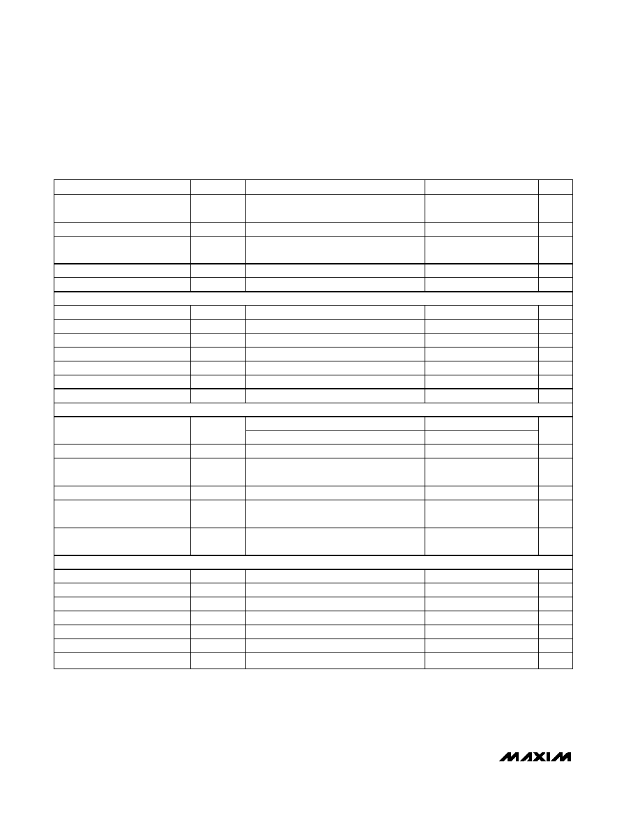
160
0
0.1
100
1000
V.11 SUPPLY CURRENT
vs. DATA RATE
40
20
60
80
100
120
140
MXL1543 toc01
DATA RATE (kbps)
SUPPLY CURRENT (mA)
10
1
10,000
DCE MODE, R = 50
, ALL TRANSMITTERS
OPERATING AT THE SPECIFIED DATA RATE
0
20
60
40
80
100
0
100
50
150
200
250
V.28 SUPPLY CURRENT
vs. DATA RATE
MXL1543 toc02
DATA RATE (kbps)
SUPPLY CURRENT (mA)
DCE MODE ALL TRANSMITTERS
OPERATING AT THE SPECIFIED DATA RATE
R
L
= 3k
, C
L
= 2500pF
160
0
0.1
100
1000
V.35 SUPPLY CURRENT
vs. DATA RATE
40
20
60
80
100
120
140
MXL1543 toc03
DATA RATE (kbps)
SUPPLY CURRENT (mA)
10
0.1
10,000
DCE MODE, FULL LOAD, ALL TRANSMITTERS
OPERATING AT THE SPECIFIED DATA RATE
180
200
-5
-2
-3
-4
0
-1
4
3
2
1
5
0
10
20
30
40
50
60
70
V.11 DRIVER DIFFERENTIAL OUTPUT
VOLTAGE vs. TEMPERATURE
MXL1543 toc04
TEMPERATURE (
∞C)
DRIVER DIFFERENTIAL OUTPUT VOLTAGE (V)
DCE MODE, R = 50
V
OUT+
V
OUT-
8
V.28 OUTPUT VOLTAGE
vs. TEMPERATURE
MXL1543 toc05
TEMPERATURE (
∞C)
OUTPUT VOLTAGE (V)
0
30
40
10
20
50
60
70
10
4
6
0
2
-4
-2
-8
-6
-10
DCE MODE, R
L
= 3k
V
OUT+
V
OUT-
-0.66
-0.22
-0.44
0.22
0
0.44
0.66
0
30
40
10
20
50
60
70
OUTPUT VOLTAGE (V)
V.35 OUTPUT VOLTAGE
vs. TEMPERATURE
MXL1543 toc06
TEMPERATURE (
∞C)
DCE MODE, V
CM
= 0
FULL LOAD
V
OL
V
OH
520
540
530
560
550
570
580
590
600
-4
-2
-1
-3
0
1
2
3
4
V.35 DIFFERENTIAL OUTPUT VOLTAGE
vs. COMMON-MODE VOLTAGE
MXL1543 toc07
COMMON-MODE VOLTAGE (V)
DIFFERENTIAL OUTPUT VOLTAGE (mV)
|V
OD
|
-300
0
-100
-200
100
200
300
-10
-2
-4
-8
-6
0
2
4
6
8
10
V.11/V.35 RECEIVER INPUT CURRENT
vs. INPUT VOLTAGE
MXL1543 toc08
INPUT VOLTAGE (V)
RECEIVER INPUT CURRENT (µ
A
)
DCE MODE
-0.5
1.0
0.5
0
1.5
2.0
2.5
-10
-2
-4
-8
-6
0
2
4
6
8
10
V.28 RECEIVER INPUT CURRENT
vs. INPUT VOLTAGE
MXL1543 toc09
INPUT VOLTAGE (V)
RECEIVER INPUT CURRENT (mA)
DCE MODE
-2.0
-2.5
-1.5
-1.0
Typical Operating Characteristics
(V
CC
= +5.0V, C1 = C2 = C4 =1µF, C3 = C5 = 4.7µF, (Figure 10), T
A
= T
MIN
to T
MAX
, T
A
= +25∞C, unless otherwise noted.)