 | –≠–ª–µ–∫—Ç—Ä–æ–Ω–Ω—ã–π –∫–æ–º–ø–æ–Ω–µ–Ω—Ç: REF01CSA | –°–∫–∞—á–∞—Ç—å:  PDF PDF  ZIP ZIP |
General Description
The REF01 and REF02 are precision voltage references
that are pretrimmed to within ±3% of +10V and +5V,
respectively. Both references feature excellent tempera-
ture stability (as low as 8.5 ppm/∞C worst case), low cur-
rent drain, and low noise. The REF02 also provides a
TEMP pin whose output voltage varies linearly with tem-
perature, making this device suitable for a wide variety of
temperature-sensing and control applications. Both
devices are available from Maxim in the space-saving SO
package, as well as in the standard 8-pin TO-99 and
MINI-DIP packages.
Features
o Pretrimmed to +5V, +10V ±0.3%
o Excellent Temperature Stability: 3ppm/∞C
o Low Noise: 10µVp-p (REF02)
o Low Supply Current: 1.4mA max
o Short-Circuit Proof
o Linear Temperature Transducer O/P (REF02)
REF01/REF02
+5V, +10V Precision
Voltage References
________________________________________________________________ Maxim Integrated Products
1
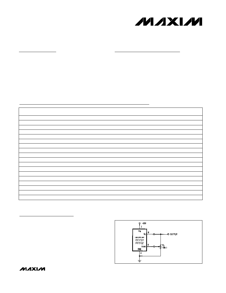
__________Typical Operating Circuit
19-0887; Rev 1; 8/99
For free samples & the latest literature: http://www.maxim-ic.com, or phone 1-800-998-8800.
For small orders, phone 1-800-835-8769.
PART
REF01EP
REF01EZ
REF01HP
0∞C to +70∞C
0∞C to +70∞C
0∞C to +70∞C
TEMP. RANGE
MAX TEMPCO
(ppm/∞C)
8.5
8.5
25
Ordering Information continued at end of data sheet.
±30
±30
±50
REF01HSA
REF01CP
REF01CSA
0∞C to +70∞C
0∞C to +70∞C
0∞C to +70∞C
25
65
65
±50
±100
±100
REF01CZ
0∞C to +70∞C
65
±100
REF01Z
REF02EP
REF02EZ
0∞C to +70∞C
0∞C to +70∞C
-55∞C to +125∞C
25
8.5
8.5
±50
±15
±15
REF02HP
0∞C to +70∞C
25
±25
REF02HSA
REF02CP
0∞C to +70∞C
0∞C to +70∞C
25
65
±25
±50
REF02CSA
REF02CZ
0∞C to +70∞C
0∞C to +70∞C
65
65
±50
±50
REF02Z
-55∞C to +125∞C
25
±25
INITIAL ERROR
(mV)
8 Plastic DIP
8 CERDIP
8 Plastic DIP
8 SO
8 Plastic DIP
8 SO
8 CERDIP
8 CERDIP
8 Plastic DIP
8 CERDIP
8 Plastic DIP
8 SO
8 Plastic DIP
8 SO
8 CERDIP
8 CERDIP
PIN-PACKAGE
Applications
A to D Converters
D to A Converters
Digital Voltmeters
Voltage Regulators
Threshold Detectors
Ordering Information
Reference with Trimmed Output
REF01CESA
-40∞C to +85∞C
65
±100
8 SO
REF02CESA
-40∞C to +85∞C
65
±50
8 SO
REF01/REF02
+5V, +10V Precision
Voltage References
2
_______________________________________________________________________________________
ABSOLUTE MAXIMUM RATINGS--REF01
Stresses beyond those listed under "Absolute Maximum Ratings" may cause permanent damage to the device. These are stress ratings only, and functional
operation of the device at these or any other conditions beyond those indicated in the operational sections of the specifications is not implied. Exposure to
absolute maximum rating conditions for extended periods may affect device reliability.
Input Voltage
REF01, A, E, H, All DICE ...................................................40V
REF01C .............................................................................30V
Power Dissipation
T099 (J) (derate at 7.1mW∞C above 80∞C) .................500mW
CERDIP (2) (derate at 6.7mW/∞C above 75∞C) ...........500mW
Plastic Dip (P) (derate at 5.6mW/∞C above 36∞C) ......500mW
Small Outline (S) (derate at 5.0mW/∞C above 55∞C) ..300mW
Output Short-Circuit Duration
(to ground or V
IN
) .....................................................Indefinite
Storage Temperature Range .............................-65∞C to +150∞C
Operating Temperature Range
REF01A, REF01 ............................................-55∞C to +125∞C
REF01E, REF01H, REF01C
(except REF01CESA) ..................................0∞C to +70∞C
REF01CESA ....................................................-40∞C to +85∞C
DICE Junction Temperature (T
j
) ........................-65∞C to +150∞C
Lead Temperature (soldering, 60s) .................................+300∞C
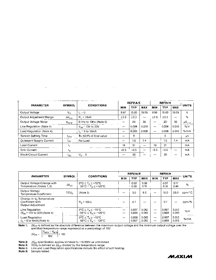
ELECTRICAL CHARACTERISTICS--REF01
(V
IN
= +15V, T
A
= +25∞C, unless otherwise noted.)
ELECTRICAL CHARACTERISTICS--REF01
(V
IN
= +15V, -55∞C
T
A
= +125∞C for REF01A and REF01, 0∞C
T
A
+70∞C for REF01E and REF01H, I
L
= 0mA, unless otherwise noted.)
Output Adjustment
The REF01 trim terminal can be used to adjust the volt-
age over a 10V±300mV range. This feature allows the
system designer to trim system errors by setting the ref-
erence to a voltage other than 10V, including 10.240V
for binary applications (see the Typical Operating
Circuit section).
Adjustment of the output does not significantly affect
the temperature performance of the device. The tem-
perature coefficient change is approximately
0.7ppm/∞C for 100mV of output adjustment.
REF01/REF02
+5V, +10V Precision
Voltage References
_______________________________________________________________________________________
3
ELECTRICAL CHARACTERISTICS--REF01
(V
IN
= +15V, T
A
= T
MIN
to T
MAX
, unless otherwise noted.)
ELECTRICAL CHARACTERISTICS--REF01 (continued)
(V
IN
= +15V, T
A
= +25∞C, unless otherwise noted.)
REF01/REF02
+5V, +10V Precision
Voltage References
4
_______________________________________________________________________________________
ABSOLUTE MAXIMUM RATINGS--REF02
Input Voltage
REF02, A, E, H, All DICE ...................................................40V
REF02C, D..........................................................................30V
Power Dissipation
T099 (J) (Derate at 7.1mW∞C above 80∞C).................500mW
CERDIP (2) (Derate at 6.7mW∞C above 75∞C) ...........500mW
Plastic Dip (P) (Derate at 5.6mW∞C above 36∞C) .......500mW
Small Outline (S) (Derate at 5.0mW∞C above 55∞C) ...300mW
Storage Temperature Range .............................-65∞C to +150∞C
Operating Temperature Range
REF02A, REF02 ............................................-55∞C to +125∞C
REF02E, REF02H (Except REF02CESA) ........0∞C to +70∞C
REF02C (except REF02CESA), REF02D ...........0∞C to +70∞C
REF02CESA ........................................................-40∞C to +85∞C
Lead Temperature (Soldering, 60s).................................+300∞C
DICE Junction Temperature (T
j
) ........................-65∞C to +150∞C
Output Short-Circuit Duration
(to Ground or V
IN
).....................................................Indefinite
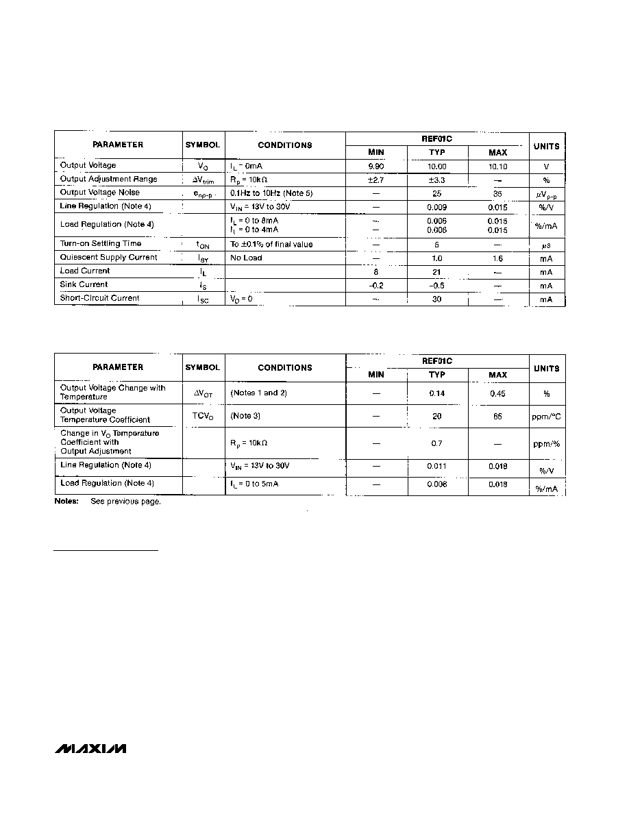
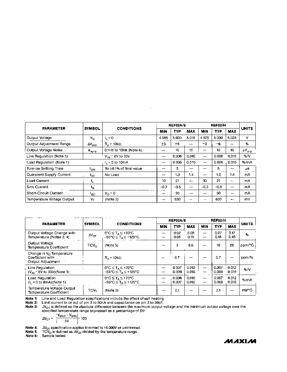
ELECTRICAL CHARACTERISTICS--REF01
(V
IN
= +15V, -55∞C
T
A =
+125∞C for REF02A and REF02, 0∞C
T
A
+70∞C for REF02E and REF02H, I
L
= 0mA, unless otherwise noted.)
Stresses beyond those listed under "Absolute Maximum Ratings" may cause permanent damage to the device. These are stress ratings only, and functional
operation of the device at these or any other conditions beyond those indicated in the operational sections of the specifications is not implied. Exposure to
absolute maximum rating conditions for extended periods may affect device reliability.
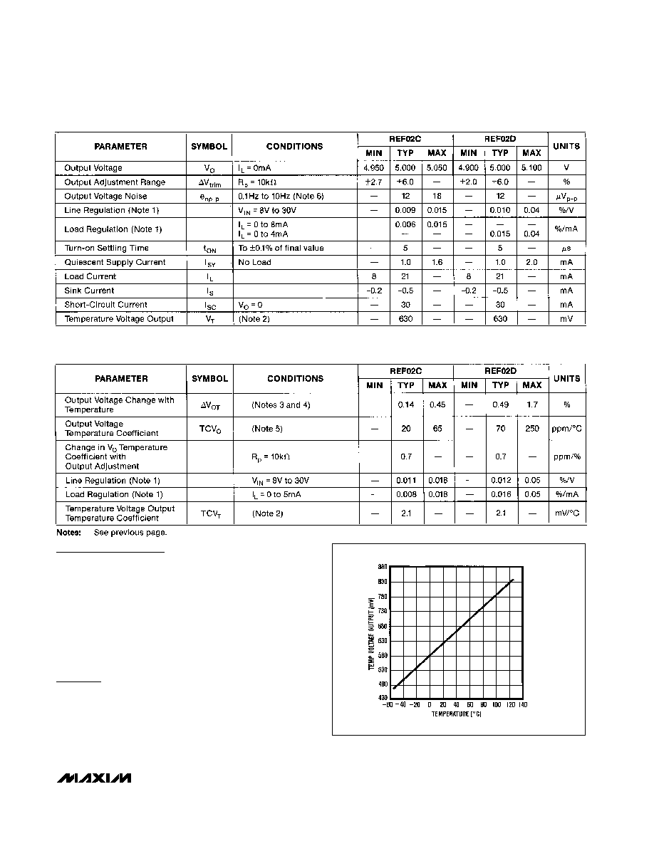
ELECTRICAL CHARACTERISTICS--REF02
(V
IN
= +15V, T
A
= +25∞C, unless otherwise noted.)
Output Adjustment
The REF02 trim terminal can be used to adjust the out-
put voltage over a 5V±300mV range. This feature
allows the system designer to trim system errors by set-
ting the reference to a voltage other than 5V (refer to
the Typical Operating Circuit section).
Adjustment of the output does not significantly affect
the temperature performance of the device. Typically,
the temperature coefficient change is 0.7ppm/∞C for
100mV of output adjustment.
Temperature Voltage Output
The REF02 provides a temperature-dependent output
voltage on the TEMP pin. This voltage is proportional
to the absolute temperature, and has a scale factor of
approximately 2.1mV/∞C (Figure 2).
Output Voltage = 2.1(T + 273)mV
where T = Temperature in ∞C
REF01/REF02
+5V, +10V Precision
Voltage References
_______________________________________________________________________________________
5
Figure 2. REF02 Temperature/Voltage Output vs. Temperature
ELECTRICAL CHARACTERISTICS--REF02
(V
IN
= +15V, T
A
= T
MIN
to T
MAX
and I
L
= 0mA, unless otherwise noted.)
ELECTRICAL CHARACTERISTICS--REF02
(V
IN
= +15V, T
A
= +25∞C, unless otherwise noted.)