 | –≠–ª–µ–∫—Ç—Ä–æ–Ω–Ω—ã–π –∫–æ–º–ø–æ–Ω–µ–Ω—Ç: REF01HF | –°–∫–∞—á–∞—Ç—å:  PDF PDF  ZIP ZIP |
PART
TEMP RANGE
MAX TEMPCO
(ppm/∞C)
INITIAL ERROR
(mV)
PIN-PACKAGE
REF01EP
0∞C to +70∞C
8.5
±30
8 Plastic DIP
REF01HP
0∞C to +70∞C
25
±50
8 Plastic DIP
REF01HSA
0∞C to +70∞C
25
±50
8 SO
REF01CP
0∞C to +70∞C
65
±100
8 Plastic DIP
REF01CSA
0∞C to +70∞C
65
±100
8 SO
REF01CESA
-40∞C to +85∞C
65
±100
8 SO
REF02EP
0∞C to +70∞C
8.5
±15
8 Plastic DIP
REF02HP
0∞C to +70∞C
25
±25
8 Plastic DIP
REF02HSA
0∞C to +70∞C
25
±25
8 SO
REF02CP
0∞C to +70∞C
65
±50
8 Plastic DIP
REF02CSA
0∞C to +70∞C
65
±50
8 SO
REF02CESA
-40∞C to +85∞C
65
±50
8 SO
General Description
The REF01/REF02 are industry-standard precision volt-
age references. The stable 10V output of the REF01
can be adjusted over a ±3% range with minimal effect
on temperature stability, while the 5V output REF02 can
be adjusted over a ±6% range. The 10V REF01 has a
single-supply operation over an input voltage range of
13V to 33V, while the 5V REF02 has a single-supply
operation over an input voltage range of 7V to 33V.
Both devices offer a low-current drain of 1mA. The
REF02 also provides a TEMP pin whose output voltage
varies linearly with temperature, making this device
suitable for a wide variety of temperature-sensing and
control applications. For new designs, please refer to
the MAX6035 or MAX6143 data sheets.
Features
o Pretrimmed to +5V, +10V ±0.3%
o Excellent Temperature Stability: 3ppm/∞C
o Low Noise: 10µV
P-P
(REF02)
o Low Supply Current: 1.4mA (max)
o Short-Circuit Proof
o Linear Temperature Transducer Output (REF02)
REF01/REF02
+5V, +10V Precision
Voltage References
________________________________________________________________ Maxim Integrated Products
1
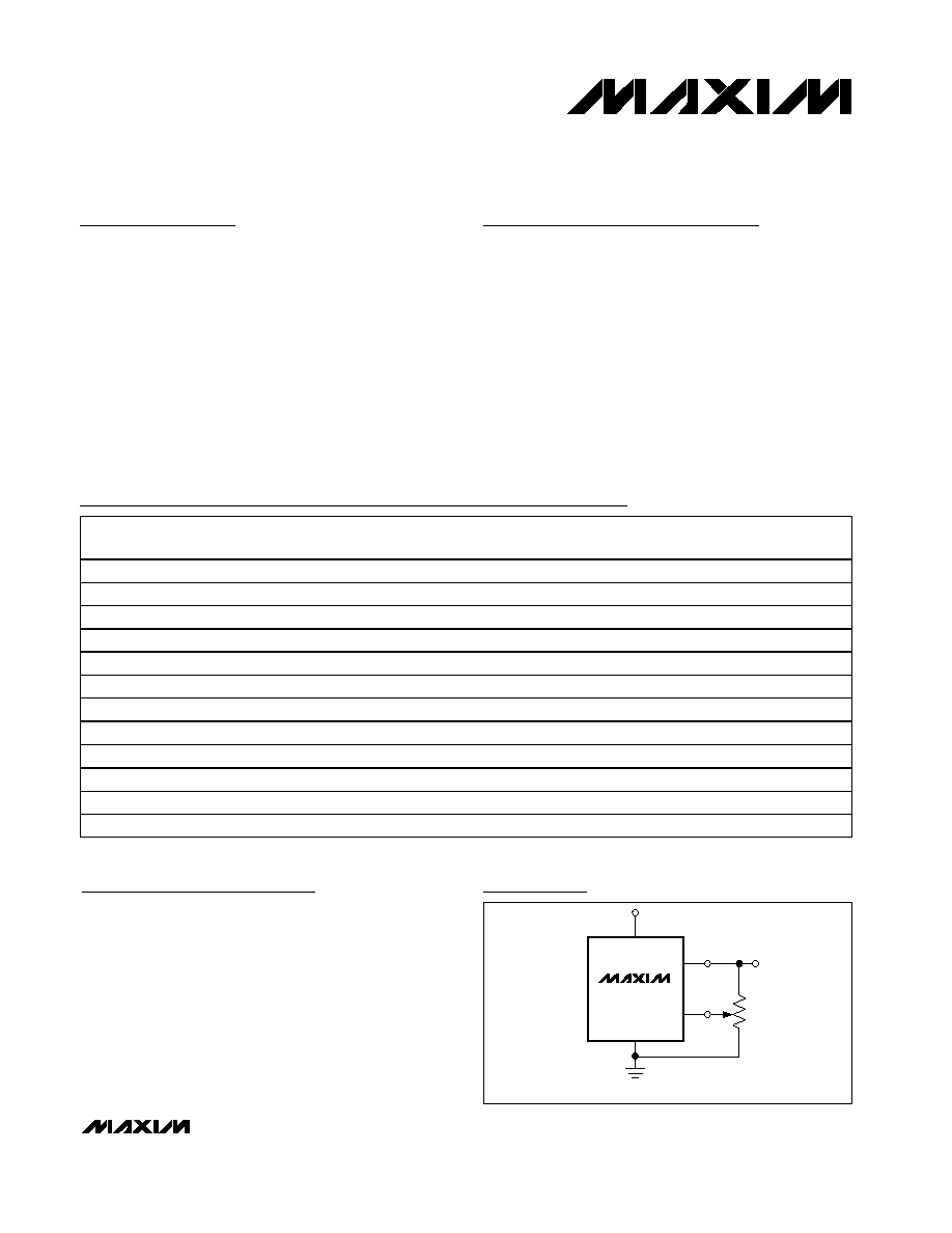
Ordering Information
REF01
REF02
OUTPUT
R
P
10k
6
5
TRIM
V
O
V
IN
-15V
4
GND
REFERENCE WITH TRIMMED OUTPUT.
2
Typical Operating Circuit
19-0887; Rev 3; 6/03
For pricing, delivery, and ordering information, please contact Maxim/Dallas Direct! at
1-888-629-4642, or visit Maxim's website at www.maxim-ic.com.
Ordering Information continued at end of data sheet.
Applications
Analog-to-Digitial Converters
Digitial-to-Analog Converters
Digital Voltmeters
Voltage Regulators
Threshold Detectors
REF01/REF02
+5V, +10V Precision
Voltage References
2
_______________________________________________________________________________________
ABSOLUTE MAXIMUM RATINGS≠REF01
ELECTRICAL CHARACTERISTICS≠REF01
(V
IN
= +15V, T
A
= +25∞C, unless otherwise noted.)
ELECTRICAL CHARACTERISTICS≠REF01
(V
IN
= +15V, -55∞C
T
A
+125∞C for REF01A and REF01, 0∞C T
A
+70∞C for REF01E and REF01H, I
L
= 0mA, unless otherwise
noted.)
Stresses beyond those listed under "Absolute Maximum Ratings" may cause permanent damage to the device. These are stress ratings only, and functional
operation of the device at these or any other conditions beyond those indicated in the operational sections of the specifications is not implied. Exposure to
absolute maximum rating conditions for extended periods may affect device reliability.
Input Voltage
REF01, A, E, H, All DICE .....................................................40V
REF01C ...............................................................................30V
Continuous Power Dissipation
T099 (J) (derate at 7.1mW∞C above +80∞C).................500mW
CERDIP (2) (derate at 6.7mW/∞C above +75∞C) .........500mW
Plastic Dip (P) (derate at 5.6mW/∞C above +36∞C) .....500mW
Small Outline (S) (derate at 5.0mW/∞C above +55∞C) ..300mW
Output Short-Circuit Duration
(to ground or V
IN
) .......................................................Indefinite
Storage Temperature Range .............................-65∞C to +150∞C
Operating Temperature Range
REF01A, REF01 ..............................................-55∞C to +125∞C
REF01E, REF01H, REF01C
(except REF01CESA)...........................................0∞C to +70∞C
REF01CESA ......................................................-40∞C to +85∞C
DICE Junction Temperature (Tj) ........................-65∞C to +150∞C
Lead Temperature (soldering, 60s) .................................+300∞C
REF01A/E
REF01/H
PARAMETER
SYMBOL
CONDITIONS
MIN
TYP
MAX
MIN
TYP
MAX
UNITS
Output Voltage
V
O
I
L
= 0
9.97
10.00
10.03
9.95
10.00
10.05
V
Output Adjustment Range
Vtrim
R
P
= 10k
±3.0
±3.3
±3.0
±3.3
%
Output Voltage Noise
en
P-P
0.1Hz to 10Hz (Note 1)
20
30
20
30
µV
P-P
Line Regulation
V
IN
= 13V to 33V (Note 2)
0.006
0.010
0.006
0.010
%/V
Load Regulation
I
L
= 0 to 10mA (Note 2)
0.005
0.008
0.006
0.010
%/mA
Turn-On Settling Time
t
ON
To ±0.1% of final value
5
5
µs
Quiescent Supply Current
I
SY
No load
1.0
1.4
1.0
1.4
mA
Load Current
I
L
10
21
10
21
mA
Sink Current
I
S
-0.3
-0.5
-0.3
-0.5
mA
Short-Circuit Current
I
SC
V
O
= 0V
30
30
mA
REF01A/E
REF01/H
PARAMETER
SYMBOL
CONDITIONS
MIN
TYP
MAX
MIN
TYP
MAX
UNITS
0∞C
T
A
+70∞C
0.02
0.06
0.07
0.17
Output Voltage Change with
Temperature (Notes 3, 4)
V
OT
-55∞C
T
A
+125∞C
0.06
0.15
0.18
0.45
%
Output Voltage Temperature
Coefficient
TCV
O
(Note 5)
3
8.5
10.0
25.0
ppm/∞C
Change in VO Temperature
Coefficient with Output
Adjustment
RP = 10k
0.7
0.7
ppm/%
0∞C
T
A
+70∞C
0.007
0.012
0.007
0.012
Line Regulation
(VIN = 13V to 33V) (Note 2)
-55∞C
T
A
+125∞C
0.009
0.015
0.009
0.015
%/V
0∞C
T
A
+70∞C
0.006
0.010
0.007
0.012
Load Regulation
(IL = 0 to 8mA) (Note 2)
-55∞C
T
A
+125∞C
0.007
0.012
0.009
0.015
%/mA

REF01/REF02
+5V, +10V Precision
Voltage References
_______________________________________________________________________________________
3
ELECTRICAL CHARACTERISTICS≠REF01 (continued)
(V
IN
= +15V, -55∞C
T
A
+125∞C for REF01A and REF01, 0∞C T
A
+70∞C for REF01E and REF01H, I
L
= 0mA, unless otherwise
noted.)
REF01C
PARAMETER
SYMBOL
CONDITIONS
MIN
TYP
MAX
UNITS
Output Voltage
V
O
I
L
= 0mA
9.90
10.00
10.10
V
Output Adjustment Range
V
trim
R
P
= 10k
±2.7
±3.3
%
Output Voltage Noise
e
nP-P
0.1Hz to 10Hz (Note 1)
25
35
µVP-P
Line Regulation
V
IN
= 13V to 30V (Note 2)
0.009
0.015
%/V
IL = 0 to 8mA
0.006
0.015
Load Regulation (Note 2)
IL = 0 to 4mA
0.006
0.015
%/mA
Turn-On Settling Time
tON
To ±0.1% of final value
5
µs
Quiescent Supply Current
ISY
No load
1.0
1.6
mA
Load Current
IL
8
21
mA
Sink Current
IS
-0.2
-0.5
mA
Short-Circuit Current
ISC
VO = 0V
30
mA
ELECTRICAL CHARACTERISTICS≠REF01
(V
IN
= +15V, T
A
= T
MIN
to T
MAX
, unless otherwise noted.)
REF01C
PARAMETER
SYMBOL
CONDITIONS
MIN
TYP
MAX
UNITS
Output Voltage Change with
Temperature
VOT
(Notes 3, 4)
0.14
0.45
%
Output Voltage Temperature
Coefficient
TCVO
(Note 5)
20
65
ppm/∞C
Change in VO Temperature
Coefficient with Output Adjustment
RP = 10k
0.7
ppm/%
Line Regulation
VIN = 13V to 30V (Note 2)
0.011
0.018
%/V
Load Regulation
IL = 0 to 5mA (Note 2)
0.008
0.018
%/mA
Output Adjustment
The REF01 trim terminal can be used to adjust the volt-
age over a 10V ±300mV range. This feature allows the
system designer to trim system errors by setting the ref-
erence to a voltage other than 10V, including 10.240V for
binary applications (see the Typical Operating Circuit).
Adjustment of the output does not significantly affect the
temperature performance of the device. The tempera-
ture coefficient change is approximately 0.7ppm/∞C for
100mV of output adjustment.
Note 1: Guaranteed by design for REF01HP, REF01HSA, REF01CP, REF01CSA, REF01CESA, REF02HP, REF02HSA, REF02CP,
REF02CSA, REF02CESA. Sample tested for all other grades and packages.
Note 2: Line and load regulation specifications include the effect of self heating.
Note 3:
V
OT
is defined as the absolute difference between the maximum output voltage and the minimum output voltage over the
specified temperature range expressed as a percentage of 10V.
Note 4:
V
OT
specification applies trimmed to +10.000V or untrimmed.
Note 5: TCV
O
is defined as
V
OT
divided by the temperature range.
V
OT
=
◊
V
- V
10V
100
MAX
MIN
REF01/REF02
+5V, +10V Precision
Voltage References
4
_______________________________________________________________________________________
ABSOLUTE MAXIMUM RATINGS≠REF02
Input Voltage
REF02, A, E, H, All DICE .....................................................40V
REF02C, D...........................................................................30V
Continuous Power Dissipation
T099 (J) (derate at 7.1mW∞C above +80∞C).................500mW
CERDIP (2) (derate at 6.7mW/∞C above +75∞C) .........500mW
Plastic Dip (P) (derate at 5.6mW/∞C above +36∞C) .....500mW
Small Outline (S) (derate at 5.0mW/∞C above +55∞C) ..300mW
Storage Temperature Range .............................-65∞C to +150∞C
Operating Temperature Range
REF02A, REF02 ..............................................-55∞C to +125∞C
REF02E, REF02H (except REF02CESA)..............0∞C to +70∞C
REF02C (except REF02CESA), REF02D .............0∞C to +70∞C
REF02CESA ......................................................-40∞C to +85∞C
Lead Temperature (soldering, 60s) .................................+300∞C
DICE Junction Temperature (Tj) ........................-65∞C to +150∞C
Output Short-Circuit Duration
(to ground or V
IN
) .......................................................Indefinite
ELECTRICAL CHARACTERISTICS≠REF02
(V
IN
= +15V, -55∞C
T
A
+125∞C for REF02A and REF02, 0∞C T
A
+70∞C for REF02E and REF02H, I
L
= 0mA, unless otherwise
noted.)
ELECTRICAL CHARACTERISTICS≠REF02
(V
IN
= +15V, T
A
= +25∞C, unless otherwise noted.)
REF02A/E
REF02/H
PARAMETER
SYMBOL
CONDITIONS
MIN
TYP
MAX
MIN
TYP
MAX
UNITS
Output Voltage
VO
IL = 0
4.985
5.000
5.015
4.975
5.000
5.025
V
Output Adjustment Range
Vtrim
RP = 10k
±3
±6
±3
±6
%
Output Voltage Noise
enP-P
0.1Hz to 10Hz (Note 6)
10
15
10
15
µVP-P
Line Regulation
VIN = 8V to 33V (Note 7)
0.006
0.010
0.006
0.010
%/V
Load Regulation
IL = 0 to 10mA (Note 7)
0.005
0.010
0.006
0.010
%/mA
Turn-On Settling Time
tON
To ±0.1% of final value
5
5
µs
Quiescent Supply Current
ISY
No load
1.0
1.4
1.0
1.4
mA
Load Current
IL
10
21
10
21
mA
Sink Current
IS
-0.3
-0.5
-0.3
-0.5
mA
Short-Circuit Current
ISC
VO = 0V
30
30
mA
Temperature Voltage
Output
VT
(Note 8)
630
630
mV
REF02A/E
REF02/H
PARAMETER
SYMBOL
CONDITIONS
MIN
TYP
MAX
MIN
TYP
MAX
UNITS
0∞C
TA +70∞C
0.02
0.06
0.07
0.17
Output Voltage Change with
Temperature (Notes 9, 10)
VOT
-55∞C
TA +125∞C
0.06
0.15
0.18
0.45
%
Output Voltage Temperature
Coefficient
TCVO
(Note 11)
3
8.5
10
25
ppm/∞C
Change in VO Temperature
Coefficient with Output
Adjustment
RP = 10k
0.7
0.7
ppm/%
0∞C
TA +70∞C
0.007
0.012
0.007
0.012
Line Regulation
(V I N = 8V to 33V) (Note 7)
-55∞C
TA +125∞C
0.009
0.015
0.009
0.015
%/V
0∞C
TA +70∞C
0.006
0.010
0.007
0.012
Load Regulation
(IL = 0 to 8mA) (Note 7)
-55∞C
TA +125∞C
0.007
0.012
0.009
0.015
%/mA
Stresses beyond those listed under "Absolute Maximum Ratings" may cause permanent damage to the device. These are stress ratings only, and functional
operation of the device at these or any other conditions beyond those indicated in the operational sections of the specifications is not implied. Exposure to
absolute maximum rating conditions for extended periods may affect device reliability.

REF01/REF02
+5V, +10V Precision
Voltage References
_______________________________________________________________________________________
5
ELECTRICAL CHARACTERISTICS≠REF02 (continued)
(V
IN
= +15V, -55∞C
T
A
+125∞C for REF02A and REF02, 0∞C T
A
+70∞C for REF02E and REF02H, I
L
= 0mA, unless otherwise
noted.)
REF02A/E
REF02/H
UNITS
PARAMETER
SYMBOL
CONDITIONS
MIN
TYP
MAX
MIN
TYP
MAX
Temperature Voltage Output
Temperature Coefficient
TCVT
(Note 8)
2.1
2.1
mV/∞C
ELECTRICAL CHARACTERISTICS≠REF02
(V
IN
= +15V, T
A
= +25∞C, unless otherwise noted.)
REF02C
REF02D
PARAMETER
SYMBOL
CONDITIONS
MIN
TYP
MAX
MIN
TYP
MAX
UNITS
Output Voltage
VO
IL = 0mA
4.950
5.000
5.050
4.900
5.000
5.100
V
Output Adjustment Range
Vtrim
RP = 10k
±2.7
±6.0
±2.0
±6.0
%
Output Voltage Noise
enP-P
0.1Hz to 10Hz
(Note 6)
12
18
12
µVP-P
Line Regulation
VIN = 8V to 30V (Note 7)
0.009
0.015
0.010
0.04
%/V
IL = 0 to 8mA
0.006
0.015
Load Regulation (Note 7)
IL = 0 to 4mA
0.015
0.04
%/mA
Turn-On Settling Time
tON
To ±0.1% of final value
5
5
µs
Quiescent Supply Current
ISY
No load
1.0
1.6
1.0
2.0
mA
Load Current
IL
8
21
8
21
mA
Sink Current
IS
-0.2
-0.5
-0.2
-0.5
mA
Short-Circuit Current
ISC
VO = 0V
30
30
mA
Temperature Voltage Output
VT
(Note 8)
630
630
mV
ELECTRICAL CHARACTERISTICS≠REF02
(V
IN
= +15V, T
A
= T
MIN
to T
MAX
, I
L
= 0mA, unless otherwise noted.)
REF02C
REF02D
UNITS
PARAMETER
SYMBOL
CONDITIONS
MIN
TYP
MAX
MIN
TYP
MAX
Output Voltage Change with
Temperature
VOT
(Notes 9, 10)
0.14
0.45
0.49
1.7
%
Output Voltage Temperature
Coefficient
TCVO
(Note 11)
20
65
70
250
ppm/∞C
Change in VO Temperature
Coefficient with Output
Adjustment
RP = 10k
0.7
0.7
ppm/%
Line Regulation
VIN = 8V to 30V (Note 7)
0.011
0.018
0.012
0.05
%/V
Load Regulation
IL = 0 to 5mA (Note 7)
0.008
0.018
0.016
0.05
%/mA
Temperature Voltage Output
Temperature Coefficient
TCVT
(Note 8)
2.1
2.1
mV/∞C