 | –≠–ª–µ–∫—Ç—Ä–æ–Ω–Ω—ã–π –∫–æ–º–ø–æ–Ω–µ–Ω—Ç: 124RPFI | –°–∫–∞—á–∞—Ç—å:  PDF PDF  ZIP ZIP |

1
Memory
All data sheets are subject to change without notice
(858) 503-3300 - Fax: (858) 503-3301 - www.maxwell.com
Low-Power Quad
Operational Amplifier
©2002 Maxwell Technologies
All rights reserved.
124
04.02.02 Rev 5
F
EATURES
:
∑ R
AD
-P
AK
Æ technology-hardened against natural space radi-
ation
∑ Total dose hardness:
- > 100 krad (Si), depending upon space mission
∑ Excellent Single Event Effects:
∑ - SELTH LET = > 90 MeV/mg/cm2
∑ Package: -14 pin Rad-PakÆ flat pack
∑ Internally frequency compensated for unity gain
∑ Large DC voltage gain
∑ Wide bandwidth (unity gain): 1 MHz
∑ Large output voltage swing 0V to V+ -1.5V
∑ Input common - mode voltage range includes ground
∑ Wide power supply range:
- Single supply 3V to 32V
- Dual supply ±1.5V to ±16V
∑ Very low current drain (essentially independent of supply
voltage): 700 uA
∑ Low input biasing current: 45 nA
∑ Low input offset voltage and current: 2mV, 5nA
∑ Differential input voltage range equal to the power supply
voltage
D
ESCRIPTION
:
Maxwell Technologies's 124 independent, high gain, internally
frequency compensated operational amplifiers feature a
greater than 100 krad (Si) total dose tolerance, depending
upon space mission. Using Maxwell's radiation-hardened
Rad-PakÆ packaging technology, the 124 is designed specifi-
cally to operate from a single power supply over a wide range
of voltages. The 124 also features operation from split power
supplies, and the low power supply current drain is indepen-
dent of the magnitude of the power supply voltage.
Maxwell Technologies' patented R
AD
-P
AK
Æ packaging technol-
ogy incorporates radiation shielding in the microcircuit pack-
age. It eliminates the need for box shielding while providing
the required radiation shielding for a lifetime in orbit or space
mission. In a GEO orbit, R
AD
-P
AK
provides greater than 100
krad (Si) radiation dose tolerance. This product is available
with screening up to Class S.
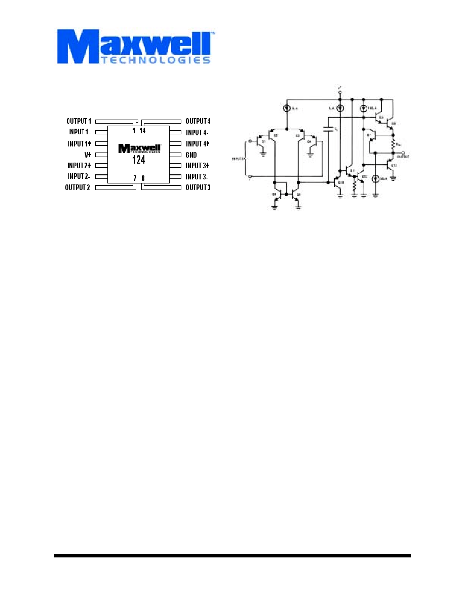
Logic Diagram

124
Memory
2
All data sheets are subject to change without notice
©2002 Maxwell Technologies
All rights reserved.
Low-Power Quad Operational Amplifier
04.02.02 Rev 5
T
ABLE
1. P
INOUT
D
ESCRIPTION
P
IN
S
YMBOL
D
ESCRIPTION
1, 7, 8, 14
OUTPUT 1 - 4
Ouput
2, 6, 9, 13
INPUT 1- ≠ 4-
Input (-)
3, 5, 10, 12
INPUT 1+ ≠ 4+
Input (+)
4
V+
Power Supply
11
GND
Ground
T
ABLE
2. 124 A
BSOLUTE
M
AXIMUM
R
ATINGS
P
ARAMETER
S
YMBOL
M
IN
M
AX
U
NIT
Supply Voltage
V+
32
V
Differential Input Voltage
32
V
Input Voltage
-0.3
+32
V
Input Current (V
IN
< -0.3V)
1
1. This input current will only exist when the voltage at any of the input leads is driven negative. It is due to the collector-base
junction of the input PNP transistors becoming forward biased and thereby acting as input diode clamps. In addition to this
diode action, there is also lateral NPN parasitic transistor action on the IC chip. This transistor action can cause the output
voltages of the op amps to go to the V+ voltage level (or to ground for a large overdrive) for the time duration that an input is
driven negative. This is not destructive and normal output states will re-establish when the input voltage, which was negative,
again returns to a value greater than -0.3V (at 25∞C).
50
mA
Output Short-Circuit to GND (One Amplifier)
V+ < 15V, TA = 25∞C
2
2. Short circuits from the output to V+ can cause excessive heating and eventual destruction. When considering short circuits to
ground, the maximum output current is approximately 40 mA independent of the magnitude of V+. At values of supply voltage
in excess of +15V, continuous short-circuits can exceed the power dissipation ratings and cause eventual destruction.
Destructive dissipation can result from simultaneous shorts on all amplifiers.
Continuous
Storage Temperature Range
T
S
-65
150
∞C
Operating Temperature Range
T
A
-55
125
∞C
ESD Tolerance
3
3. Human body model, 1.5 k
in series with 100 pF.
250
V
T
ABLE
3. D
ELTA
L
IMITS
P
ARAMETER
V
ARIATION
I
CC
±10% of specified value in Table 4

124
Memory
3
All data sheets are subject to change without notice
©2002 Maxwell Technologies
All rights reserved.
Low-Power Quad Operational Amplifier
04.02.02 Rev 5
T
ABLE
4. 124 E
LECTRICAL
C
HARACTERISTICS
(V+ = 5.0V, T
A
= -55
TO
+125∞C,
UNLESS
OTHERWISE
SPECIFIED
)
P
ARAMETER
S
YMBOL
T
EST
C
ONDITIONS
S
UB
G
ROUPS
M
IN
T
YP
M
AX
U
NITS
Supply Current
I
CC
Over Full Temperature Range
RL =
On All Op Amps
V+ = 30V
V+ = 5V
1, 2, 3
1.5
0.7
3
1.2
mA
Common-Mode Rejection Ratio
CMRR
DC, V
CM
= 0V to V+ -1.5V,
T
A
= 25∞C
1
70
85
dB
Power Supply Rejection Ratio
PSRR
V+ = 5V to 30V
T
A
= 25∞C
1
65
100
dB
Amplifier-to-Amplifier Coupling
1
1. Due to proximity of external components, insure that coupling is not originating via stray capacitance between these external parts. This typically can
be detected as this type of capacitance increases at higher frequencies.
f = 1 kHz to 20 kHz, T
A
= 25∞C
(Input Referred)
1
-120
dB
Short Circuit to Ground
2
2. Short circuits from the output to V+ can cause excessive heating and eventual destruction. When considering short circuits to ground, the maximum
output current is approximately 40 mA independent of the magnitude of V+. At values of supply voltage in excess of +15V, continuous short-circuits
can exceed the power dissipation ratings and cause eventual destruction. Destructive dissipation can result from simultaneous shorts on all amplifi-
ers.
I
OS
V+ = 15V, TA = 25∞C
1
40
mA
Input Offset Voltage
3
3. VO@1.4V, RS=0
with V+ from 5V to 30V; and over the full input common-mode range (0V to V+ -1.5V).
V
IO
1, 2, 3
7
mV
Input Offset Voltage Drift
R
S
= 0
1, 2, 3
7
µV/∞C
Input Offset Current
I
OS
I
IN
(+)-I
IN
(-), V
CM
= 0V
1, 2, 3
---
--
100
nA
Input Offset Current Drift
R
S
= 0
1, 2, 3
---
10
--
pA/∞C
Input Bias Current
lib
I
IN
(+) or I
IN
(-)
1, 2, 3
---
40
300
nA
Input Common-Mode Voltage
Range
4
4. The input common-mode voltage of either input signal voltage should not be allowed to go negative by more than 0.3V (at 25∞C). The upper end of
the common-mode voltage range is V+ -1.5V (at 25∞C), but either or both inputs can go to +32V without damage independent of the magnitude of
V+.
V+ = +30V
1, 2, 3
0
V+ -2
V
Large Signal Voltage Gain
A
VS
V+ = +15V
(V
O
Swing = 1V to 11V)
RL> 2 K
1, 2, 3
25
V/mV
Output Voltage Swing
V
OH
V+ = 30V, R
L
= 2 k
R
L
= 10 k
1, 2, 3
26
27
28
V
V
OL
V+ = 5V, R
L
= 10 k
1, 2, 3
5
20
mV
Output Current
Source
VO = 2V, V
IN
+
= +1V
V
IN
-
= 0V
V
+
= 15V
V
IN
+
= +1V
V
IN
-
= 0V
V
+
= 15V
1, 2, 3
20
mA
Sink
1, 2, 3
15

124
Memory
4
All data sheets are subject to change without notice
©2002 Maxwell Technologies
All rights reserved.
Low-Power Quad Operational Amplifier
04.02.02 Rev 5
F
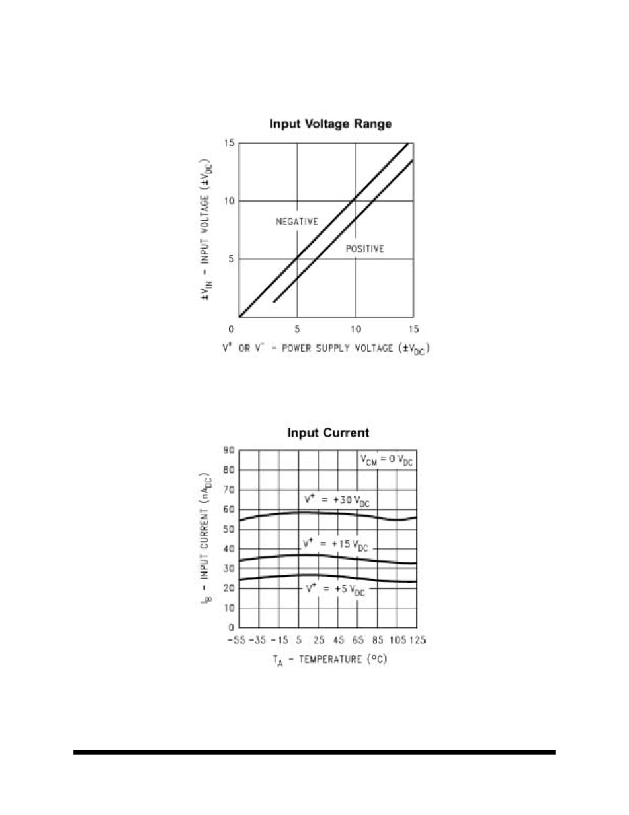
IGURE
1. I
NPUT
V
OLTAGE
R
ANGE
F
IGURE
2. I
NPUT
C
URRENT

124
Memory
5
All data sheets are subject to change without notice
©2002 Maxwell Technologies
All rights reserved.
Low-Power Quad Operational Amplifier
04.02.02 Rev 5
F
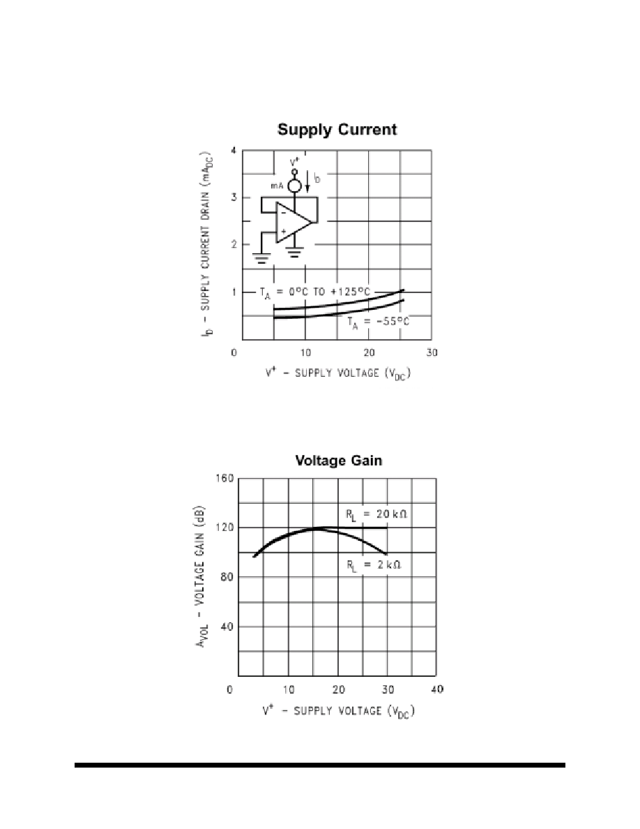
IGURE
3. S
UPPLY
C
URRENT
F
IGURE
4. V
OLTAGE
G
AIN
