 | –≠–ª–µ–∫—Ç—Ä–æ–Ω–Ω—ã–π –∫–æ–º–ø–æ–Ω–µ–Ω—Ç: 139RPFI | –°–∫–∞—á–∞—Ç—å:  PDF PDF  ZIP ZIP |

1
Memory
All data sheets are subject to change without notice
(858) 503-3300 - Fax: (858) 503-3301 - www.maxwell.com
Quad Comparators,
139
©2001 Maxwell Technologies
All rights reserved.
Low Offset Voltage
12.13.01 Rev1
1000522
F
EATURES
:
∑ Rad-PakÆ technology-hardened against natural space
radiation
∑ Total dose hardness:
- >100 krad (Si), depending upon orbit and space mission
∑ Single Event Effects:
- SEL > 59.8 MeV/mg/cm
2
∑ Package:
∑ - 14 pin Rad-PakÆ flat package
∑ Wide supply voltage range
- 2 VDC to 36 VDC or ±1 VDC to ±18 VDC
∑ Very low supply current drain:
- (0.8 mA) - independent of supply voltage
∑ Low input biasing current: 25 nA
∑ Differential input voltage range equal to the power supply
voltage
∑ Low output saturation voltage: 250 mV at 4 mA
∑ Power drain suitable for battery operation
∑ Allows sensing near GND
∑ Eliminates need for dual supplies
∑ Output voltage compatible with TTL, DTL, ECL, MOS and
CMOS logic systems
∑ Low input offset current and offset voltage:
- +5 nA, +3 mV
D
ESCRIPTION
:
Maxwell Technologies 139 consisting of four independent pre-
cision voltage comparators, features a greater than 100 krad
(Si) total dose tolerance, depending upon space mission.
Using Maxwell Technologies radiation- hardened Rad-PakÆ
packaging technology, the 139 has an offset voltage specifica-
tion as low as 2 mV max for all four comparators. The 139
was also designed specifically to operate from a single power
supply over a wide range of voltages. Operation from split
power supplies is possible and the low power supply current
drain is independent of the magnitude of the power supply
voltage. These comparators also have a unique characteristic
in that the input common-mode voltage range includes
ground, even though operated from a single power supply
voltage.
Maxwell Technologies' patented R
AD
-P
AK
packaging technol-
ogy incorporates radiation shielding in the microcircuit pack-
age. It eliminates the need for box shielding while providing
the required radiation shielding for a lifetime in orbit or space
mission. In a GEO orbit, R
AD
-P
AK
provides greater than 100
krad (Si) radiation dose tolerance. This product is available
with screening up to Class S.
Logic Diagram

Memory
2
All data sheets are subject to change without notice
©2001 Maxwell Technologies
All rights reserved.
Quad Comparators, Low Offset Voltage
139
12.13.01 Rev1
1000522
T
ABLE
1. P
INOUT
D
ESCRIPTION
P
IN
S
YMBOL
D
ESCRIPTION
2, 1, 14, 13
OUTPUT1 - 4
Output Signal
4, 6, 8, 10
INPUT1- ≠ 4
Negative Input Signal
5, 7, 9, 11
INPUT+ ≠ 4
Positive Input Signal
3
V+
Positive Voltage
12
GND
Ground
T
ABLE
2. 139 A
BSOLUTE
M
AXIMUM
R
ATINGS
P
ARAMETER
S
YMBOL
M
IN
M
AX
U
NIT
Supply Voltage (V+ - V-)
V+ - V-
36 V
DC
or ±18 V
DC
V
Differential Input Voltage
1
1. Positive excursions of input voltage may exceed the power supply level. As long as the other voltage remains within the com-
mon-mode range, the comparator will provide a proper output state. The low output voltage state must not be less than -0.3
V
DC
(or 0.3 V
DC
below the magnitude of the negative power supply, if used) (at 25∞C).
--
36
V
Input Voltage
-0.3
+36
V
Open Short-Circuit to Ground
2
2. Short Circuits from the output to V+ can cause excessive heating and eventual destruction. When considering short circuits to
ground, the maximum output current is ~20mA independent of the magnitude of V+.
Continuous
Input Current (V
IN
< -0.3V
DC
)
--
50
mA
Power Dissipation
P
D
--
1
W
Storage Temperature Range
T
S
-65
150
∞
C
Operating Temperature Range
T
A
-55
125
∞
C
ESD Tolerance
3
3. 1.5 k
in series with 100 pF.
--
600
V
T
ABLE
3. D
ELTA
L
IMITS
P
ARAMETER
V
ARIATION
I
CC
±10% of specified value in Table 5
T
ABLE
4. 139 R
ECOMMENDED
O
PERATING
C
ONDITIONS
P
ARAMETER
S
YMBOL
M
IN
M
AX
U
NIT
Supply Voltage
V+ - V-
36 V
DC
or ±18 V
DC
V

Memory
3
All data sheets are subject to change without notice
©2001 Maxwell Technologies
All rights reserved.
Quad Comparators, Low Offset Voltage
139
12.13.01 Rev1
1000522
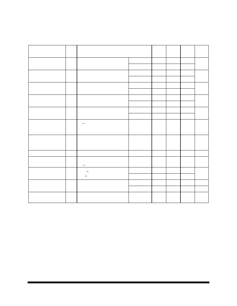
T
ABLE
5. 139 E
LECTRICAL
C
HARACTERISTICS
(V+ = 5V, T
A
= -55
TO
125∞C,
UNLESS
OTHERWISE
SPECIFIED
)
P
ARAMETER
S
YMBO
L
T
EST
C
ONDITIONS
M
IN
T
YP
M
AX
U
NIT
Input Offset Voltage
V
IO
1
1. At output switch point, V
O
=1.4V, RS=0
with V+ from 5V
DC
to 30 V
DC
; and over the full input common-mode range (0V
DC
to
V+-1.5V
DC
).
+25∞C
--
2
5
mV
DC
-55 to 125∞C
--
--
9
Input Bias Current
I
IB
I
IN
(+) or I
IN
(-) with Output in Linear
Range,
2
, V
CM
= 0V
2. The direction of the input current is out of the IC due to the PNP input stage. This current essentially constant, independent of
the state of the output so no loading change exists on the reference or input lines.
+25∞C
--
25
100
nA
DC
-55 to 125∞C
--
--
300
Input Offset Current
I
IO
I
IN
(+) - I
IN
(-), V
CM
= 0V
+25∞C
--
3
25
nA
DC
-55 to 125∞C
--
--
100
Input Common Mode
Voltage Range
V
CM
V+ = 30 V
DC
3
3. The input common-mode voltage or either input voltage signal should not be allowed to go negative by more than 0.3V. The
upper end of the common-mode voltage range is V+-1.5V at 25∞C, but either or both inputs can go to +30V without damage,
independent of the magnitude of V+.
+25∞C
0
V+ -1.5
V
DC
-55 to 125∞C
0
--
V+ -2.0
Supply Current
I
CC
R
L
=
on all comparators, V+ = 30V +25∞C
--
0.8
2.0
mA
DC
-55 to 125∞C
--
--
3.0
Voltage Gain
A
V
R
L
> 15k
, V+=15V
DC
;
V
O
= 1V
DC
to 11 V
DC
( To support large V
O
swing)
+25∞C
50
200
--
V/mV
Large Signal Response
Time
t
r
V
IN
= TTL Logic Swing,
V
REF
= 1.4V, V
RL
= 5
V
DC
,
R
I
= 5.1k
2
+25∞C
--
300
--
ns
Response Time
t
Rtil
V
RL
= 5
V
DC
, R
L
= 5.1k
4
4. The response time specified is for a 100mV input step with 5 mV overdrive. For larger overdrive signals 300 ns can be
obtained.
+25∞C
--
1.3
--
µs
Output Sink Current
I
SINK
V
IN
(-) = 1V
DC
, V
IN
(+) = 0,
V
O
< 1.5V
DC
+25∞C
6.0
16
--
mA
DC
Saturation Voltage
V
SAT
V
IN
(-) > 1V, V
IN
(+) = 0,
I
SINK
< 4 mA
+25∞C
--
250
400
mV
DC
-55 to 125∞C
--
--
700
Output Leakage Current
I
CEX
V
IN
(+) = 1V
DC
, V
IN
(-) = 0,
V
O
= 5V
DC
V
IN
(-) = 0
+25∞C
--
0.1
--
nA
DC
-55 to 125∞C
--
--
1.0
µA
DC
Differential Input Voltage
V
diff
Keep all V
IN's
> 0 V
DC
(or V- if used)
5
5. Positive excursions of input voltage may exceed the power level as long as the other voltage remains within the common
mode range, the comparator will provide a proper output state. The low input voltage state must not be less than -0.3 V
DC
(or
0.3V
DC
below the magnitude of the negative power supply, if used) (at 25∞C).
-55 to 125∞C
--
--
36
V
DC

Memory
4
All data sheets are subject to change without notice
©2001 Maxwell Technologies
All rights reserved.
Quad Comparators, Low Offset Voltage
139
12.13.01 Rev1
1000522
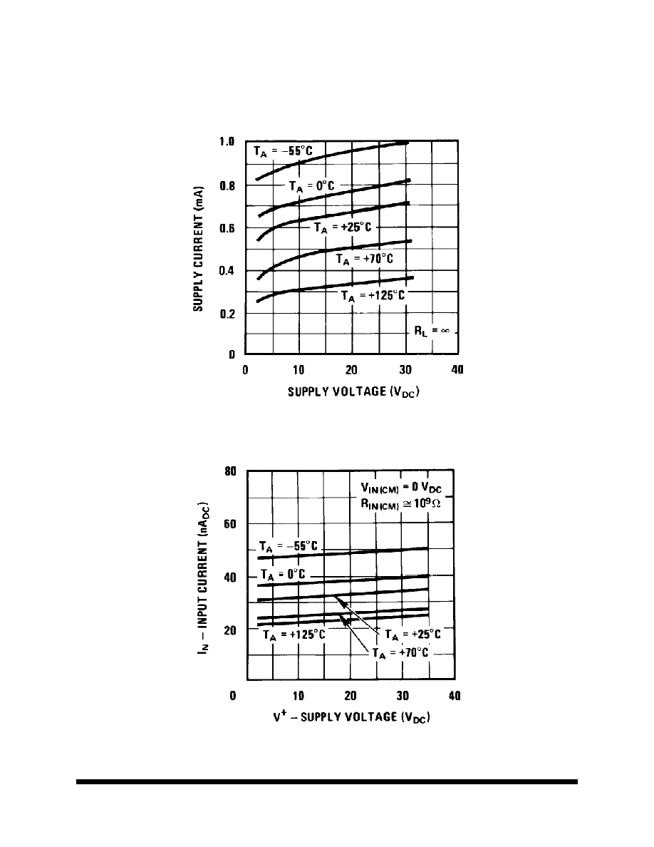
F
IGURE
1. S
UPPLY
C
URRENT
F
IGURE
2. I
NPUT
C
URRENT

Memory
5
All data sheets are subject to change without notice
©2001 Maxwell Technologies
All rights reserved.
Quad Comparators, Low Offset Voltage
139
12.13.01 Rev1
1000522
F
IGURE
3. O
UTPUT
S
ATURATION
V
OLTAGE
F
IGURE
4. R
ESPONSE
T
IME
FOR
V
ARIOUS
I
NPUT
O
VERDRIVES
≠ N
EGATIVE
T
RANSITION


