1
Memory
All data sheets are subject to change without notice
(858) 503-3300 - Fax: (858) 503-3301 - www.maxwell.com
1 Megabit (128K x 8-Bit) -
OTP EPROM
27C010T
�2001 Maxwell Technologies
All rights reserved.
12.12.01 Rev 2
F
EATURES
:
� 128k x 8 Bit OTP EPROM organization
� R
AD
-P
AK
� radiation-hardened against natural space radia-
tion
� Total dose hardness:
- >100 krad (Si), depending upon space mission
� Excellent Single Event Effects:
- SEL
TH
LET: > 80 MeV/mg/cm
2
- SEU
TH
LET (read mode): >80 Mev/mg/cm
2
� Package:
- 32 pin R
AD
-P
AK
� flat pack
- Weight - 6.0 grams
� Fast access time:
- 120, 150, 200 ns (max) times available
� Low power consumption:
- Active mode: 50 mW/MHz (typ)
- Standby mode: 5�W (typ)
� High speed page and word programming:
- Page programming time: 14 sec (typ)
� Programming power supply:
- V
PP
= 12.5 V � 0.3 V
� One-time Programmable
� Pin Arrangement
- JEDEC standard byte-wide EPROM
- Flash memory and mask ROM compatible
D
ESCRIPTION
:
Maxwell Technologies
' 27C010T high density 1 Megabit
One-time Programmable Electrically Programmable Read
Only Memory microcircuit features a greater than 100 krad (Si)
total dose tolerance, depending upon space mission. The
27C010T features fast address times and low power dissipa-
tion. The 27C010T offers high speed programming using page
programming mode. The 27C010T is offered in JEDEC-Stan-
dard Byte-Wide EPROM pinouts, which allows socket replace-
ment with Flash Memory and Mask ROMs.
Maxwell Technologies' patented R
AD
-P
AK
� packaging technol-
ogy incorporates radiation shielding in the microcircuit pack-
age. It eliminates the need for box shielding while providing
the required radiation shielding for a lifetime in orbit or space
mission. In a GEO orbit, R
AD
-P
AK
provides greater than 100
krad (Si) radiation dose tolerance. This product is available
with screening up to Class S.
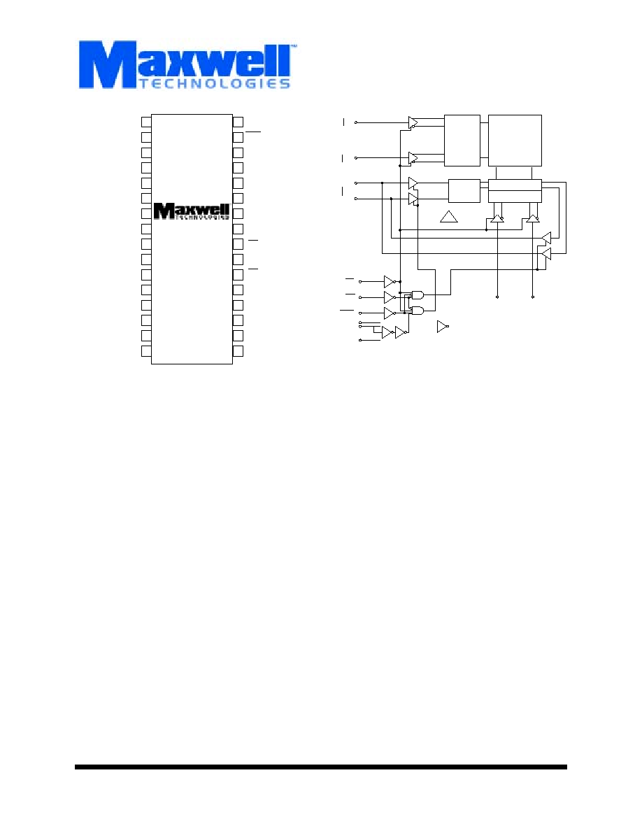
1024 x 1024
Memory Matrix
X-Decoder
Input
Data
Control
Y-Gating
Y-Decoder
H
H
: High Threshold Inverter
V
SS
V
PP
V
CC
PGM
OE
CE
I/O7
I/O0
A16
A12
A9
A5
A0-A4
A10-A11
1
16
17
32
V
CC
PGM
NC
A14
A13
A8
A9
A11
OE
A10
CE
I/O7
I/O6
I/O5
I/O4
I/O3
V
SS
I/O2
I/O1
I/O0
A1
A0
A2
A3
A4
A5
A6
A7
A12
A15
A16
V
PP
27C010T
Logic Diagram

Memory
2
All data sheets are subject to change without notice
�2001 Maxwell Technologies
All rights reserved.
1 Megabit (128K x 8-Bit) - OTP EPROM
27C010T
12.12.01 Rev 2
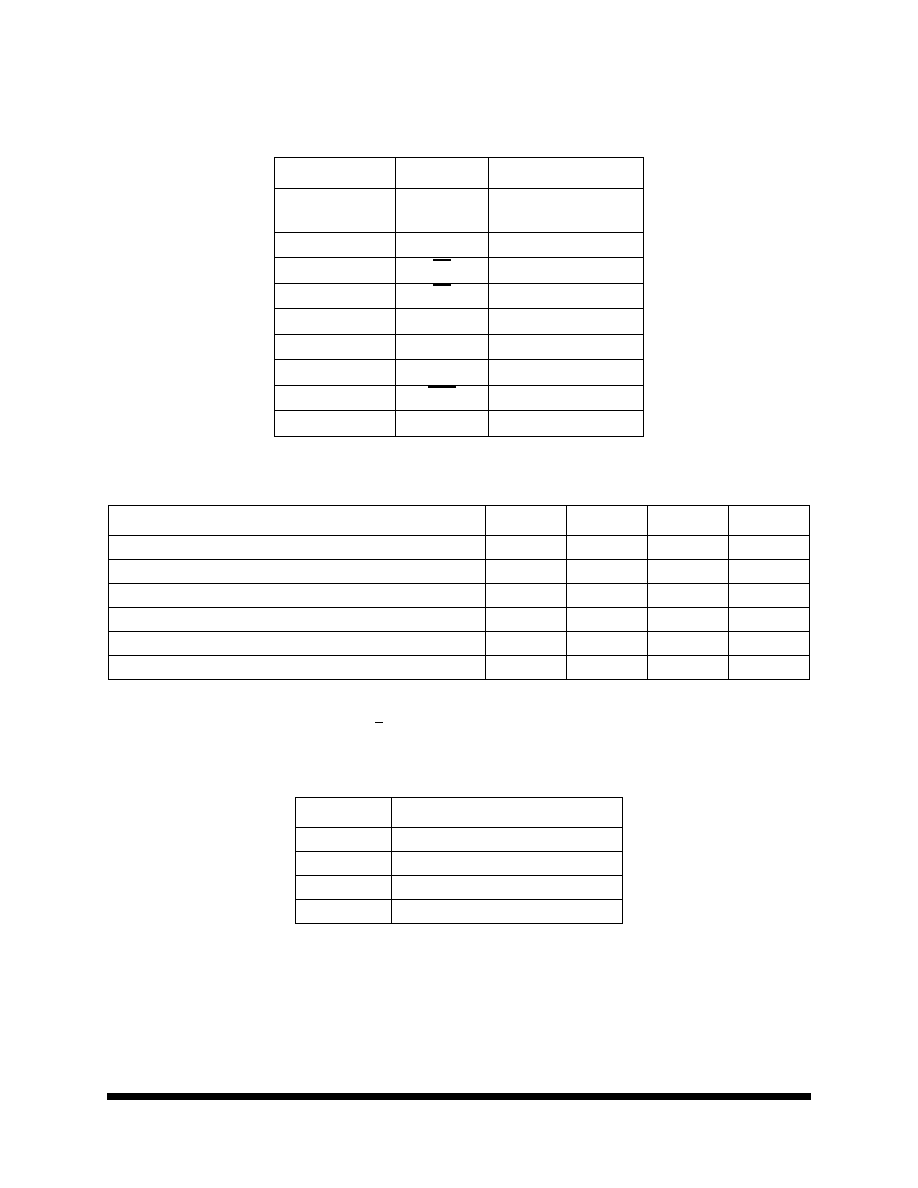
T
ABLE
1. 27C010T P
INOUT
D
ESCRIPTION
P
IN
S
YMBOL
D
ESCRIPTION
12-5, 27, 26, 23, 25,
4, 28, 29, 3 ,2
A0 - A16
Address
I/O0 - I/O7
Input/Output
22
CE
Chip Enable
24
OE
Output Enable
32
V
CC
Power Supply
1
V
PP
Programming Supply
16
V
SS
Ground
31
PGM
Programming Enable
30
NC
No Connection
T
ABLE
2. 27C010T A
BSOLUTE
M
AXIMUM
R
ATINGS
P
ARAMETER
S
YMBOL
M
IN
M
AX
U
NIT
Supply Voltage
1
1. Relative to V
SS
.
V
CC
-0.6
7.0
V
Programming Voltage
1
V
PP
-0.6
13.5
V
All Input and Output Voltage
1,2
2. V
IN
, V
OUT
, and V
ID
min = -1.0V for pulse width < 20 ns.
V
IN
, V
OUT
-0.6
7.0
V
A9 Voltage
2
V
ID
-0.6
13.0
V
Operating Temperature Range
T
A
-55
+125
�
C
Storage Temperature Range
T
S
-65
+150
�
C
T
ABLE
3. D
ELTA
L
IMITS
P
ARAMETER
V
ARIATION
I
CC
1
�10% of value specified on Table 6
I
CC
2
�10% of value specified on Table 6
I
CC
3
�10% of value specified on Table 6
ISB
�10% of value specified on Table 6

Memory
3
All data sheets are subject to change without notice
�2001 Maxwell Technologies
All rights reserved.
1 Megabit (128K x 8-Bit) - OTP EPROM
27C010T
12.12.01 Rev 2
T
ABLE
4. 27C010T R
ECOMMENDED
O
PERATING
C
ONDITIONS
P
ARAMETER
S
YMBOL
M
IN
M
AX
U
NITS
Supply Voltage
V
CC
4.5
5.5
V
Input Voltage
V
IL
-0.3
1
1. V
IL
min = -1.0V for pulse width < 50 ns.
0.8
V
V
IH
2.2
V
CC
+1
2
2. V
IH
max = V
CC
+ 1.5V for pulse width < 20 ns.
Thermal Impedance
JC
--
1.27
�C/W
Operating Temperature Range
T
A
-55
+125
�
C
T
ABLE
5. 27C010T C
APACITANCE
1
1. Guaranteed by design.
P
ARAMETER
S
YMBOL
M
IN
M
AX
U
NIT
Input Capacitance
C
IN
--
10
pF
Output Capacitance
C
OUT
--
15
pF
T
ABLE
6. 27C010T DC E
LECTRICAL
C
HARACTERISTICS
FOR
R
EAD
O
PERATION
(V
CC
= 5V � 10%, V
PP
= V
SS
, T
A
= -55
TO
+125
�
C,
UNLESS
OTHERWISE
SPECIFIED
)
P
ARAMETER
S
YMBOL
T
EST
C
ONDITION
S
UB
G
ROUPS
M
IN
T
YP
M
IN
U
NIT
Input Leakage Current
I
LI
V
IN
= 5.5V
1, 2, 3
--
--
2
�A
Output Leakage Current
I
LO
V
OUT
= 5.5V/0.45V
1, 2, 3
--
--
2
�A
Standby V
CC
Current
I
SB
CE = V
IH
1, 2, 3
--
--
1
mA
Operating V
CC
Current
I
CC1
I
OUT
= 0 mA, CE = V
IL
1, 2, 3
--
--
30
mA
I
CC2
I
OUT
= 0 mA, f = 5 MHz
1, 2, 3
--
--
30
I
CC3
I
OUT
= 0 mA, f = 10 MHz
1, 2, 3
--
--
50
V
PP
Current
I
PP1
V
PP
= 5.5V
1, 2, 3
--
1
20
�A
Input Voltage
V
IH
1, 2, 3
2.2
--
--
V
V
IL
1, 2, 3
--
--
0.8
Output Voltage
V
OH
I
OH
= -400 �A
1, 2, 3
2.4
--
--
V
V
OL
I
OL
= 2.1 mA
1, 2, 3
--
--
0.45

Memory
4
All data sheets are subject to change without notice
�2001 Maxwell Technologies
All rights reserved.
1 Megabit (128K x 8-Bit) - OTP EPROM
27C010T
12.12.01 Rev 2
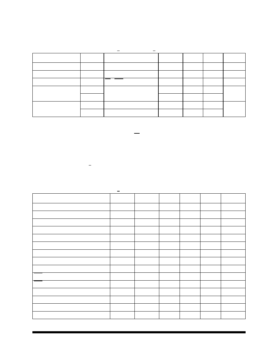
T
ABLE
7. 27C010T AC E
LECTRICAL
C
HARACTERISTICS
FOR
R
EAD
O
PERATION
1
(V
CC
= 5V � 10%, V
PP
= V
SS
, T
A
= -55
TO
+125
�
C,
UNLESS
OTHERWISE
SPECIFIED
)
1. Test conditions:
- Input pulse levels 0.45V/2.4V
- Input rise and fall times
<
10 ns
- Output load 1 TTL gate + 100 pF (including scope and jig)
- Referenced levels for measuring timing 0.8V/2.0V
P
ARAMETER
T
EST
C
ONDITION
S
YMBOL
S
UB
G
ROUPS
M
IN
M
AX
U
NIT
Address Access Time
- 120
- 150
- 200
CE = OE = V
IL
t
ACC
9, 10, 11
--
--
--
120
150
200
ns
Chip Enable Access Time
- 120
- 150
- 200
OE = V
IL
t
CE
9, 10, 11
--
--
--
120
150
200
ns
Output Enable Access TIme
- 120
- 150
- 200
CE = V
IL
t
OE
9, 10, 11
--
--
--
60
70
70
ns
Output Hold to Address Change
- 120
- 150
- 200
CE = V
IL
t
OH
9, 10, 11
0
0
0
--
--
--
ns
Output Disable to High-Z
2
- 120
- 150
- 200
2. t
DF
is defined as the time at which the output becomes an open circuit and data is no longer driven.
CE = OE = V
IL
t
DF
9, 10, 11
0
0
0
50
50
50
ns

Memory
5
All data sheets are subject to change without notice
�2001 Maxwell Technologies
All rights reserved.
1 Megabit (128K x 8-Bit) - OTP EPROM
27C010T
12.12.01 Rev 2
T
ABLE
8. 27C010T DC E
LECTRICAL
C
HARACTERISTICS
FOR
P
ROGRAMMING
O
PERATIONS
1,2,3,4
(V
CC
= 6.25V + 0.25V, V
PP
= 12.5V + 0.3V, T
A
= 25
�
C)
1. V
CC
must be applied before V
PP
and removed after V
PP
.
2. V
PP
must not exceed 13V, inlcuding overshoot.
3. Do not change V
PP
from V
IL
to 12.5V or 12.5V to V
IL
when CE =LOW.
4. DC electrical paramters for programming operations are not tested. These parameters are guaranteed by design.
P
ARAMETER
S
YMBOL
T
EST
C
ONDITION
S
UB
G
ROUPS
M
IN
M
AX
U
NIT
Input Leakage Current
I
LI
V
IN
= 0V to V
CC
1, 2, 3
--
2
�A
Operating V
CC
Current
I
CC
1, 2, 3
--
30
mA
Operating V
PP
Current
I
PP
CE = PGM = V
IL
1, 2, 3
--
40
mA
Input Voltage
5
5. Device reliability may be adversely affected if the device is installed or removed while V
PP
= 12.5V.
V
IH
1, 2, 3
2.2
V
CC
+5
6
6. If V
IH
is over the specified maximum value, programming operation can not be guaranteed.
V
V
IL
1, 2, 3
-0.1
7
7. V
IL
min = -0.6V for pulse width < 20 ns.
0.8
Output Voltage
V
OH
I
OH
= -400 �A
1, 2, 3
2.4
--
V
V
OL
I
OH
= 2.1 mA
1, 2, 3
--
0.45
T
ABLE
9. 27C010T AC E
LECTRICAL
C
HARACTERISTICS
FOR
P
ROGRAMMING
O
PERATIONS
1,2
(V
CC
= 6.25V + 0.25V, V
PP
= 12.5V � 0.3V, T
A
= 25
�
C)
P
ARAMETER
S
YMBOL
S
UB
G
ROUPS
M
IN
T
YP
M
AX
U
NIT
Address Setup Time
t
AS
9, 10, 11
2
--
--
�s
Address Hold Time
t
AH
9, 10, 11
0
--
--
�s
Data Setup Time
t
DS
9, 10, 11
2
--
--
�s
Data Hold Time
t
DH
9, 10, 11
2
--
--
�s
Chip Enable Setup TIme
t
CES
9, 10, 11
2
--
--
�s
V
PP
Setup Time
t
VPS
9, 10, 11
2
--
--
�s
V
CC
Setup Time
t
VCS
9, 10, 11
2
--
--
�s
Output Enable Setup Time
t
OES
9, 10, 11
2
--
--
�s
Output Disable Time
t
DF
9, 10, 11
0
--
130
ns
PGM Initial Programming Pulse Width
t
PW
9, 10, 11
0.19
0.20
0.21
ms
PGM Overprogramming Pulse Width
t
OPW
9, 10, 11
0.19
--
5.25
ms
Data Valid from Output Enable Time
t
OE
9, 10, 11
0
--
150
ns
Output Enable Pulse During Data Latch
t
LW
9, 10, 11
1
--
--
�s
Output Enable Hold Time
t
OEH
9, 10, 11
2
--
--
�s
Chip Enable Hold Time
t
CEH
9, 10, 11
2
--
--
�s
