
1
M
e
m
o
r
y
All data sheets are subject to change without notice
(858) 503-3300- Fax: (858) 503-3301 - www.maxwell.com
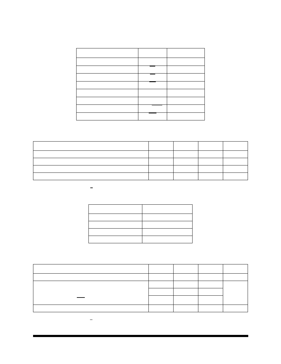
1 Megabit (128K x 8-Bit) EEPROM
28C011T
©2003 Maxwell Technologies
All rights reserved.
11.10.03 REV 10
F
EATURES
:
∑ 128k x 8-bit EEPROM
∑ R
AD
-P
AK
Æ radiation-hardened against natural space radia-
tion
∑ Total dose hardness:
- > 100 krad (Si), depending upon space mission
∑ Excellent Single Event Effects:
- No Latchup > 120 MeV/mg/cm
2
- SEU > 90 MeV/mg/cm
2
read mode
∑ Package:
- 32-pin R
AD
-P
AK
Æ flat package
- 32-pin Rad-Tolerant flat package
- JEDEC-approved byte-wide pinout
∑ High speed:
- 120, 150, and 200 ns maximum access times available
∑ High endurance:
- 10,000 erase/write (in Page Mode),
- 10 year data retention
∑ Page write mode:
- 1 to 128 bytes
∑ Low power dissipation
- 20 mW/MHz active (typical)
- 110 µ W standby (maximum)
D
ESCRIPTION
:
Maxwell Technologies' 28C011T high-density 1 Megabit (128K
x 8-Bit) EEPROM microcircuit features a greater than 100
krad (Si) total dose tolerance, depending upon space mission.
The 28C011T is capable of in-system electrical byte and page
programmability. It has a 128-byte page programming function
to make its erase and write operations faster. It also features
data polling and a Ready/Busy signal to indicate the comple-
tion of erase and programming operations. In the 28C010T,
hardware data protection is provided with the RES pin, in addi-
tion to noise protection on the WE signal and write inhibit on
power on and off. Software data protection is implemented
using the JEDEC optional standard algorithm.
Maxwell Technologies' patented R
AD
-P
AK
Æ packaging technol-
ogy incorporates radiation shielding in the microcircuit pack-
age. It eliminates the need for box shielding while providing
the required radiation shielding for a lifetime in orbit or space
mission. In a GEO orbit, R
AD
-P
AK
Æ provides greater than 100
krad (Si) radiation dose tolerance. This product is available
with screening up to Class S.
High Voltage
Generator
Control Logic Timing
Address
Buffer and
Latch
Y Decoder
X Decoder
Y Gating
Memory Array
I/O Buffer and
Input Latch
Data Latch
V
CC
V
SS
RES
OE
CE
WE
RES
A0
A6
A7
A16
I/O0
I/O7
RDY/Busy
Logic Diagram
28C011T
M
e
m
o
r
y
2
All data sheets are subject to change without notice
©2003 Maxwell Technologies
All rights reserved.
1 Megabit (128K x 8-Bit) EEPROM
28C011T
11.10.03 REV 10
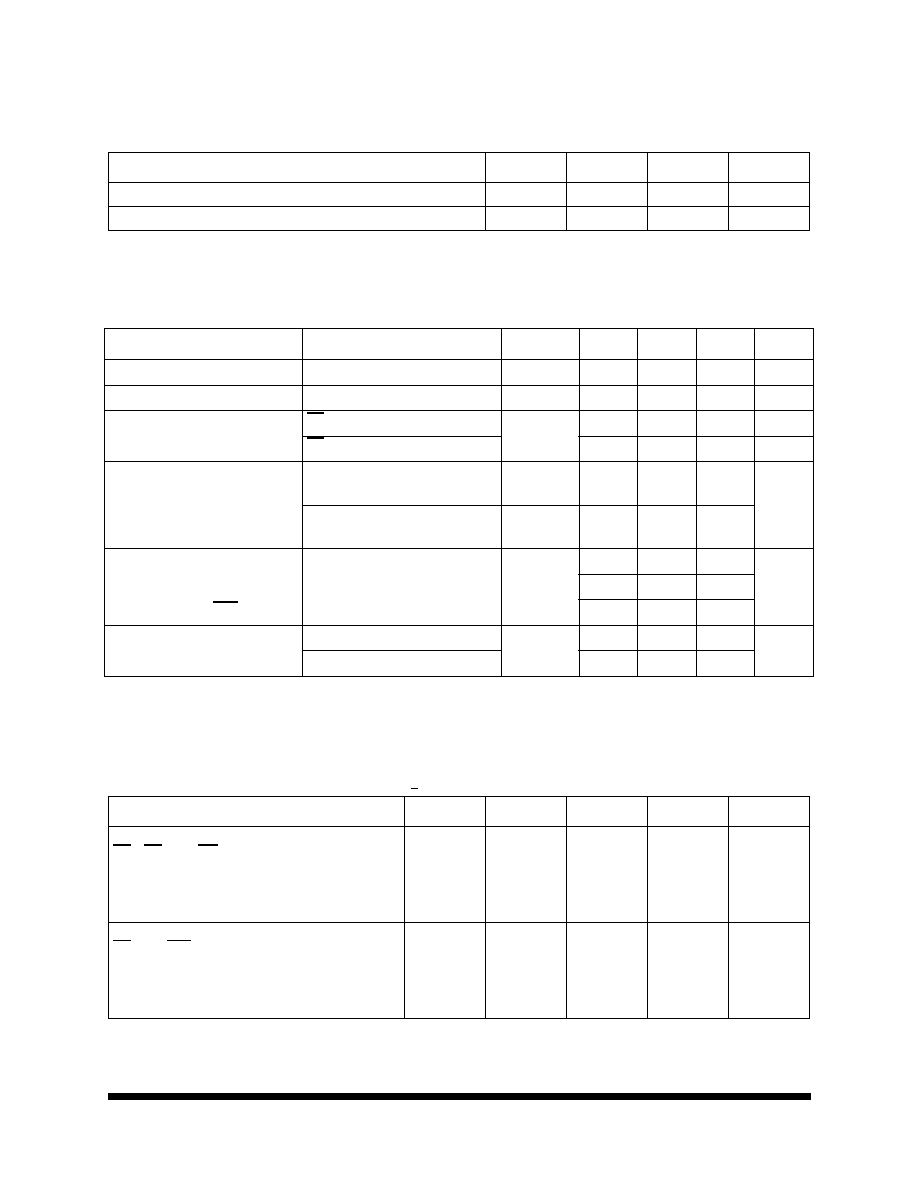
T
ABLE
1. 28C011T P
INOUT
D
ESCRIPTION
P
IN
S
YMBOL
D
ESCRIPTION
12-5, 27, 26, 23, 25, 4, 28, 3, 31, 2
A0-A16
Address
24
OE
Output Enable
22
CE
Chip Enable
29
WE
Write Enable
32
V
CC
Power Supply
16
V
SS
Ground
1
RDY/BUSY
Ready/Busy
30
RES
Reset
T
ABLE
2. 28C011T A
BSOLUTE
M
AXIMUM
R
ATINGS
P
ARAMETER
SYMBOL
MIN
MAX
UNITS
Supply Voltage (Relative to V
SS
)
V
CC
-0.6
+7.0
V
Input Voltage (Relative to V
SS
)
V
IN
-0.5
1
1. V
IN
min = -3.0V for pulse width < 50ns.
+7.0
V
Operating Temperature Range
T
OPR
-55
+125
∞
C
Storage Temperature Range
T
STG
-65
+150
∞
C
T
ABLE
3. D
ELTA
L
IMITS
P
ARAMETER
V
ARIATION
I
CC
1
±10%
I
CC
2
±10%
I
CC
3A
±10%
I
CC
3B
±10%
T
ABLE
4. 28C011T R
ECOMMENDED
O
PERATING
C
ONDITIONS
P
ARAMETER
S
YMBOL
M
IN
M
AX
U
NITS
Supply Voltage
V
CC
4.5
5.5
V
Input Voltage
RES_PIN
V
IL
-0.3
1
1. V
IL
min = -1.0V for pulse width < 50 ns
0.8
V
V
IH
2.2
V
CC
+0.3
V
H
V
CC
-0.5
V
CC
+1
Operating Temperature Range
T
OPR
-55
+125
∞
C
M
e
m
o
r
y
3
All data sheets are subject to change without notice
©2003 Maxwell Technologies
All rights reserved.
1 Megabit (128K x 8-Bit) EEPROM
28C011T
11.10.03 REV 10
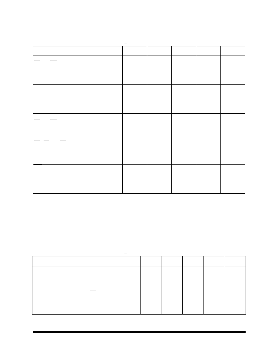
T
ABLE
5. 28C011T C
APACITANCE
(T
A
= 25
∞
C, f = 1 MHZ)
P
ARAMETER
S
YMBOL
M
IN
M
AX
U
NITS
Input Capacitance: V
IN
= 0V
1
C
IN
--
6
pF
Output Capacitance: V
OUT
= 0V
1
C
OUT
--
12
pF
1. Guaranteed by design.
T
ABLE
6. 28C011T DC E
LECTRICAL
C
HARACTERISTICS
(V
CC
= 5V ± 10%, T
A
= -55
TO
+125
∞
C,
UNLESS
OTHERWISE
SPECIFIED
)
P
ARAMETER
T
EST
C
ONDITION
S
UBGROUPS
S
YMBOL
M
IN
M
AX
U
NITS
Input Leakage Current
V
CC
= 5.5V, V
IN
= 5.5V
1, 2, 3
I
IL
--
2
1
µ A
Output Leakage Current
V
CC
= 5.5V, V
OUT
= 5.5V/0.4V
1, 2, 3
I
LO
--
2
µ A
Standby V
CC
Current
CE = V
CC
1, 2, 3
I
CC1
--
20
µ A
CE = V
IH
I
CC2
--
1
mA
Operating V
CC
Current
I
OUT
= 0mA, Duty = 100%, Cycle =
1µ s at V
CC
= 5.5V
1, 2, 3
I
CC3A
--
15
mA
I
OUT
= 0mA, Duty = 100%, Cycle =
150ns at V
CC
= 5.5V
1, 2, 3
I
CC3B
--
50
Input Voltage
RES_PIN
1, 2, 3
V
IL
--
0.8
V
V
IH
2.2
--
V
H
V
CC
-0.5
--
Output Voltage
I
OL
= 2.1 mA
1, 2, 3
V
OL
--
0.4
V
I
OH
= -0.4 mA
V
OH
2.4
--
1. I
LI
on RES = 100 uA max.
T
ABLE
7. 28C011T AC E
LECTRICAL
C
HARACTERISTICS
FOR
R
EAD
O
PERATION
1
(V
CC
= 5V + 10%, T
A
= -55
TO
+125
∞
C)
P
ARAMETER
S
YMBOL
S
UBGROUPS
M
IN
M
AX
U
NITS
Address Access Time
CE = OE = V
IL
, WE = V
IH
-120
-150
-200
t
ACC
9, 10, 11
--
--
--
120
150
200
ns
Chip Enable Access Time
OE = V
IL
, WE = V
IH
-120
-150
-200
t
CE
9, 10, 11
--
--
--
120
150
200
ns
M
e
m
o
r
y
4
All data sheets are subject to change without notice
©2003 Maxwell Technologies
All rights reserved.
1 Megabit (128K x 8-Bit) EEPROM
28C011T
11.10.03 REV 10
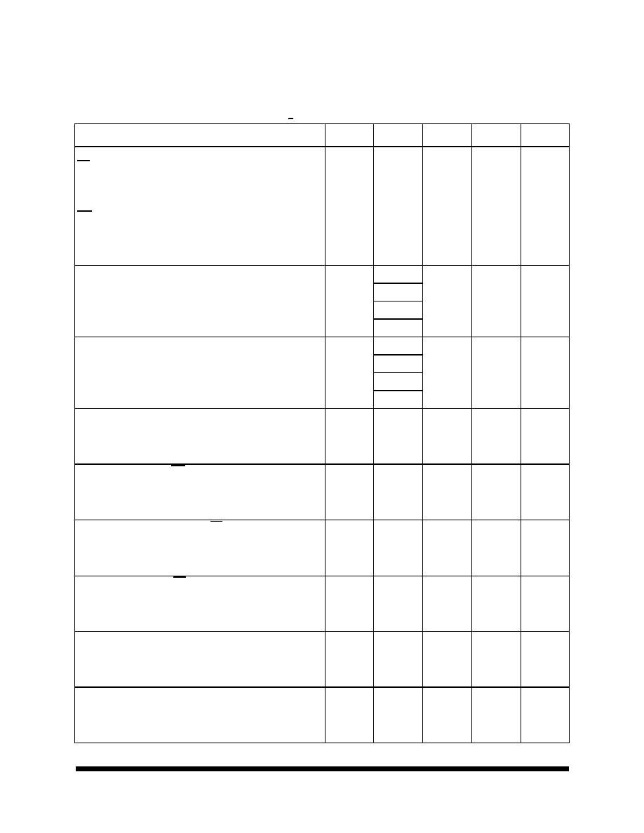
Output Enable Access Time
CE = V
IL
, WE = V
IH
-120
-150
-200
t
OE
9, 10, 11
0
0
0
75
75
100
ns
Output Hold to Address Change
CE = OE = V
IL
, WE = V
IH
-120
-150
-200
t
OH
9, 10, 11
0
0
0
--
--
--
ns
Output Disable to High-Z
2
CE = V
IL
, WE = V
IH
-120
-150
-200
CE = OE = V
IL
, WE = V
IH
-120
-150
-200
t
DF
t
DFR
9, 10, 11
0
0
0
0
0
0
50
50
60
300
350
450
ns
RES to Output Delay
3
CE = OE = V
IL
, WE = V
IH
-120
-150
-200
t
RR
9, 10, 11
--
--
--
400
450
650
ns
1. Test conditions: Input pulse levels - 0.4V to 2.4V; input rise and fall times < 20ns; output load - 1 TTL gate + 100pF (including
scope and jig); reference levels for measuring timing - 0.8V/1.8V.
2. t
DF
and t
DFR
are defined as the time at which the output becomes an open circuit and data is no longer driven.
3. Guaranteed by design.
T
ABLE
8. 28C011T AC E
LECTRICAL
C
HARACTERISTICS
FOR
P
AGE
/B
YTE
E
RASE
AND
B
YTE
W
RITE
O
PERATIONS
(V
CC
= 5V + 10%, T
A
= -55
TO
+125
∞
C)
P
ARAMETER
S
YMBOL
S
UBGROUPS
M
IN
1
M
AX
U
NITS
Address Setup Time
-120
-150
-200
t
AS
9, 10, 11
0
0
0
--
--
--
ns
Chip Enable to Write Setup Time (WE controlled)
-120
-150
-200
t
CS
9, 10, 11
0
0
0
--
--
--
ns
T
ABLE
7. 28C011T AC E
LECTRICAL
C
HARACTERISTICS
FOR
R
EAD
O
PERATION
1
(V
CC
= 5V + 10%, T
A
= -55
TO
+125
∞
C)
P
ARAMETER
S
YMBOL
S
UBGROUPS
M
IN
M
AX
U
NITS
M
e
m
o
r
y
5
All data sheets are subject to change without notice
©2003 Maxwell Technologies
All rights reserved.
1 Megabit (128K x 8-Bit) EEPROM
28C011T
11.10.03 REV 10
Write Pulse Width
CE controlled
-120
-150
-200
WE controlled
-120
-150
-200
t
CW
t
WP
9, 10, 11
200
250
350
200
250
350
--
--
--
--
--
--
ns
Address Hold Time
-120
-150
-200
t
AH
9, 10, 11
150
150
200
--
--
--
ns
Data Setup Time
-120
-150
-200
t
DS
9, 10, 11
75
100
150
--
--
--
ns
Data Hold Time
-120
-150
-200
t
DH
9, 10, 11
10
10
10
--
--
--
ns
Chip Enable Hold Time (WE controlled)
-120
-150
-2000
t
CH
9, 10, 11
0
0
0
--
--
--
ns
Write Enable to Write Setup Time (CE controlled)
-120
-150
-200
t
WS
9, 10, 11
0
0
0
--
--
--
ns
Write Enable Hold Time (CE controlled)
-120
-150
-200
t
WH
9, 10, 11
0
0
0
--
--
--
ns
Output Enable to Write Setup Time
-120
-150
-200
t
OES
9, 10, 11
0
0
0
--
--
--
ns
Output Enable Hold Time
-120
-150
-200
t
OEH
9, 10, 11
0
0
0
--
--
--
ns
T
ABLE
8. 28C011T AC E
LECTRICAL
C
HARACTERISTICS
FOR
P
AGE
/B
YTE
E
RASE
AND
B
YTE
W
RITE
O
PERATIONS
(V
CC
= 5V + 10%, T
A
= -55
TO
+125
∞
C)
P
ARAMETER
S
YMBOL
S
UBGROUPS
M
IN
1
M
AX
U
NITS