1
M
e
m
o
r
y
All data sheets are subject to change without notice
(858) 503-3300 - Fax: (858) 503-3301- www.maxwell.com
256K EEPROM (32K x 8-Bit)
28C256T
©2001 Maxwell Technologies
All rights reserved.
EEPROM
02.18.02 Rev 5
F
EATURES
:
∑ R
AD
-P
AK
Æ radiation-hardened against natural space radia-
tion
∑ Total dose hardness:
- > 100 Krad (Si), dependent upon space mission
∑ Excellent Single Event Effects:
- SEL
TH
LET: > 120 MeV/mg/cm
2
- SEU
TH
LET (read mode): > 90 MeV/mg/cm
2
- SEU
TH
LET (write mode): > 18 MeV/mg/cm
2
∑ Package:
- 28 pin R
AD
-P
AK
Æ flat pack
- 28 pin R
AD
-P
AK
Æ DIP
- JEDEC approved byte wide pinout
∑ High Speed:
- 120, 150 ns maximum access times available
∑ High endurance:
- 10,000 erase/write (in Page Mode), 10-year data
retention
∑ Page Write Mode:
- 1 to 64 bytes
∑ Low power dissipation:
- 15 mA active current (cycle = 1 µ s)
- 20 µ A standby current (CE = V
CC
)
D
ESCRIPTION
:
Maxwell Technologies' 28C256T high density 256k-bit
EEPROM microcircuit features a greater than 100 krad (Si)
total dose tolerance, depending upon space mission. The
28C256T is capable of in-system electrical byte and page pro-
grammability. It has a 64-Byte page programming function to
make its erase and write operations faster. It also features
data polling to indicate the completion of erase and program-
ming operations.
Maxwell Technologies' patented R
AD
-P
AK
Æ packaging technol-
ogy incorporates radiation shielding in the microcircuit pack-
age. It eliminates the need for box shielding while providing
the required radiation shielding for a lifetime in orbit or space
mission. In a GEO orbit, R
AD
-P
AK
provides greater than 100
krad (Si) radiation dose tolerance. This product is available
with screening up to Class S.
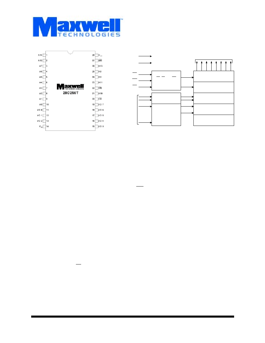
OE, CE, and WE
LOGIC
Y DECODER
X DECODER
DATA LATCH
INPUT/OUTPUT
BUFFERS
Y-GATING
CELL MATRIX
IDENTIFICATION
OE
WE
CE
ADDRESS
INPUTS
V
CC
GND
DATA INPUTS/OUTPUTS
I/O0 - I/O7
Logic Diagram

M
e
m
o
r
y
2
All data sheets are subject to change without notice
©2001 Maxwell Technologies
All rights reserved.
256K EEPROM (32K x 8-Bit) EEPROM
28C256T
02.18.02 Rev5
*Refer to diagram on Page 1 for pin relationship.
T
ABLE
1. 28C256T P
INOUT
D
ESCRIPTION
P
IN
S
YMBOL
D
ESCRIPTION
*10-3, 25, 24,
21, 23, 2, 26, 1
A0-A14
Address
11-13, 15-19
I/O0-I/O7
Input/Output
22
OE
Output Enable
20
CE
Chip Enable
27
WE
Write Enable
28
V
CC
Power Supply
14
V
SS
Ground
T
ABLE
2. 28C256T A
BSOLUTE
M
AXIMUM
R
ATINGS
P
ARAMETER
S
YMBOL
M
IN
M
AX
U
NITS
Supply Voltage (Relative to V
SS
)
V
CC
-0.6
7.0
V
Input Voltage (Relative to V
SS
)
V
IN
-0.5
1
1. V
IN
= -3.0 V for pulse width > 50 ns.
7.0
V
Operating Temperature Range
2
2. Including electrical characteristics and data retention.
T
OPR
-55
125
∞
C
Storage Temperature Range
T
STG
-65
150
∞
C
T
ABLE
3. 28C256T D
ELTA
L
IMITS
P
ARAMETER
V
ARIATION
I
CC
1
±10%
I
CC
2
±10%
I
CC
3A
±10%
I
CC
3B
±10%
M
e
m
o
r
y
3
All data sheets are subject to change without notice
©2001 Maxwell Technologies
All rights reserved.
256K EEPROM (32K x 8-Bit) EEPROM
28C256T
02.18.02 Rev5
T
ABLE
4. 28C256T R
ECOMMENDED
O
PERATING
C
ONDITIONS
P
ARAMETER
S
UBGROUPS
S
YMBOL
M
IN
M
AX
U
NITS
Supply Voltage
1
V
CC
4.5
5.5
V
Input Voltage
1
V
IL
V
IH
V
H
-0.3
1
2.2
V
CC
-0.5
1. V
IL
min= -1.0V for pulse width < 50 ns.
0.8
V
CC
+0.3
V
CC
+1
V
V
V
1
1
Thermal Impedance -- Flat Package
1
JC
--
0.87
∞C/W
Thermal Impedance -- DIP Package
1
JC
--
0.86
∞C/W
Operating Temperature Range
1
T
OPR
-55
125
∞
C
T
ABLE
5. 28C256T C
APACITANCE
1
(T
A
= 25
∞
C, f = 1 MHz)
P
ARAMETER
S
YMBOL
M
IN
M
AX
U
NITS
Input Capacitance: V
IN
= 0V
1
1. Guaranteed by design.
C
IN
--
6
pF
Output Capacitance: V
OUT
= 0V
1
C
OUT
--
12
pF
T
ABLE
6. 28C256T DC E
LECTRICAL
C
HARACTERISTICS
(V
CC
= 5 V ± 10%, T
A
= -55
TO
+125
∞
C
UNLESS
OTHERWISE
SPECIFIED
)
P
ARAMETER
C
ONDITIONS
S
UBGROUPS
S
YMBOL
M
IN
M
AX
U
NITS
Input Leakage Current
V
CC
= 5.5 V, V
IN
= 5.5 V
1, 2, 3
I
LI
--
2
uA
Output Leakage Current
V
CC
= 5.5 V, V
OUT
= 5.5 V/0.4 V
1, 2, 3
I
LO
--
2
uA
Standby V
CC
Current
CE = V
CC
1, 2, 3
I
CC1
--
20
uA
CE = V
IH
1, 2, 3
I
CC2
--
1
mA
Operating V
CC
Current
I
OUT
= 0 mA Duty = 100%
V
CC
= 5.5 V Cycle = 1 us
1, 2, 3
I
CC3
--
15
mA
I
OUT
= 0mA Duty = 100%
V
CC
= 5.5 V Cycle = 150 ns
--
50
Input Low Voltage
1, 2, 3
V
IL
--
0.8
V
Input High Voltage
1, 2, 3
V
IH
2.2
--
V
1, 2, 3
V
H
V
CC
-0.5
--
V
Output Low Voltage
I
LO
= 2.1 mA
1, 2, 3
V
OL
--
0.4
V
Output High Voltage
I
OH
= -400 uA
1, 2, 3
V
OH
2.4
--
V
M
e
m
o
r
y
4
All data sheets are subject to change without notice
©2001 Maxwell Technologies
All rights reserved.
256K EEPROM (32K x 8-Bit) EEPROM
28C256T
02.18.02 Rev5
T
ABLE
7. 28C256T AC E
LECTRICAL
C
HARACTERISTICS
FOR
R
EAD
O
PERATION1
(V
CC
= 5V ±10%, T
A
= -55
TO
125 ∞C
UNLESS
OTHERWISE
SPECIFIED
)
1. Test conditions: Input pulse levels - 0V to 3V; input rise and fall times < 20 ns; output load - 1 TTL gate + 100 pF (including scope and jig); ref-
erence levels for measuring timing - 0.8V/1.8V.
P
ARAMETER
S
UBGROUPS
S
YMBOL
M
IN
M
AX
U
NITS
Address Access Time CE = OE = V
IL
, WE = V
IH
-120
-150
9, 10, 11
t
ACC
--
--
120
150
ns
CE to Output Delay OE = V
IL
, WE = V
IH
-120
-150
9, 10, 11
t
CE
--
--
120
150
ns
OE to Output Delay CE = V
IL
, WE = V
IH
-120
-150
9, 10, 11
t
OE
0
0
75
75
ns
Output Hold from Address CE = OE = V
IL
, WE = V
IH
-120
-150
9, 10, 11
t
OH
0
0
--
--
ns
OE (CE) High to Output Float CE = V
IL
, WE = V
IH
2
-120
-150
2. t
DF
and t
DFR
are defined as the time at which the output becomes an open circuit and data is no longer driven.
9, 10, 11
t
DF
0
0
50
50
ns
T
ABLE
8. 28C256T AC E
LECTRICAL
C
HARACTERISTICS
FOR
P
AGE
/B
YTE
E
RASE
AND
W
RITE
O
PERATIONS
(V
CC
= 5V ±10%, T
A
= -55
TO
125 ∞C
UNLESS
OTHERWISE
SPECIFIED
)
P
ARAMETER
S
UBGROUPS
S
YMBOL
M
IN1
T
YP
M
AX
U
NITS
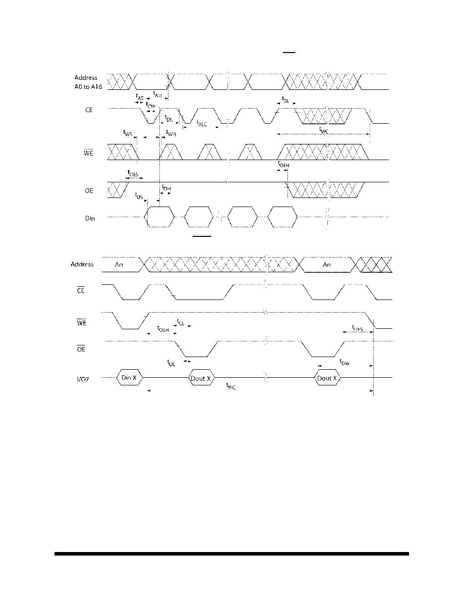
Address Setup Time
-120
-150
t
AS
0
0
--
--
--
--
ns
9, 10, 11
9, 10, 11
CE to Write Setup Time
-120
-150
t
CS
2
0
0
--
--
--
--
ns
9, 10, 11
9, 10, 11
WE to Write Setup Time
-120
-150
t
WS
3
0
0
--
--
--
--
ns
9, 10, 11
9, 10, 11
WE Hold Time
-120
-150
9, 10, 11
t
WH
3
0
0
--
--
ns

M
e
m
o
r
y
5
All data sheets are subject to change without notice
©2001 Maxwell Technologies
All rights reserved.
256K EEPROM (32K x 8-Bit) EEPROM
28C256T
02.18.02 Rev5
WE Pulse Width
-120
-150
CE Pulse Width
-120
-150
9, 10, 11
t
WP
2
t
CW
3
200
250
200
250
--
--
--
--
--
--
--
--
ns
Address Hold Time
-120
-150
9, 10, 11
t
AH
150
150
--
--
--
--
ns
Data Setup Time
-120
-150
9, 10, 11
t
DS
75
100
--
--
--
--
ns
Data Hold Time
-120
-150
9, 10, 11
t
DH
10
10
--
--
--
--
ns
Chip Enable Hold Time
2
-120
-150
9, 10, 11
t
CH
0
0
--
--
--
--
ns
Output Enable to Write Setup Time
-120
-150
9, 10, 11
t
OES
0
0
--
--
--
--
ns
Output Enable Hold Time
-120
-150
9, 10, 11
t
OEH
0
0
--
--
--
--
ns
Data Latch Time
4
-120
-150
9, 10, 11
t
DL
--
--
230
280
--
--
ns
Write Cycle Time
-120
-150
9, 10, 11
t
WC
--
--
--
--
10
10
ms
Byte Load Window
4
-120
-150
9, 10, 11
t
BL
--
--
100
100
--
--
us
Byte Load Cycle
4
-120
-150
9, 10, 11
t
BLC
0.55
0.55
--
--
30
30
us
Write Start Time
-120
-150
9, 10, 11
t
DW
150
150
--
--
--
--
ns
1. Use this device in a longer cycle than this value.
2. WE controlled operation.
3. CE controlled operation.
4. Not tested.
T
ABLE
8. 28C256T AC E
LECTRICAL
C
HARACTERISTICS
FOR
P
AGE
/B
YTE
E
RASE
AND
W
RITE
O
PERATIONS
(V
CC
= 5V ±10%, T
A
= -55
TO
125 ∞C
UNLESS
OTHERWISE
SPECIFIED
)
P
ARAMETER
S
UBGROUPS
S
YMBOL
M
IN1
T
YP
M
AX
U
NITS

M
e
m
o
r
y
6
All data sheets are subject to change without notice
©2001 Maxwell Technologies
All rights reserved.
256K EEPROM (32K x 8-Bit) EEPROM
28C256T
02.18.02 Rev5
T
ABLE
9. 28C256T M
ODE
S
ELECTION
1
M
ODE
CE
OE
WE
I/O
Write
V
IL
V
IL
V
IH
D
OUT
Standby
V
H
X
X
HIGH-Z
Write
V
IL
V
IH
V
IL
D
IN
Deselect
V
IL
V
IH
V
IH
HIGH-Z
Write Inhibit
X
X
V
IH
--
X
V
IL
X
--
Data\ Polling
V
IL
V
IL
V
IH
DATA-OUT
(I/O7)
1. X = Does not matter.
M
e
m
o
r
y
7
All data sheets are subject to change without notice
©2001 Maxwell Technologies
All rights reserved.
256K EEPROM (32K x 8-Bit) EEPROM
28C256T
02.18.02 Rev5
F
IGURE
1. R
EAD
T
IMING
W
AVEFORM
F
IGURE
2. B
YTE
W
RITE
T
IMING
W
AVEFORM
(1) (WE C
ONTROLLED
)

M
e
m
o
r
y
8
All data sheets are subject to change without notice
©2001 Maxwell Technologies
All rights reserved.
256K EEPROM (32K x 8-Bit) EEPROM
28C256T
02.18.02 Rev5
F
IGURE
3. B
YTE
W
RITE
T
IMING
W
AVEFORM
(2) (CE C
ONTROLLED
)
F
IGURE
4. P
AGE
W
RITE
T
IMING
W
AVEFORM
(1) (WE C
ONTROLLED
)
M
e
m
o
r
y
9
All data sheets are subject to change without notice
©2001 Maxwell Technologies
All rights reserved.
256K EEPROM (32K x 8-Bit) EEPROM
28C256T
02.18.02 Rev5
F
IGURE
5. P
AGE
W
RITE
T
IMING
W
AVEFORM
(2) (CE C
ONTROLLED
)
F
IGURE
6. D
ATA
P
OLLING
T
IMING
W
AVEFORM
M
e
m
o
r
y
10
All data sheets are subject to change without notice
©2001 Maxwell Technologies
All rights reserved.
256K EEPROM (32K x 8-Bit) EEPROM
28C256T
02.18.02 Rev5
EEPROM A
PPLICATION
N
OTES
This application note describes the programming procedures for the EEPROM modules and the details of various
techniques to preserve data protection.
Automatic Page Write
Page-mode write feature allows 1 to 64 bytes of data to be written into the EEPROM in a single write cycle, and allows
the undefined data within 64 bytes to be written corresponding to the undefined address (A0 to A5). Loading the first
byte of data, the data load window opens 30 µ s for the second byte. In the same manner each additional byte of data
can be loaded within 30 µ s. In case CE and WE are kept high for 100(s after data input, EEPROM enters erase and
write mode automatically and only the input data are written into the EEPROM.
WE CE Pin Operation
During a write cycle, addresses are latched by the falling edge of WE or CE, and data is latched by the rising edge of
WE or CE.
Data Polling
Data Polling function allows the status of the EEPROM to be determined. If EEPROM is set to read mode during a
write cycle, an inversion of the last byte of data to be loaded outputs from I/O 7 to indicate that the EEPROM is per-
forming a write operation.
Data Protection
To protect the data during operation and power on/off, the EEPROM has the internal functions described below.
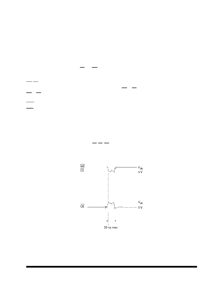
1. Data Protection against Noise of Control Pins (CE, OE, WE) during Operation.
During readout or standby, noise on the control pins may act as a trigger and turn the EEPROM to programming mode by mis-
take. To prevent this phenomenon, the EEPROM has a noise cancellation function that cuts noise if its width is 20ns or less in
programming mode. Be careful not to allow noise of a width of more than 20ns on the control pins.

M
e
m
o
r
y
11
All data sheets are subject to change without notice
©2001 Maxwell Technologies
All rights reserved.
256K EEPROM (32K x 8-Bit) EEPROM
28C256T
02.18.02 Rev5
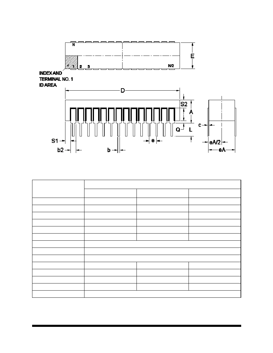
F28-03
Note: All dimensions in inches.
28 P
IN
R
AD
-P
AK
Æ F
LAT
P
ACKAGE
S
YMBOL
D
IMENSION
M
IN
N
OM
M
AX
A
0.165
0.177
0.189
b
0.015
0.017
0.022
c
0.003
0.005
0.009
D
--
0.720
0.740
E
0.380
0.410
0.420
E1
--
--
0.440
E2
0.180
0.240
--
E3
0.030
0.085
--
e
0.050 BSC
L
0.390
0.400
0.410
Q
0.040
0.050
0.053
S1
0.005
0.027
--
N
28
M
e
m
o
r
y
12
All data sheets are subject to change without notice
©2001 Maxwell Technologies
All rights reserved.
256K EEPROM (32K x 8-Bit) EEPROM
28C256T
02.18.02 Rev5
D28-03
Note: All dimensions in inches.
28 P
IN
R
AD
-P
AK
Æ D
UAL
I
N
L
INE
P
ACKAGE
S
YMBOL
D
IMENSION
M
IN
N
OM
M
AX
A
--
0.177
0.225
b
0.014
0.018
0.026
b2
0.045
0.050
0.065
c
0.008
0.010
0.018
D
--
1.400
1.485
E
0.510
0.595
0.620
eA
0.600 BSC
eA/2
0.300 BSC
e
0.100 BSC
L
0.140
0.150
0.160
Q
0.015
0.040
0.060
S1
0.005
0.025
--
S2
0.005
--
--
N
28

M
e
m
o
r
y
13
All data sheets are subject to change without notice
©2001 Maxwell Technologies
All rights reserved.
256K EEPROM (32K x 8-Bit) EEPROM
28C256T
02.18.02 Rev5
Important Notice:
These data sheets are created using the chip manufacturer's published specifications. Maxwell Technologies verifies
functionality by testing key parameters either by 100% testing, sample testing or characterization.
The specifications presented within these data sheets represent the latest and most accurate information available to
date. However, these specifications are subject to change without notice and Maxwell Technologies assumes no
responsibility for the use of this information.
Maxwell Technologies' products are not authorized for use as critical components in life support devices or systems
without express written approval from Maxwell Technologies.
Any claim against Maxwell Technologies must be made within 90 days from the date of shipment from Maxwell Tech-
nologies. Maxwell Technologies' liability shall be limited to replacement of defective parts.

M
e
m
o
r
y
14
All data sheets are subject to change without notice
©2001 Maxwell Technologies
All rights reserved.
256K EEPROM (32K x 8-Bit) EEPROM
28C256T
02.18.02 Rev5
Product Ordering Options
Model Number
Feature
Option Details
28C256T
XX
X
X
-XX
Access Time
Screening Flow
Package
Radiation Feature
Base Product
Nomenclature
12 = 120 ns
15 = 150 ns
Monolithic
S = Maxwell Class S
B = Maxwell Class B
E = Engineering (testing @ +25∞C)
I = Industrial (testing @ -55∞C,
+25∞C, +125∞C)
D = Dual In-line Package (DIP)
F = Flat Pack
RP = R
AD
-P
AK
Æ package
RT1 = Guaranteed to 10 krad at
die level
RT2 = Guaranteed to 25 krad at
die level
RT4 = Guaranteed to 40 krad at
die level
256K EEPROM (32K x 8-Bit)
EEPROM