1
M
e
m
o
r
y
All data sheets are subject to change without notice
(858) 503-3300 - Fax: (858) 503-3301- www.maxwell.com
3.3V 1 Megabit (128K x 8-Bit)
28LV011
©2002 Maxwell Technologies
All rights reserved.
EEPROM
05.28.02 Rev 2
F
EATURES
:
∑ 3.3V low voltage operation 128K x 8 Bit EEPROM
∑ R
AD
-P
AK
Æ radiation-hardened against natural space
radiation
∑ Total dose hardness:
- > 100 krad (Si), depending upon space mission
∑ Excellent Single Event Effects:
- SEL
TH
> 84 MeV/mg/cm
2
- SEU
TH
> 37 Mev/mg/cm
2
(read mode)
- SEU saturated cross section = 3E-6 cm
2
(read mode)
- SEU
TH
= 11.4 Mev/mg/cm
2
(write mode)
- SEU saturated cross section = 5E-3 cm
2
(write mode)
with hard errors
∑ Package:
- 32 Pin R
AD
-P
AK
Æ flat pack
- 32 Pin R
AD
-P
AK
Æ DIP
- JEDEC-approved byte-wide pinout
∑ Address Access Time:
- 200, 250 ns Access times available
∑ High endurance:
- 10,000 erase/write (in Page Mode), 10-year data
retention
∑ Page write mode:
- 1 to 128 bytes
∑ Automatic programming
- 15 ms automatic page/byte write
∑ Low power dissipation
- 20 mW/MHz active current (typ.)
- 72 µ W standby (maximum)
D
ESCRIPTION
:
Maxwell Technologies' 28LV011 high density, 3.3V, 1 Megabit
EEPROM microcircuit features a greater than 100 krad (Si)
total dose tolerance, depending upon space mission. The
28LV011 is capable of in-system electrical Byte and Page pro-
grammability. It has a 128-Byte Page Programming function to
make its erase and write operations faster. It also features
Data Polling and a Ready/Busy signal to indicate the comple-
tion of erase and programming operations. In the 28LV011,
hardware data protection is provided with the RES pin, in addi-
tion to noise protection on the WE signal and write inhibit on
power on and off. Meanwhile, software data protection is
implemented using the JEDEC-optional Standard algorithm.
The 28LV011 is designed for high reliability in the most
demanding space applications.
Maxwell Technologies' patented R
AD
-P
AK
Æ packaging technol-
ogy incorporates radiation shielding in the microcircuit pack-
age. It eliminates the need for box shielding while providing
the required radiation shielding for a lifetime in orbit or space
mission. In a GEO orbit, R
AD
-P
AK
Æ provides greater than 100
krad (Si) radiation dose tolerance. This product is available
with screening up to Class S.
Note:The recommended form of data protection during power
on/off is to hold the RES pin to V
SS
during power up and power
down. This may be accompanied by connecting the RES pin
to the CPU reset line. Failure to provide adequate protection
during power on/off may result in lost or modified data.
High Voltage
Generator
Control Logic Timing
Address
Buffer and
Latch
Y Decoder
X Decoder
Y Gating
Memory Array
I/O Buffer and
Input Latch
Data Latch
V
CC
V
SS
RES
OE
CE
WE
RES
A0
A6
A7
A16
I/O0
I/O7
RDY/Busy
Logic Diagram
28LV011
M
e
m
o
r
y
2
All data sheets are subject to change without notice
©2002 Maxwell Technologies
All rights reserved.
3.3V 1 Megabit (128K x 8-Bit) EEPROM
28LV011
05.28.02 Rev 2
T
ABLE
1. 28LV011A P
INOUT
D
ESCRIPTION
P
IN
S
YMBOL
D
ESCRIPTION
12-5, 27, 26, 23, 25,
4, 28, 3, 31, 2
A0-A16
Address
13-15, 17-21
I/O0 - I/O7
Input/Output
24
OE
Output Enable
22
CE
Chip Enable
29
WE
Write Enable
32
V
CC
Power Supply
16
V
SS
Ground
1
RDY/BUSY
Ready/Busy
30
RES
Reset
T
ABLE
2. 28LV011 A
BSOLUTE
M
AXIMUM
R
ATINGS
P
ARAMETER
S
YMBOL
M
IN
M
AX
U
NIT
Supply Voltage (Relative to Vss)
V
CC
-0.6
7.0
V
Input Voltage (Relative to Vss)
V
IN
-0.5
1
1. V
IN
min = -3.0 V for pulse width < 50 ns.
7.0
V
Operating Temperature Range
T
OPR
-55
125
∞C
Storage Temperature Range
T
STG
-65
150
∞C
T
ABLE
3. D
ELTA
L
IMITS
P
ARAMETER
V
ARIATION
I
CC
1
±10%
I
CC
2
±10%
I
CC
3A
±10%
I
CC
3B
±10%

M
e
m
o
r
y
3
All data sheets are subject to change without notice
©2002 Maxwell Technologies
All rights reserved.
3.3V 1 Megabit (128K x 8-Bit) EEPROM
28LV011
05.28.02 Rev 2
T
ABLE
4. 28LV011 R
ECOMMENDED
O
PERATING
C
ONDITIONS
P
ARAMETER
SYMBOL
MIN
MAX
UNIT
Supply Voltage
V
CC
3.0
3.6
V
Input Voltage
RES_PIN
V
IL
V
IH
V
H
-0.3
1
2.0
2
V
CC
-0.5
1. V
IL
min = -1.0 V for pulse width < 50 ns.
2. V
IH
min = 2.2 V for V
CC
= 3.6 V.
0.8
V
CC
+0.3
V
CC
+1
V
Operating Temperature Range
T
OPR
-55
+125
∞C
T
ABLE
5. 28LV011 C
APACITANCE
(T
A
= 25∞C, F = 1MH
Z
)
P
ARAMETER
S
YMBOL
M
IN
M
AX
U
NIT
Input Capacitance: V
IN
= 0V
1
1. Guaranteed by design.
C
IN
--
6 pF
Output Capacitance: V
OUT
= 0V
1
C
OUT
--
12 pF
T
ABLE
6. 28LV011 DC E
LECTRICAL
C
HARACTERISTICS
(V
CC
= 3.3V ± 0.3, T
A
= -55
TO
+125∞C
UNLESS
OTHERWISE
SPECIFIED
)
P
ARAMETER
T
EST
C
ONDITIONS
S
UBGROUPS
S
YMBOL
M
IN
M
AX
U
NIT
Input Leakage Current V
CC
= 3.6V, V
IN
= 3.6V
1, 2, 3
I
LI
--
2
µ A
Output Leakage Cur-
rent
V
CC
= 3.6V, V
OUT
= 3.6V/0.4V
1, 2, 3
I
LO
--
2
µ A
Standby V
CC
Current
CE = V
CC
CE = V
IH
1, 2, 3
I
CC1
I
CC2
--
--
20
1
µ A
mA
Operating V
CC
Current I
OUT
= 0mA, Duty = 100%, Cycle = 1 µ s
@ V
CC
= 3.3V
I
OUT
= 0mA, Duty = 100%, Cycle = 250 ns @ V
CC
=
3.3V
1, 2, 3
I
CC3
--
--
6
15
mA
Input Voltage
1, 2, 3
V
IL
V
IH
V
H
--
2.0
1
V
CC
-0.5
1. V
IH
min = 2.2V for V
CC
= 3.6V.
0.8
--
--
V
Output Voltage
I
OL
= 2.1 mA
I
OH
= -400 µ A
1, 2, 3
V
OL
V
OH
--
V
CC
x0.8
0.4
--
V

M
e
m
o
r
y
4
All data sheets are subject to change without notice
©2002 Maxwell Technologies
All rights reserved.
3.3V 1 Megabit (128K x 8-Bit) EEPROM
28LV011
05.28.02 Rev 2
T
ABLE
7. 28LV011 AC C
HARACTERISTICS
FOR
R
EAD
O
PERATION1
(V
CC
= 3.3V ± 10%, T
A
= -55
TO
+125 ∞C
UNLESS
OTHERWISE
SPECIFIED
)
1. Test conditions: Input pulse levels - 0.4V to 2.4V; input rise and fall times < 20 ns; output load - 1 TTL gate + 100 pF (including
scope and jig); reference levels for measuring timing - 0.8V/1.8V.
P
ARAMETER
T
EST
C
ONDITIONS
S
UBGROUPS
S
YMBOL
M
IN
M
AX
U
NIT
Functional Test
Verify Truth Table
7, 8A, 8B
All
Address Access Time
-200
-250
CE = OE = V
IL
, WE = V
IH
9, 10, 11
t
ACC
--
--
200
250
ns
Chip Enable Access Time
-200
-250
OE = V
IL
, WE = V
IH
9, 10, 11
t
CE
--
--
200
250
ns
Output Enable Access Time
-200
-250
CE = V
IL
, WE = V
IH
9, 10, 11
t
OE
0
0
110
120
ns
Output Hold to Address Change
-200
-250
CE = OE = V
IL
, WE = V
IH
9, 10, 11
t
OH
0
0
--
--
ns
Output Disable to High-Z
2
-200
-250
2. t
DF
and t
DFR
is defined as the time at which the output becomes an open circuit and data is no longer driven.
CE = V
IL
, WE = V
IH
CE = OE = V
IL
, WE = V
IH
9, 10, 11
t
DF
0
0
50
50
ns
Output Disable to High-Z
-200
-250
CE = V
IL
, WE = V
IH
CE = OE = V
IL
, WE = V
IH
9, 10, 11
t
DFR
0
0
300
350
ns
RES to Output Delay
3
-200
-250
3. Guaranteed by design.
CE = OE = V
IL
WE = V
IH
9, 10, 11
t
RR
0
0
525
550
ns

M
e
m
o
r
y
5
All data sheets are subject to change without notice
©2002 Maxwell Technologies
All rights reserved.
3.3V 1 Megabit (128K x 8-Bit) EEPROM
28LV011
05.28.02 Rev 2
T
ABLE
8. 28LV011 AC E
LECTRICAL
C
HARACTERISTICS
FOR
E
RASE
AND
W
RITE
O
PERATIONS
(V
CC
= 3.3V ± 10%, T
A
= -55
TO
+125 ∞C
UNLESS
OTHERWISE
SPECIFIED
)
P
ARAMETER
S
UBGROUPS
S
YMBOL
M
IN
M
AX
U
NIT
Address Setup Time
-200
-250
9, 10, 11
t
AS
0
0
--
--
ns
Chip Enable to Write Setup Time (WE controlled)
-200
-250
9, 10, 11
t
CS
0
0
--
--
ns
Write Pulse Width (CE controlled)
-200
-250
9, 10, 11
t
CW
200
250
--
--
ns
Write Pulse Width (WE controlled)
-200
-250
9, 10, 11
t
WP
200
250
--
--
ns
Address Hold Time
-200
-250
9, 10, 11
t
AH
125
150
--
--
ns
Data Setup Time
-200
-250
9, 10, 11
t
DS
100
100
--
--
ns
Data Hold Time
-200
-250
9, 10, 11
t
DH
10
10
--
--
ns
Chip Enable Hold Time (WE controlled)
-200
-250
9, 10, 11
t
CH
0
0
--
--
ns
Write Enable to Write Setup Time (CE controlled)
-200
-250
9, 10, 11
t
WS
0
0
--
--
ns
Write Enable Hold Time (CE controlled)
-200
-250
9, 10, 11
t
WH
0
0
--
--
ns
Output Enable to Write Setup Tim
-200
-250
9, 10, 11
t
OES
0
0
--
--
ns
Output Enable Hold Time
-200
-250
9, 10, 11
t
OEH
0
0
--
--
ns
Write Cycle Time
1,2
-200
-250
9, 10, 11
t
WC
--
--
15
15
ms

M
e
m
o
r
y
6
All data sheets are subject to change without notice
©2002 Maxwell Technologies
All rights reserved.
3.3V 1 Megabit (128K x 8-Bit) EEPROM
28LV011
05.28.02 Rev 2
Byte Load Cycle
-200
-250
9, 10, 11
t
BLC
1
1
30
30
µ s
Data Latch Time
2
-200
-250
9, 10, 11
t
DL
700
750
--
--
ns
Byte Load Window
2
-200
-250
9, 10, 11
t
BL
100
100
--
--
µ s
Time to Device Busy
-200
-250
9, 10, 11
t
DB
100
120
--
--
ns
Write Start Time
-200
-250
9, 10, 11
t
DW
250
250
--
--
ns
RES to Write Setup Time
2
-200
-250
9, 10, 11
t
RP
100
100
--
--
µ s
V
CC
to RES Setup Time
2
-200
-250
9, 10, 11
t
RES
1
1
--
--
µ s
1. t
WC
must be longer than this value unless polling techniques or RDY/BSY are used. This device automatically completes the
internal write operation within this value.
2. Guaranteed by design.
T
ABLE
9. 28LV011 M
ODE
S
ELECTION1,2
M
ODE
CE
OE
WE
RES
RDY/BUSY
I/O
Read
V
IL
V
IL
V
IH
V
H
High-Z
D
OUT
Standby
V
IH
X
X
X
High-Z
High-Z
Write
V
IL
V
IH
V
IL
V
H
High-Z --> V
OL
D
IN
Deselect
V
IL
V
IH
V
IH
V
H
High-Z
High-Z
Write Inhibit
X
X
V
IH
X
--
--
X
V
IL
X
X
--
--
Data Polling
V
IL
V
IL
V
IH
V
H
V
OL
Data Out (I/O7)
Program
X
X
X
V
IL
High-Z
High-Z
1. X = Don't care.
2. Refer to the recommended DC operating conditions.
T
ABLE
8. 28LV011 AC E
LECTRICAL
C
HARACTERISTICS
FOR
E
RASE
AND
W
RITE
O
PERATIONS
(V
CC
= 3.3V ± 10%, T
A
= -55
TO
+125 ∞C
UNLESS
OTHERWISE
SPECIFIED
)
P
ARAMETER
S
UBGROUPS
S
YMBOL
M
IN
M
AX
U
NIT
M
e
m
o
r
y
7
All data sheets are subject to change without notice
©2002 Maxwell Technologies
All rights reserved.
3.3V 1 Megabit (128K x 8-Bit) EEPROM
28LV011
05.28.02 Rev 2
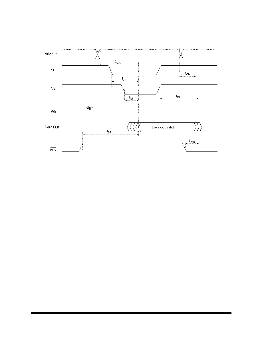
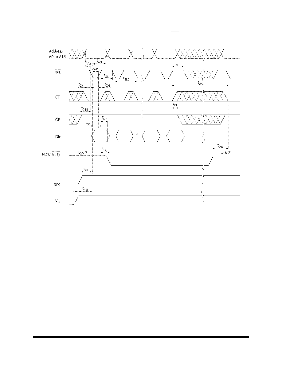
F
IGURE
1. R
EAD
T
IMING
W
AVEFORM

M
e
m
o
r
y
8
All data sheets are subject to change without notice
©2002 Maxwell Technologies
All rights reserved.
3.3V 1 Megabit (128K x 8-Bit) EEPROM
28LV011
05.28.02 Rev 2
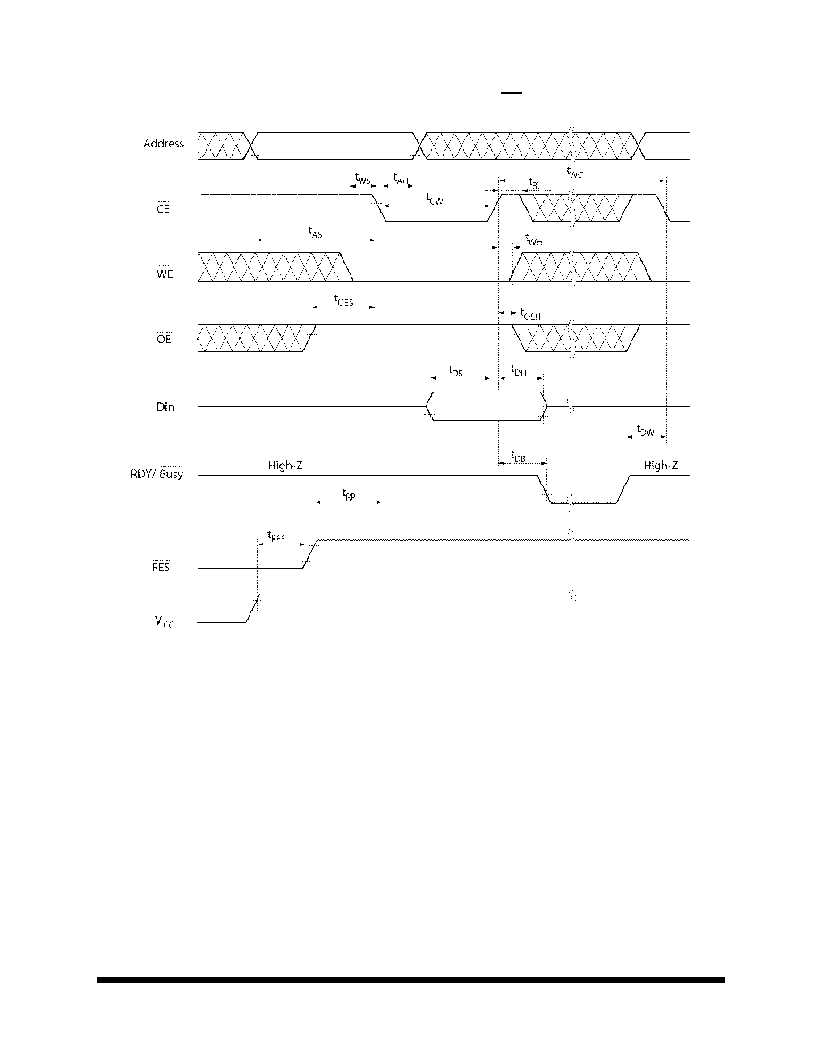
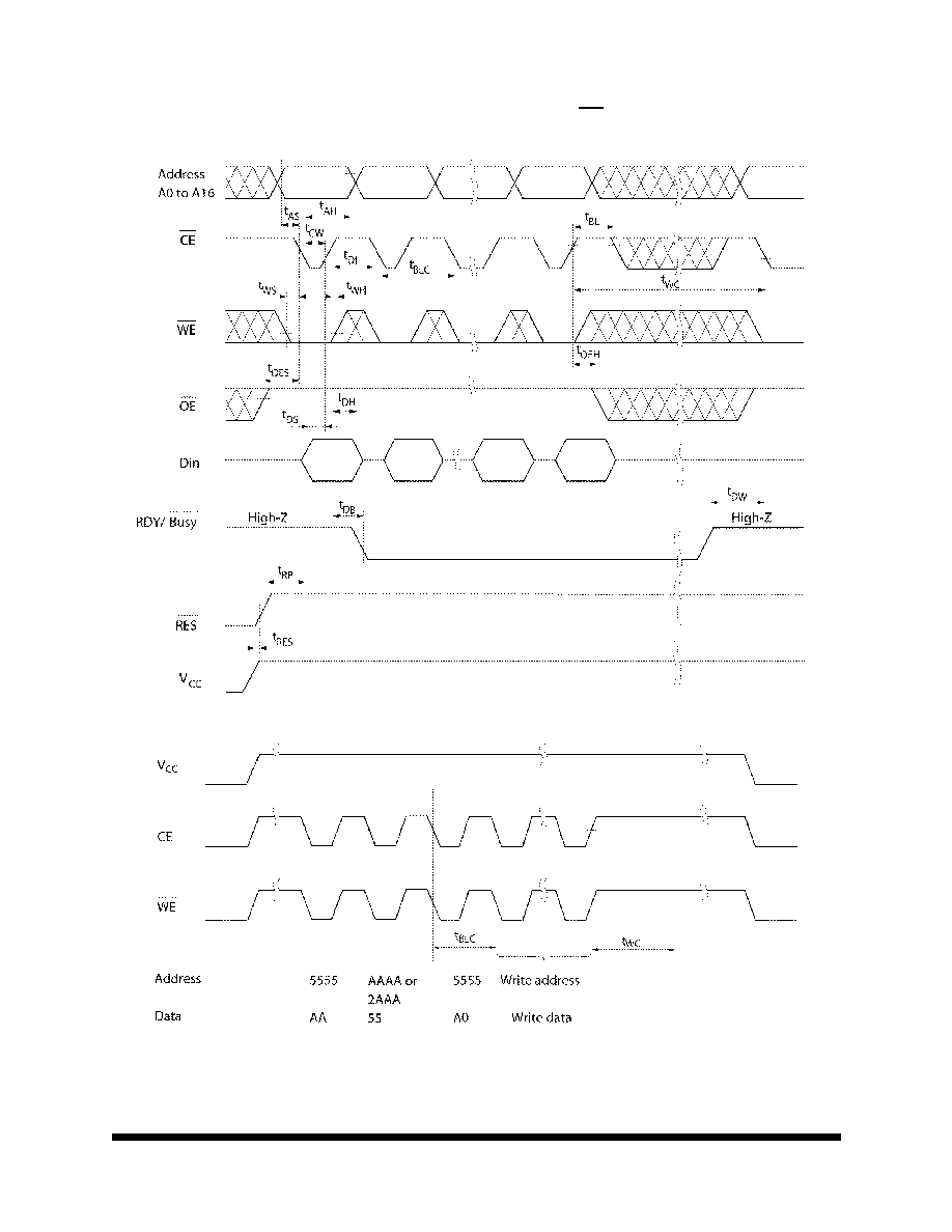
F
IGURE
2. B
YTE
W
RITE
T
IMING
W
AVEFORM
(1) (WE C
ONTROLLED
)
M
e
m
o
r
y
9
All data sheets are subject to change without notice
©2002 Maxwell Technologies
All rights reserved.
3.3V 1 Megabit (128K x 8-Bit) EEPROM
28LV011
05.28.02 Rev 2
F
IGURE
3. B
YTE
W
RITE
T
IMING
W
AVEFORM
(2) (CE C
ONTROLLED
)
M
e
m
o
r
y
10
All data sheets are subject to change without notice
©2002 Maxwell Technologies
All rights reserved.
3.3V 1 Megabit (128K x 8-Bit) EEPROM
28LV011
05.28.02 Rev 2
F
IGURE
4. P
AGE
W
RITE
T
IMING
W
AVEFORM
(1) (WE C
ONTROLLED
)
M
e
m
o
r
y
11
All data sheets are subject to change without notice
©2002 Maxwell Technologies
All rights reserved.
3.3V 1 Megabit (128K x 8-Bit) EEPROM
28LV011
05.28.02 Rev 2
F
IGURE
5. P
AGE
W
RITE
T
IMING
W
AVEFORM
(2) (CE C
ONTROLLED
)
F
IGURE
6. S
OFTWARE
D
ATA
P
ROTECTION
T
IMING
W
AVEFORM
(1) (
IN
PROTECTION
MODE
)
M
e
m
o
r
y
12
All data sheets are subject to change without notice
©2002 Maxwell Technologies
All rights reserved.
3.3V 1 Megabit (128K x 8-Bit) EEPROM
28LV011
05.28.02 Rev 2
F
IGURE
7. S
OFTWARE
D
ATA
P
ROTECTION
T
IMING
W
AVEFORM
(2) (
IN
NON
-
PROTECTION
MODE
)
F
IGURE
8. D
ATA
P
OLLING
T
IMING
W
AVEFORM

M
e
m
o
r
y
13
All data sheets are subject to change without notice
©2002 Maxwell Technologies
All rights reserved.
3.3V 1 Megabit (128K x 8-Bit) EEPROM
28LV011
05.28.02 Rev 2
F
IGURE
9. T
OGGLE
B
IT
W
AVEFORM
F
IGURE
10. SEU S
ATURATED
C
ROSS
S
ECTION
V
ALUES
IN
R
EAD
M
ODE
28LV010 Read Mode Cross-section
1.00E-07
1.00E-06
1.00E-05
1.00E-04
1.00E-03
1.00E-02
0
10
20
30
40
50
60
70
80
90
LET [Mev-cm^2/mg]
C
r
o
ss-sectio
n
[cm
^
2
]
lv1
lv2
lv5
lv6

M
e
m
o
r
y
14
All data sheets are subject to change without notice
©2002 Maxwell Technologies
All rights reserved.
3.3V 1 Megabit (128K x 8-Bit) EEPROM
28LV011
05.28.02 Rev 2
F
IGURE
11. SEU S
ATURATED
C
ROSS
S
ECTION
V
ALUES
IN
W
RITE
M
ODE
EEPROM A
PPLICATION
N
OTES
This application note describes the programming procedures for the EEPROM modules and with details of various
techniques to preserve data protection.
Automatic Page Write
Page-mode write feature allows 1 to 128 bytes of data to be written into the EEPROM in a single write cycle, and
allows the undefined data within 128 bytes to be written corresponding to the undefined address (A0 to A6). Loading
the first byte of data, the data load window opens 30 µ s for the second byte. In the same manner each additional byte
of data can be loaded within 30 µ s. In case CE and WE are kept high for 100s after data input, EEPROM enters erase
and write mode automatically and only the input data are written into the EEPROM.
WE CE Pin Operation
During a write cycle, addresses are latched by the falling edge of WE or CE, and data is latched by the rising edge of
WE or CE.
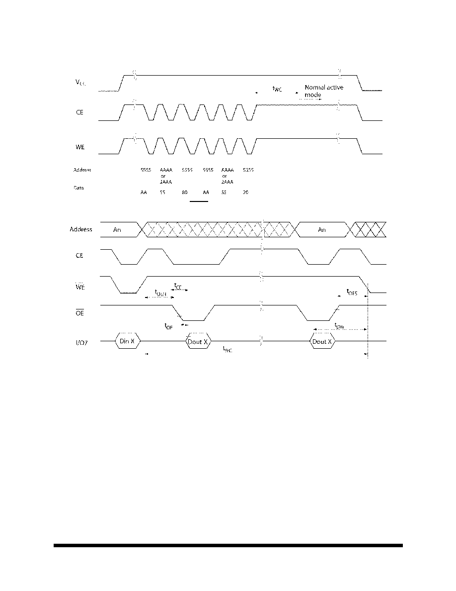
Data Polling
Data Polling function allows the status of the EEPROM to be determined. If EEPROM is set to read mode during a
write cycle, an inversion of the last byte of data to be loaded outputs from I/O 7 to indicate that the EEPROM is per-
forming a write operation.
28LV010 WRITE MODE AVERAGE CROS S -S ECTION
1.00E-06
1.00E-05
1.00E-04
1.00E-03
1.00E-02
1.00E-01
0
10
20
30
40
50
60
70
80
90
LET [Me V-cm^2/mg]
CRO
S
S
-
S
E
CTIO
N [
c
m
^
2
]
SL1
SL2
SL3
N4
N5
M
e
m
o
r
y
15
All data sheets are subject to change without notice
©2002 Maxwell Technologies
All rights reserved.
3.3V 1 Megabit (128K x 8-Bit) EEPROM
28LV011
05.28.02 Rev 2
RDY/Busy Signal
RDY/Busy signal also allows a comparison operation to determine the status of the EEPROM. The RDY/Busy signal
has high impedance except in write cycle and is lowered to V
OL
after the first write signal. At the-end of a write cycle,
the RDY/Busy signal changes state to high impedance.
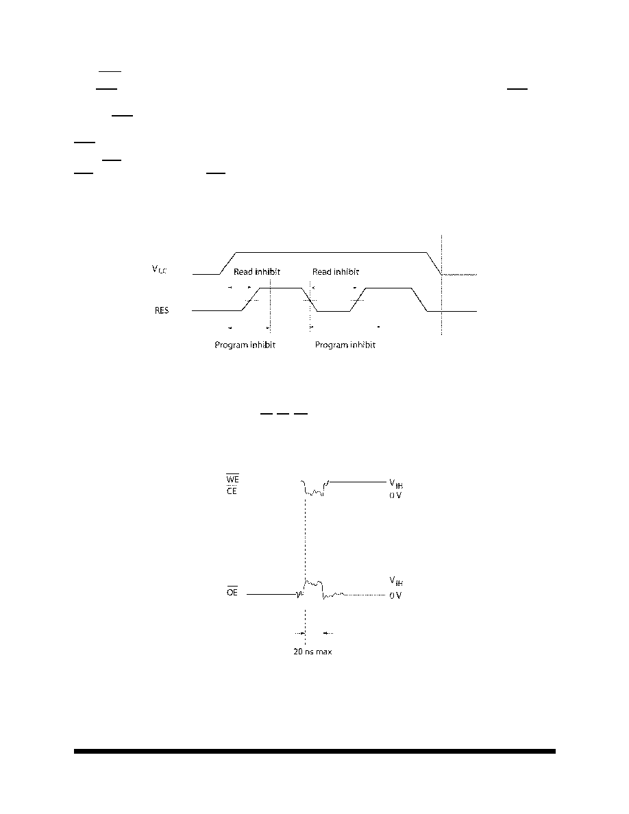
RES Signal
When RES is LOW, the EEPROM cannot be read and programmed. Therefore, data can be protected by keeping
RES low when V
CC
is switched. RES should be high during read and programming because it doesn't provide a latch
function.
Data Protection
To protect the data during operation and power on/off, the EEPROM has the internal functions described below.
1. Data Protection against Noise of Control Pins (CE, OE, WE) during Operation.
During readout or standby, noise on the control pins may act as a trigger and turn the EEPROM to programming mode by mis-
take. To prevent this phenomenon, the EEPROM has a noise cancellation function that cuts noise if its width is 20 ns or less in
programming mode. Be careful not to allow noise of a width of more than 20 ns on the control pins.
2. Data Protection at V
CC
on/off

M
e
m
o
r
y
16
All data sheets are subject to change without notice
©2002 Maxwell Technologies
All rights reserved.
3.3V 1 Megabit (128K x 8-Bit) EEPROM
28LV011
05.28.02 Rev 2
When V
CC
is turned on or off, noise on the control pins generated by external circuits, such as CPUs, may turn the EEPROM to
programming mode by mistake. To prevent this unintentional programming, the EEPROM must be kept in unprogrammable
state during V
CC
on/off by using a CPU reset signal to RES pin.
RES should be kept at V
SS
level when V
CC
is turned on or off. The EEPROM breaks off programming operation when RES
become low, programming operation doesn't finish correctly in case that RES falls low during programming operation. RES
should be kept high for 10 ms after the last data input.
3. Software Data Protection
The software data protection function is to prevent unintentional programming caused by noise generated by external circuits.
In software data protection mode, 3 bytes of data must be input before write data as follows. These bytes can switch the non-
protection mode to the protection mode.
Software data protection mode can be canceled by inputting the following 6 bytes. Then, the EEPROM turns to the non-protec-
tion mode and can write data normally. However, when the data is input in the canceling cycle, the data cannot be written.
M
e
m
o
r
y
17
All data sheets are subject to change without notice
©2002 Maxwell Technologies
All rights reserved.
3.3V 1 Megabit (128K x 8-Bit) EEPROM
28LV011
05.28.02 Rev 2
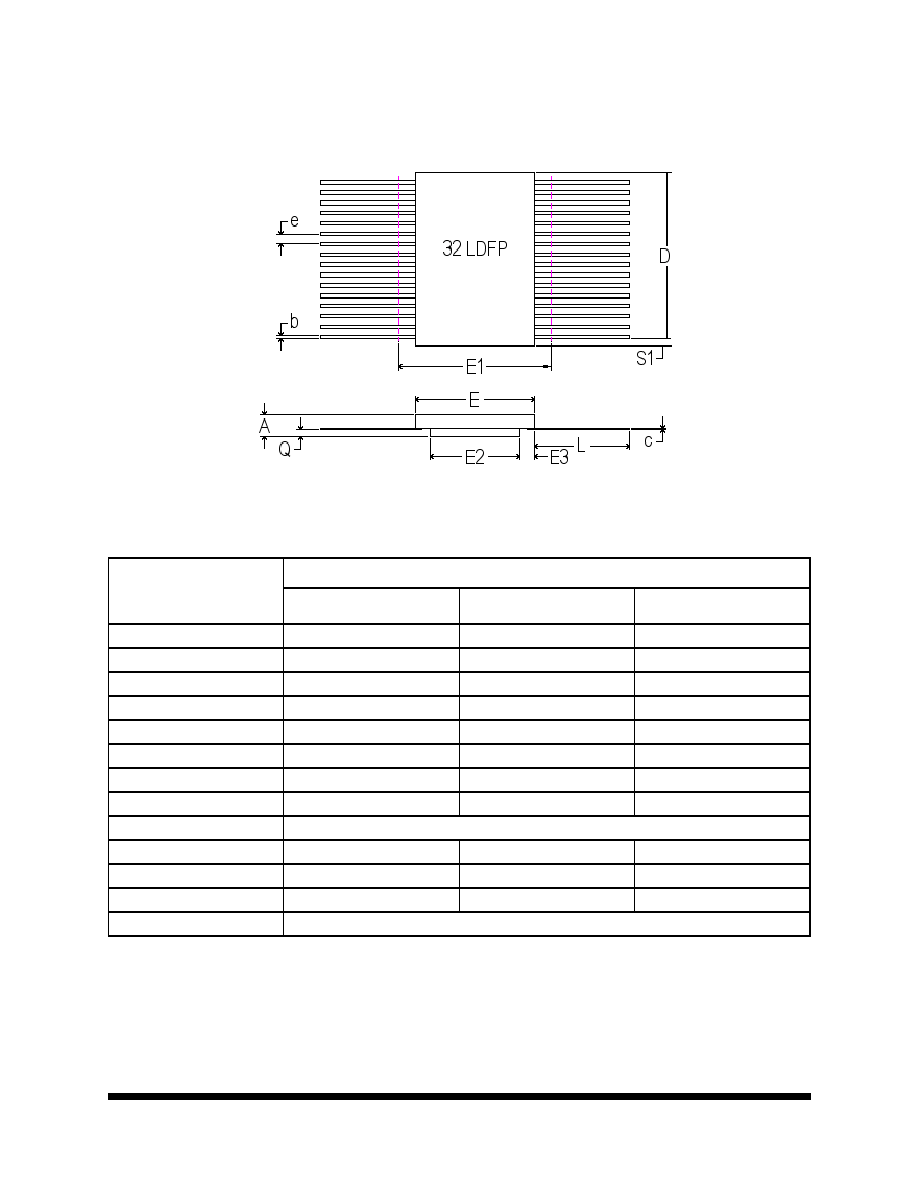
F32-01
Note: All dimensions in inches
32-P
IN
R
AD
-P
AK
Æ F
LAT
P
ACKAGE
S
YMBOL
D
IMENSION
M
IN
N
OM
M
AX
A
0.117
0.130
0.143
b
0.015
0.017
0.022
c
0.003
0.005
0.009
D
--
0.820
0.830
E
0.404
0.410
0.416
E1
--
--
0.440
E2
0.234
0.240
--
E3
0.030
0.085
--
e
0.050BSC
L
0.350
0.370
0.390
Q
0.020
0.035
0.045
S1
0.005
0.027
--
N
32

M
e
m
o
r
y
18
All data sheets are subject to change without notice
©2002 Maxwell Technologies
All rights reserved.
3.3V 1 Megabit (128K x 8-Bit) EEPROM
28LV011
05.28.02 Rev 2
Important Notice:
These data sheets are created using the chip manufacturers published specifications. Maxwell Technologies verifies
functionality by testing key parameters either by 100% testing, sample testing or characterization.
The specifications presented within these data sheets represent the latest and most accurate information available to
date. However, these specifications are subject to change without notice and Maxwell Technologies assumes no
responsibility for the use of this information.
Maxwell Technologies' products are not authorized for use as critical components in life support devices or systems
without express written approval from Maxwell Technologies.
Any claim against Maxwell Technologies must be made within 90 days from the date of shipment from Maxwell Tech-
nologies. Maxwell Technologies' liability shall be limited to replacement of defective parts.
M
e
m
o
r
y
19
All data sheets are subject to change without notice
©2002 Maxwell Technologies
All rights reserved.
3.3V 1 Megabit (128K x 8-Bit) EEPROM
28LV011
05.28.02 Rev 2
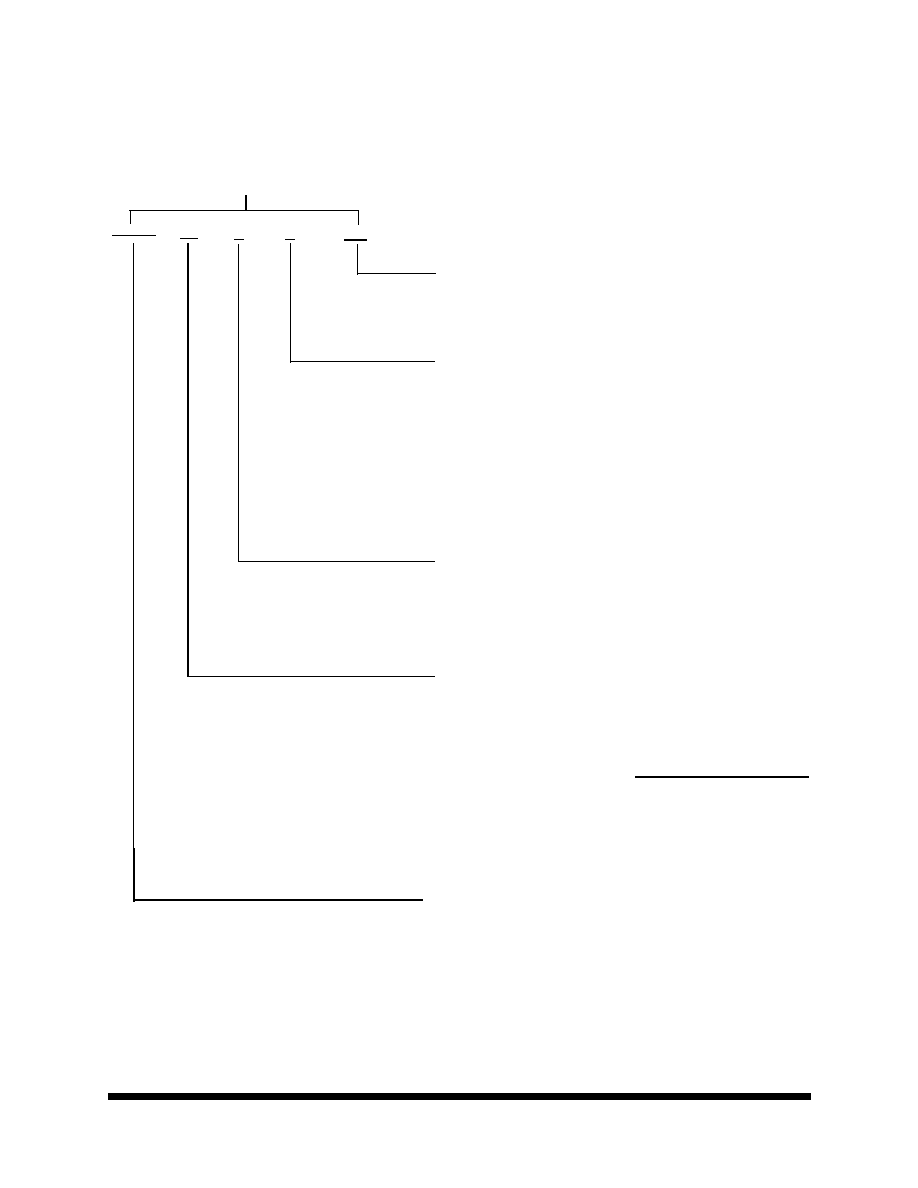
Product Ordering Options
Model Number
Feature
Option Details
28LV011
XX
X
X
-XX
Access Time
Screening Flow
Package
Radiation Feature
Base Product
Nomenclature
20 = 200 ns
25 = 250 ns
Monolithic
S = Maxwell Class S
B = Maxwell Class B
I = Industrial (testing @ -55∞C,
+25∞C, +125∞C)
E = Engineering (testing @ +25∞C)
F = Flat Pack
RP = R
AD
-P
AK
Æ package
RT1
1
= Guaranteed to 10 krad at
die level
RT2
1
= Guaranteed to 25 krad at
die level
RT4
1
= Guaranteed to 40 krad at
die level
1. No Radiation
Guarantee for
Class E & I
3.3V 1 Megabit (128K x 8-Bit)
EEPROM