 | –≠–ª–µ–∫—Ç—Ä–æ–Ω–Ω—ã–π –∫–æ–º–ø–æ–Ω–µ–Ω—Ç: 306RP | –°–∫–∞—á–∞—Ç—å:  PDF PDF  ZIP ZIP |
1
Memory
All data sheets are subject to change without notice
(858) 503-3300 - Fax: (858) 503-3301 - www.maxwell.com
16-Channel CMOS
306
©2001 Maxwell Technologies
All rights reserved.
Analog Multiplexer
08.15.02 Rev 5
F
EATURES
:
∑ R
AD
-P
AKÆ
technology radiation-hardened against natural
space radiation
∑ Total dose hardness:
- > 50 Krad (Si), depending upon space mission
∑ Excellent Single Event Effects:
- SEL
TH
: > 110 MeV/mg/cm
2
- SEU
TH
: > 110 MeV/mg/cm
2
∑ Package: 28-pin R
AD
-P
AKÆ
flat pack
∑ Guaranteed on-resistance matching between channels:
< 5
max
∑ Low on-resistance < 100
max
∑ Guaranteed flat on-resistance over specified signal range:
7
max
∑ Guaranteed Charge Injection: < 10 pC
∑ I
NO(OFF)
Leakage < 2.5 nA at +85
∞
C
∑ I
COM(OFF)
Leakage < 20 nA at +85
∞
C
∑ ESD Protection > 2000V
∑ Single-supply operation (+4.5V to +30V)
∑ Bipolar-supply operation (±4.5V to ±20V)
∑ Low power consumption, < 1.25 mW
∑ Rail-to-rail signal handling
∑ TTL/CMOS-logic compatible
D
ESCRIPTION
:
Maxwell Technologies' 306 high-performance, high-precision,
monolithic, CMOS analog multiplexer features a greater than
50 krad (Si) total dose tolerance, depending upon space mis-
sion. The patented radiation-hardened R
AD
-P
AKÆ
technology
incorporates radiation shielding in the microcircuit package.
Using Maxwell's radiation hardened R
AD
-P
AK
packaging tech-
nology, this single-ended 1-of-16 device offers very low (less
than 100
) on-resistance which is matched to within 5
between channels and remains flat over the specified analog
signal range. The 306 also offers low leakage over tempera-
ture and fast switching speeds. The 306 operates with a single
+4.5V to +30V supply, or bipolar ±4.5V to ± 20V supplies,
while retaining TTL/CMOS- logic input compatibility and fast
switching.
Maxwell Technologies' patented Rad-Pak packaging technol-
ogy incorporates radiation shielding in the microcircuit pack-
age. It eliminates the need for box shielding while providing
the required radiation shielding for a lifetime in orbit or a space
mission.In a GEO orbit, Rad-Pak provides greater than 50
krad (Si) total radiation dose tolerance, dependent upon space
mission. This product is available with packaging and screen-
ing up to Class S.
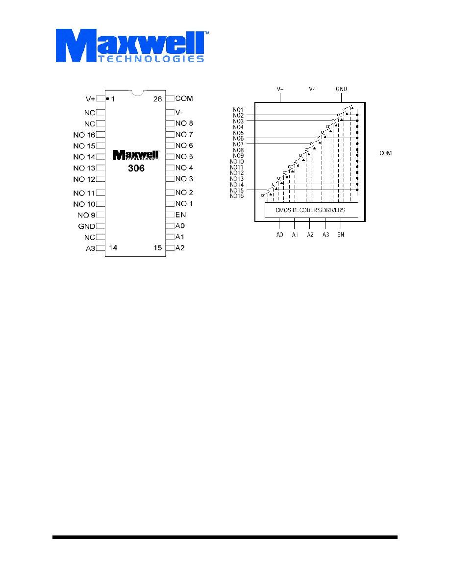
Logic Diagram

Memory
2
All data sheets are subject to change without notice
©2002 Maxwell Technologies
All rights reserved.
16-Channel CMOS Analog Multiplexer
306
08.15.02 Rev 5
T
ABLE
1. P
INOUT
D
ESCRIPTION
P
IN
S
YMBOL
D
ESCRIPTION
1
V+
Positive Supply Voltage Input
2, 3, 13
NC
No Internal Connections
4-11
NO16-NO9 Analog Inputs-bidirectional
12
GND
Ground
14-17
A3-A0
Address Inputs
18
EN
Enable Inputs
19-26
NO1-NO8
Analog Inputs-bidirectional
27
V-
Negative Supply Voltage Input
28
COM
Output-bidirectional
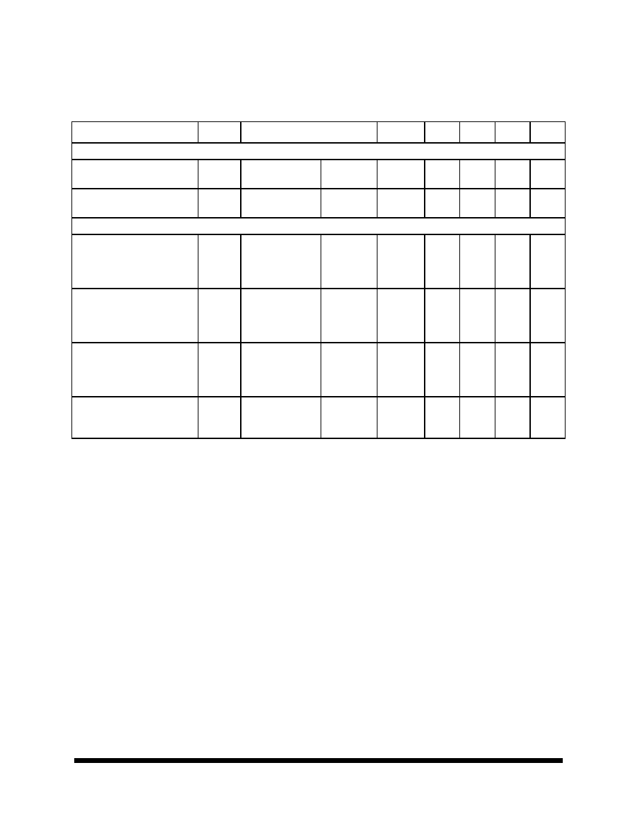
T
ABLE
2. 306 A
BSOLUTE
M
AXIMUM
R
ATINGS
Parameter
Symbol
Min
Max
Units
Voltage Referenced to V-
V+
GND
V
CC
-0.3
-0.3
44
25
V
Digital Inputs, NO, COM
1
1. Signals on NO, COM, A0, A1, A2, A3, or EN exceeding V+ or V- are clamped by internal diodes. Limit forward current to maxi-
mum current ratings.
V- -2
V+ +2
V
Continuous Current any terminal)
2
2. Or 30mA (whichever occurs first)
30
mA
Peak Current, NO or COM (pulsed at 1ms, 10% duty cycle max)
100
mA
Thermal Impedance
JC
--
3.62
∞C/W
Operating Temperature Range:
T
A
-55
+125
∞C
Storage Temperature Range:
T
S
-65
+150
∞C
T
ABLE
3. D
ELTA
L
IMITS
P
ARAMETER
V
ARIATION
I+
±10% of specified value in table 5
I-
±10% of specified value in table 5
Memory
3
All data sheets are subject to change without notice
©2002 Maxwell Technologies
All rights reserved.
16-Channel CMOS Analog Multiplexer
306
08.15.02 Rev 5
T
ABLE
4. 306 E
LECTRICAL
C
HARACTERISTICS
-- S
INGLE
S
UPPLY
(V+ = +12V, V- = 0V, GND = 0V, V
AH
= +2.4V, V
AL
= +0.8V, T
A
= -55
TO
+125∞C,
UNLESS
OTHERWISE
SPECIFIED
.)
P
ARAMETER
S
YMBOL
T
EST
C
ONDITIONS
S
UBGROUPS
M
IN1
T
YP1
1. The Algebraic convention where the most negative value is a minimum and the most positive value a maximum is used in this
data sheet.
M
AX1
U
NITS
SWITCH
Analog Signal Range
2
2. Guaranteed by design.
V
NO
V
COM
1, 2, 3
0
--
12
V
On-Resistance
R
ON
I
NO
= -1.0mA
V
COM
= 3V or 10V
T
A
= +25∞C
1
--
120
175
DYNAMIC
2
Transition Time
t
TRANS
V
NO1
= 8V
V
NO8
= 0V
V
IN
= 2.4V
Figure 9
T
A
= +25∞C
9
--
130
450
nA
Enable Turn-ON Time
t
ON(EN)
V
INH
= 2.4V
V
INL
= 0V
V
NO1
= 5V
Figure 11
T
A
= +25∞C
9
--
--
600
ns
Enable Turn-OFF Time
t
OFF(EN)
V
INH
= 2.4V
V
INL
= 0V
V
NO1
= 5V
Figure 11
T
A
= +25∞C
9
--
--
300
ns
Charge Injection
Q
CL = 1.0nF
VNO = 0V
VS = 0
W
T
A
= +25∞C
9
--
--
10
pC
Memory
4
All data sheets are subject to change without notice
©2002 Maxwell Technologies
All rights reserved.
16-Channel CMOS Analog Multiplexer
306
08.15.02 Rev 5
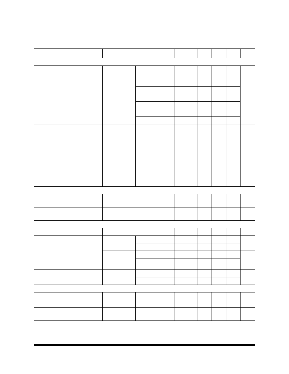
T
ABLE
5. 306 E
LECTRICAL
C
HARACTERISTICS
- D
UAL
S
UPPLIES
(V+ = +15V, V- = -15V, GND = 0V, V
AH
= +2.4V, V
AL
= +0.8V, T
A
= -55
TO
+125∞C,
UNLESS
OTHERWISE
SPECIFIED
.)
P
ARAMETER
S
YMBOL
T
EST
C
ONDITIONS
S
UBGROUPS
M
IN
T
YP
M
AX
U
NITS
SWITCH
Analog Signal Range
1
V
NO
V
COM
1, 2, 3
-15
--
15
V
On-Resistance
R
ON
I
NO
= -1.0 mA
V
COM
= ±10V
T
A
= +25∞C
1
--
60
100
T
A
= -55
TO
+125∞C
2, 3
125
On-Resistance Matching
Between Channels
2, 3
R
ON
I
NO
= -1.0 mA
V
COM
= ±10V
T
A
= +25∞C
1
--
1.5
5
T
A
= -55
TO
+125∞C
2, 3
8
On-Resistance Flatness
2
R
FLAT
I
NO
= -1.0 mA
V
COM
= +5V or 0V
T
A
= +25∞C
1
--
1.8
7
T
A
= -55
TO
+125∞C
2, 3
10
NO-Off Leakage Current
4
I
NO(OFF)
V
COM
= ±10
V
NO
= ±10V
V
EN
= 0V
T
A
= -55
TO
+125∞C
9, 10, 11
-5.0
--
5.0
nA
COM-Off Leakage
Current
4
I
COM(OFF)
V
COM
= ±10
V
NO
= ±10V
V
EN
= 0V
T
A
= -55
TO
+125∞C
9, 10, 11
-40
--
40
nA
COM-On Leakage
Current
4
I
COM(ON)
V
COM
= ±10
V
NO
= ±10V
sequence each
switch on
T
A
= -55
TO
+125∞C
9, 10, 11
-50
--
50
nA
INPUT
Input Current with Input
Voltage High
I
AH
V
A
= 2.4V or 15V
1, 2, 3
-1.0
--
1.0
µA
Input Current with Input
Voltage Low
I
AL
V
EN
= 0V or 2.4V,
V
A
= 0V
1, 2, 3
-1.0
--
1.0
µA
SUPPLY
Power-Supply Range
1, 2, 3
±4.5
--
±20
V
Positive Supply Current
I+
V
EN
= V
A
= 0V or
4.5V
T
A
= +25∞C
1
--
16
30
µA
T
A
= -55
TO
+125∞
2, 3
75
V
EN
= 2.4V,
V
A(ALL)
= 0V or
2.4
T
A
= +25∞C
1
0.075
0.5
mA
T
A
= -55
TO
+125∞C
12, 3
1
Negative Supply Current
I-
V
EN
= 2.4V,
V
A
= 0V or 2.4V
T
A
= +25∞C
1
-1
--
1
µA
T
A
= -55
TO
+125∞C
2, 3
-10
10
DYNAMIC
Transition Time
t
TRANS
Figure 10
T
A
= +25∞C
9
--
110
300
ns
T
A
= -55
TO
+125∞C
10, 11
400
Break-Before-Make Inter-
val
t
OPEN
Figure 12
T
A
= +25∞C
9
10
40
ns

Memory
5
All data sheets are subject to change without notice
©2002 Maxwell Technologies
All rights reserved.
16-Channel CMOS Analog Multiplexer
306
08.15.02 Rev 5
Enable Turn-On Time
t
ON(EN)
Figure 11
T
A
= +25∞C
9
--
130
200
ns
T
A
= -55
TO
+125∞C
10, 11
400
Enable Turn-Off Time
t
OFF(EN)
Figure 11
T
A
= +25∞C
9
--
55
150
ns
T
A
= -55
TO
+125∞C
10, 11
300
Charge Injection
1
Q
C
L
= 1.0 nF,
V
NO
= 0V,
R
S
= 0
,
Figure 13
T
A
= +25∞C
9
--
2
10
pC
Off Isolation
5
V
ISO
V
EN
= 0V,
R
L
= 1 k
,
f = 100 kHz
,
Figure 14
T
A
= +25∞C
9
--
-69
--
dB
Crosstalk Between Chan-
nels
V
CT
V
EN
= 2.4V,
f = 100 kHz
,
V
GEN
= 1V p-p,
R
L
= 1 k
,
Figure 15
T
A
= +25∞C
9
--
-92
--
dB
Logic Input Capacitance
C
IN
f = 1 MHz
T
A
= +25∞C
9
--
8
--
pF
NO-Off Capacitance
C
NO(OFF)
f = 1 MHz
V
EN
= V
NO
= 0V
Figure 16
T
A
= +25∞C
9
--
8
--
pF
COM-Off Capacitance
C
COM(OFF)
f = 1 MHz
V
EN
= 2.4V
Figure 16
T
A
= +25∞C
9
--
130
--
pF
COM-On Capacitance
C
COM(ON)
f = 1 MHz
V
EN
= 0.8V
Figure 16
T
A
= +25∞C
9
--
140
--
pF
1. Guaranteed by design.
2. Characterized and not 100% tested.
3.
RON = RON
(MAX)
- RON
(MIN)
. On-resistance match between channels and flatness are guaranteed only with specified volt-
ages. Flatness is defined as the difference between the maximum and minimum value of on-resistance as measured at the
extremes of the specified analog signal range.
4. Leakage parameters are 100% tested at the maximum rated hot temperature and guaranteed by correlation at +25∞C.
5. Off isolation = 20log V
COM
/V
NO
, where V
COM
= output and V
NO
= input to off switch.
P
ARAMETER
S
YMBOL
T
EST
C
ONDITIONS
S
UBGROUPS
M
IN
T
YP
M
AX
U
NITS