1
M
e
m
o
r
y
All data sheets are subject to change without notice
(858) 503-3300 - Fax: (858) 503-3301 - www.maxwell.com
4 Megabit (512K x 8-Bit)
33LV408
©2004 Maxwell Technologies
All rights reserved.
CMOS SRAM
04.02.04 REV 2
F
EATURES
:
∑ R
AD
-P
AK
Æ
Technology radiation-hardened against natural
space radiation
∑ 524,288 x 8 bit organization
∑
Total dose hardness:
- > 100 krad (Si), depending upon space mission
∑ Excellent Single Event Effect
∑
- SEL
TH
: > 101 MeV/mg/cm
2
∑
- SEU
TH
: = 3 MeV/mg/cm
2
- SEU saturated cross section: 6E-9 cm
2
/bit
∑ Package:
- 32-Pin R
AD
-P
AK
Æ flat pack
∑ Fast access time:
- 20, 25, 30 ns maximum times available
∑ Single 3.3V + 10% power supply
∑ Fully static operation
- No clock or refresh required
∑ Three state outputs
∑ TTL compatible inputs and outputs
∑ Low power:
- Standby: 60 mA (TTL); 10 mA (CMOS)
- Operation: 150 mA (20 ns); 140 mA (25 ns);
130 mA (30 ns)
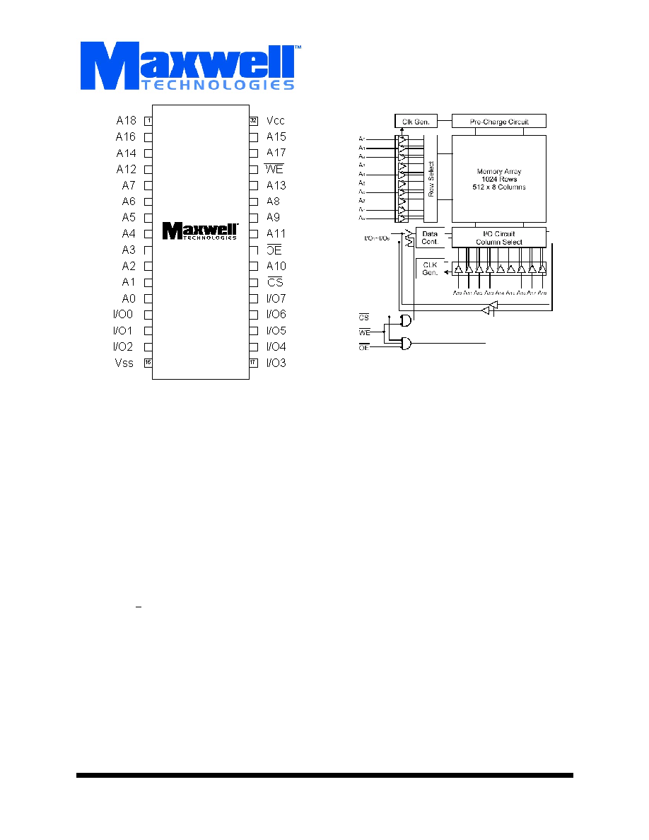
D
ESCRIPTION
:
Maxwell Technologies' 33LV408 high-density 4 Megabit
SRAM microcircuit features a greater than 100 krad (Si) total
dose tolerance, depending upon space mission. Using Max-
well's radiation-hardened R
AD
-P
AK
Æ packaging technology, the
33LV408 realizes a high density, high performance, and low
power consumption. Its fully static design eliminates the need
for external clocks, while the CMOS circuitry reduces power
consumption and provides higher reliability. The 33LV408 is
equipped with eight common input/output lines, chip select
and output enable, allowing for greater system flexibility and
eliminating bus contention. The 33LV408 features the same
advanced 512K x 8-bit SRAM, high-speed, and low-power
demand as the commercial counterpart.
Maxwell Technologies' patented R
AD
-P
AK
Æ packaging technol-
ogy incorporates radiation shielding in the microcircuit pack-
age. It eliminates the need for box shielding while providing
the required radiation shielding for a lifetime in orbit or space
mission. In a GEO orbit, R
AD
-P
AK
Æ provides greater than 100
krad (Si) radiation dose tolerance. This product is available
with screening up to Class S.
Logic Diagram
33LV408
M
e
m
o
r
y
2
All data sheets are subject to change without notice
©2004 Maxwell Technologies
All rights reserved.
4 Megabit (512K x 8-Bit) CMOS SRAM
33LV408
04.02.04 REV 2
T
ABLE
1. P
INOUT
D
ESCRIPTION
P
IN
S
YMBOL
D
ESCRIPTION
12-5, 27, 26, 23, 25, 4,
28, 3, 31, 2, 30, 1
A0-A18
Address Inputs
29
WE
Write Enable
22
CS
Chip Select
24
OE
Output Enable
13-15, 17-21
I/O 1-I/O 8
Data Inputs/Outputs
32
V
CC
Power
16
V
SS
Ground
T
ABLE
2. 33LV408 A
BSOLUTE
M
AXIMUM
R
ATINGS
P
ARAMETER
S
YMBOL
M
IN
M
AX
U
NIT
Voltage on V
CC
supply relative to V
SS
V
CC
-0.5
7.0
V
Voltage on any pin relative to V
SS
V
IN
, V
OUT
-0.5
V
CC
+0.5
V
Power Dissipation
P
D
--
1.0
W
Storage Temperature
T
S
-65
+150
∞
C
Operating Temperature
T
A
-55
+125
∞
C
T
ABLE
3. D
ELTA
L
IMITS
P
ARAMETER
V
ARIATION
I
CC
±10% of stated vaule in Table 6
I
SB
±10% of stated vaule in Table 6
I
SB1
±10% of stated vaule in Table 6
M
e
m
o
r
y
3
All data sheets are subject to change without notice
©2004 Maxwell Technologies
All rights reserved.
4 Megabit (512K x 8-Bit) CMOS SRAM
33LV408
04.02.04 REV 2
T
ABLE
4. 33LV408 R
ECOMMENDED
O
PERATING
C
ONDITIONS
(V
CC
= 3.3 + 10%, T
A
= -55
TO
+125
∞
C,
UNLESS
OTHERWISE
NOTED
)
P
ARAMETER
S
YMBOL
M
IN
M
AX
U
NIT
Supply Voltage
V
CC
3.0
3.6
V
Ground
V
SS
0
0
V
Input High Voltage
1
1. V
IH
(max) = V
CC
+2.0V ac (pulse width < 10 ns) for I < 20 mA
V
IH
2.2
V
CC
+0.3
V
Input Low Voltage
2
2. V
IL
(min) = -2.0V ac(pulse width < 10 ns) for I < 20 mA
V
IL
-0.3
0.8
V
Thermal Impedance
JC
--
1.21
∞C/W
Weight
12
Grams
T
ABLE
5. 33LV408 C
APACITANCE
(f = 1.0 MH
Z
, V
CC
= 3.3 V, T
A
= 25
∞
C)
P
ARAMETER
S
YMBOL
T
EST
C
ONDITIONS
M
AX
U
NITS
Input Capacitance
1
CS1 - CS4,
OE, WE
I/O0-7, I/O8-15, I/O16-23, I/O24-31
1. Guaranteed by design.
C
IN
V
IN
= 0 V
7
28
7
pF
Input / Output Capacitance
1
C
OUT
V
I/O
= 0 V
8
pF
T
ABLE
6. 33LV408 DC E
LECTRICAL
C
HARACTERISTICS
(V
CC
= 3.3V + 10%, T
A
= -55
TO
+125
∞
C,
UNLESS
OTHERWISE
SPECIFIED
)
P
ARAMETER
S
YMBOL
C
ONDITION
S
UBGROUPS
M
IN
M
AX
U
NIT
Input Leakage Current
I
LI
V
IN
= V
SS
to V
CC
1, 2, 3
-2
2
µ A
Output Leakage Current
I
LO
CS=V
IH
or OE=V
IH
or WE=V
IL
,
V
OUT
=V
SS
to V
CC
1, 2, 3
-2
2
µ A
Output Low Voltage
V
OL
I
OL
= 8mA
1, 2, 3
--
0.4
V
Output High Voltage
V
OH
I
OH
= -4mA
1, 2, 3
2.4
--
V
Operating Current
-20
-25
-30
I
CC
Min cycle, 100% Duty, CS=V
IL
, I
OUT
=0mA,
V
IN
= V
IH
or V
IL
1, 2, 3
--
--
--
150
140
130
mA
Standby Power Supply
Current
I
SB
CS = V
IH
, Min Cycle
1, 2, 3
--
60
mA

M
e
m
o
r
y
4
All data sheets are subject to change without notice
©2004 Maxwell Technologies
All rights reserved.
4 Megabit (512K x 8-Bit) CMOS SRAM
33LV408
04.02.04 REV 2
Standby Power Supply
Current - CMOS
I
SB1
CS > V
CC
- 0.2V; V
IN
> V
CC
- 0.2V
or V
IN
< 0.2V
1, 2, 3
--
10
mA
Input Capacitance
1
C
IN
V
IN
= 0V, f = 1MHz, T
A
= 25 ∞C
1, 2, 3
--
7
pF
Output Capacitance
1
C
I/O
V
I/O
= 0V
1, 2, 3
--
8
pF
1. Guaranteed by design.
T
ABLE
7. 33LV408 AC O
PERATING
C
ONDITIONS
AND
C
HARACTERISTICS
(V
CC
= 3.3 + 10%, T
A
= -55
TO
+125
∞
C,
UNLESS
OTHERWISE
NOTED
)
P
ARAMETER
M
IN
T
YP
M
AX
U
NITS
Input Pulse Level
0.0
--
3.0
V
Output Timing Measurement Reference Level
--
--
1.5
V
Input Rise/Fall Time
--
--
3.0
ns
Input Timing Measurement Reference Level
--
--
1.5
V
T
ABLE
8. 33LV408 AC C
HARACTERISTICS
FOR
R
EAD
C
YCLE
(V
CC
= 3.3V + 10%, T
A
= -55
TO
+125
∞
C,
UNLESS
OTHERWISE
SPECIFIED
)
P
ARAMETER
S
YMBOL
S
UBGROUPS
M
IN
T
YP
M
AX
U
NIT
Read Cycle Time
-20
-25
-30
t
RC
9, 10, 11
20
25
30
--
--
--
--
--
--
ns
Address Access Time
-20
-25
-30
t
AA
9, 10, 11
--
--
--
--
--
--
20
25
30
ns
Chip Select Access Time
-20
-25
-30
t
CO
9, 10, 11
--
--
--
--
--
--
20
25
30
ns
Output Enable to Output Valid
-20
-25
-30
t
OE
9, 10, 11
--
--
--
--
--
--
10
12
14
ns
Chip Enable to Output in Low-Z
-20
-25
-30
t
LZ
9, 10, 11
--
--
--
3
3
3
--
--
--
ns
T
ABLE
6. 33LV408 DC E
LECTRICAL
C
HARACTERISTICS
(V
CC
= 3.3V + 10%, T
A
= -55
TO
+125
∞
C,
UNLESS
OTHERWISE
SPECIFIED
)
P
ARAMETER
S
YMBOL
C
ONDITION
S
UBGROUPS
M
IN
M
AX
U
NIT
M
e
m
o
r
y
5
All data sheets are subject to change without notice
©2004 Maxwell Technologies
All rights reserved.
4 Megabit (512K x 8-Bit) CMOS SRAM
33LV408
04.02.04 REV 2
Output Enable to Output in Low-Z
-20
-25
-30
t
OLZ
9, 10, 11
--
--
--
0
0
0
--
--
--
ns
Chip Deselect to Output in High-Z
-20
-25
-30
t
HZ
9, 10, 11
--
--
--
5
6
8
--
--
--
ns
Output Disable to Output in High-Z
-20
-25
-30
t
OHZ
9, 10, 11
--
--
--
5
6
8
--
--
--
ns
Output Hold from Address Change
-20
-25
-30
t
OH
9, 10, 11
3
5
6
--
--
--
--
--
--
ns
Chip Select to Power Up Time
-20
-25
-30
t
PU
9, 10, 11
--
--
--
0
0
0
--
--
--
ns
Chip Select to Power Down Time
-20
-25
-30
t
PD
9, 10, 11
--
--
--
10
15
20
--
--
--
ns
T
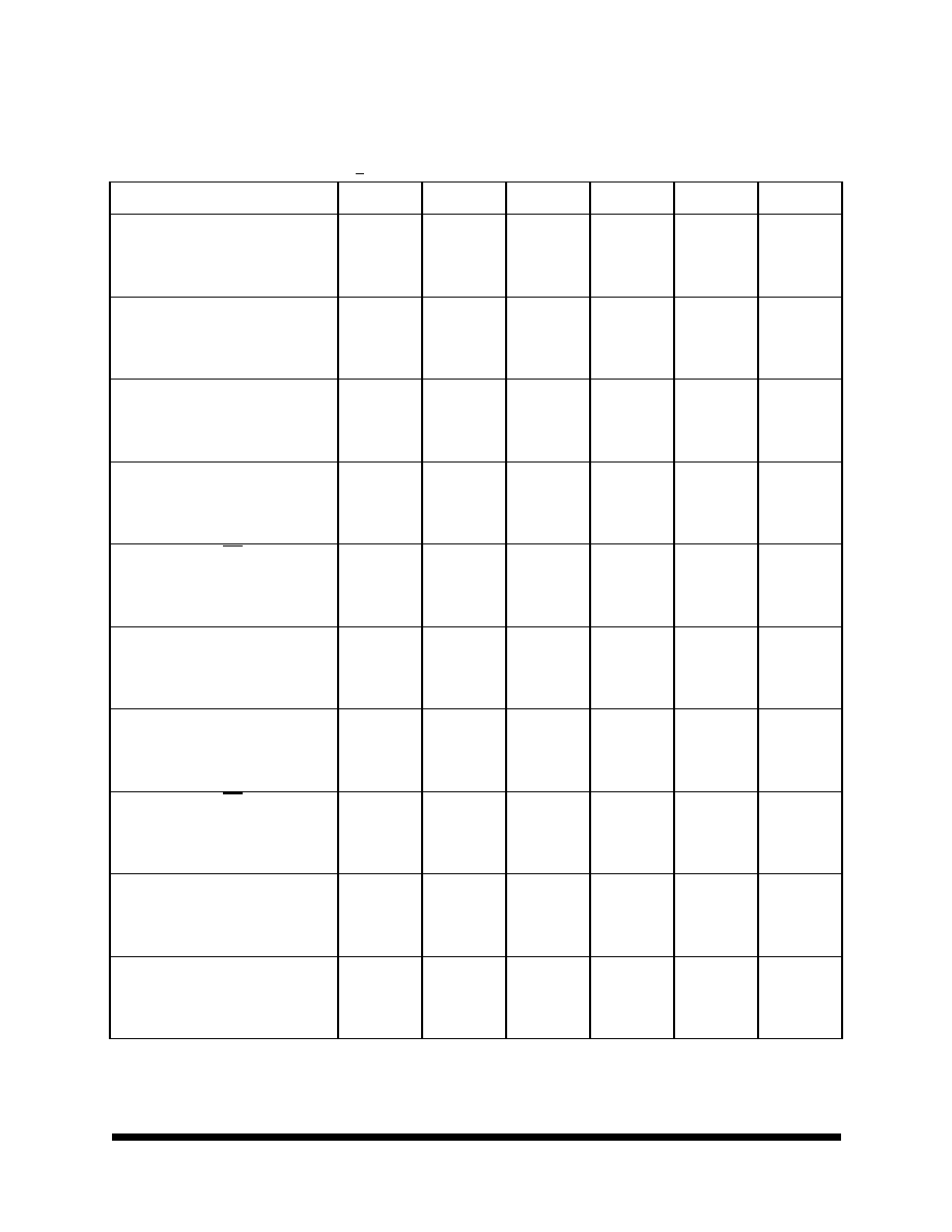
ABLE
9. 33LV408 F
UNCTIONAL
D
ESCRIPTION
CS
WE
OE
M
ODE
I/O P
IN
S
UPPLY
C
URRENT
H
X
1
1. X = don't care.
X
1
Not Select
High-Z
I
SB
, I
SB1
L
H
H
Output Disable
High-Z
I
CC
L
H
L
Read
D
OUT
I
CC
L
L
X
1
Write
D
IN
I
CC
T
ABLE
8. 33LV408 AC C
HARACTERISTICS
FOR
R
EAD
C
YCLE
(V
CC
= 3.3V + 10%, T
A
= -55
TO
+125
∞
C,
UNLESS
OTHERWISE
SPECIFIED
)
P
ARAMETER
S
YMBOL
S
UBGROUPS
M
IN
T
YP
M
AX
U
NIT
M
e
m
o
r
y
6
All data sheets are subject to change without notice
©2004 Maxwell Technologies
All rights reserved.
4 Megabit (512K x 8-Bit) CMOS SRAM
33LV408
04.02.04 REV 2
T
ABLE
10. 33LV408 AC C
HARACTERISTICS
FOR
W
RITE
C
YCLE
(V
CC
= 3.3V + 10%, T
A
= -55
TO
+125
∞
C,
UNLESS
OTHERWISE
SPECIFIED
)
P
ARAMETER
S
YMBOL
S
UBGROUPS
M
IN
T
YP
M
AX
U
NIT
Write Cycle Time
-20
-25
-30
t
WC
9, 10, 11
20
25
30
--
--
--
--
--
--
ns
Chip Select to End of Write
-20
-25
-30
t
CW
9, 10, 11
14
15
17
--
--
--
--
--
--
ns
Address Setup Time
-20
-25
-30
t
AS
9, 10, 11
0
0
0
--
--
--
--
--
--
ns
Address Valid to End of Write
-20
-25
-30
t
AW
9, 10, 11
14
15
17
--
--
--
--
--
--
ns
Write Pulse Width (OE High)
-20
-25
-30
t
WP
9, 10, 11
14
15
17
--
--
--
--
--
--
ns
Write Recovery Time
-20
-25
-30
t
WR
9, 10, 11
0
0
0
--
--
--
--
--
--
ns
Write to Output in High-Z
-20
-25
-30
t
WHZ
9, 10, 11
--
--
--
5
5
6
--
--
--
ns
Write Pulse Width (OE Low)
-20
-25
-30
t
WP1
9, 10, 11
--
--
--
20
25
30
--
--
--
ns
Data to Write Time Overlap
-20
-25
-30
t
DW
9, 10, 11
9
10
11
--
--
--
--
--
--
ns
End Write to Output Low-Z
-20
-25
-30
t
OW
9, 10, 11
--
--
--
6
7
8
--
--
--
ns
M
e
m
o
r
y
7
All data sheets are subject to change without notice
©2004 Maxwell Technologies
All rights reserved.
4 Megabit (512K x 8-Bit) CMOS SRAM
33LV408
04.02.04 REV 2
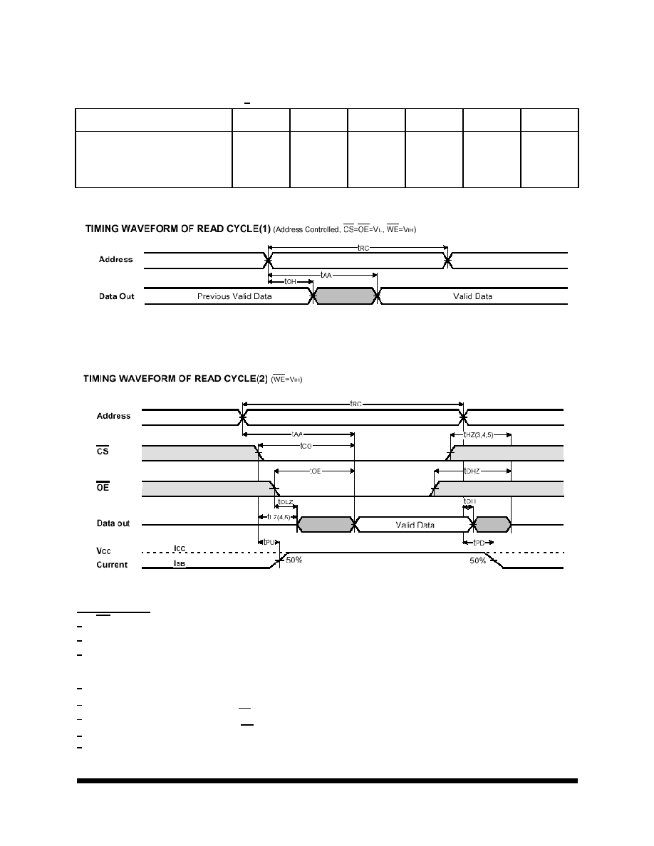
F
IGURE
1: T
IMING
W
AVEFORM
OF
R
EAD
C
YCLE
(1)
F
IGURE
2: T
IMING
W
AVEFORM
OF
R
EAD
C
YCLE
(2)
Read Cycle Notes:
1.
WE is high for read cycle.
2.
All read cycle timing is referenced form the last valid address to the first transition address.
3.
t
HZ
and t
OHZ
are defined as the time at which the outputs achieve the open circuit condition and are not referenced to V
OH
or
V
OL
levels.
4.
At any given temperature and voltage condition, t
HZ(max)
is less than t
LZ(min)
both for a given device and from device to device.
5.
Transition is measured + 200mV from steady state voltage with Load(B). This parameter is sampled and not 100% tested.
6.
Device is continuously selected with CS = V
IL.
7.
Address valid prior to coincident with CS transition low.
8. For common I/O applications, minimization or elimination of bus contention condition is necessary during read and write cycle.
Data Hold from Write Time
-20
-25
-30
t
DH
9, 10, 11
0
0
0
--
--
--
--
--
--
ns
T
ABLE
10. 33LV408 AC C
HARACTERISTICS
FOR
W
RITE
C
YCLE
(V
CC
= 3.3V + 10%, T
A
= -55
TO
+125
∞
C,
UNLESS
OTHERWISE
SPECIFIED
)
P
ARAMETER
S
YMBOL
S
UBGROUPS
M
IN
T
YP
M
AX
U
NIT
M
e
m
o
r
y
8
All data sheets are subject to change without notice
©2004 Maxwell Technologies
All rights reserved.
4 Megabit (512K x 8-Bit) CMOS SRAM
33LV408
04.02.04 REV 2
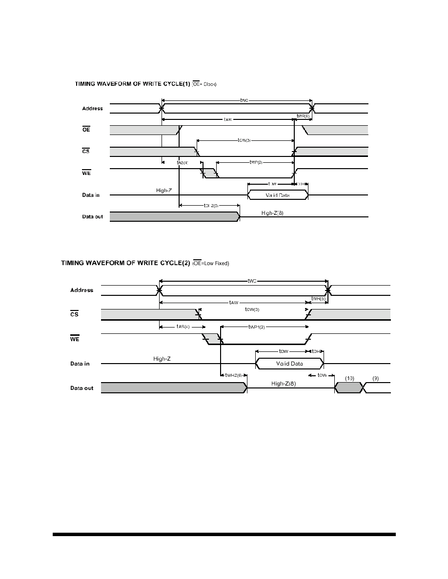
F
IGURE
3: T
IMING
W
AVEFORM
OF
W
RITE
C
YCLE
(1)
F
IGURE
4: T
IMING
W
AVEFORM
OF
W
RITE
C
YCLE
(2)
M
e
m
o
r
y
9
All data sheets are subject to change without notice
©2004 Maxwell Technologies
All rights reserved.
4 Megabit (512K x 8-Bit) CMOS SRAM
33LV408
04.02.04 REV 2
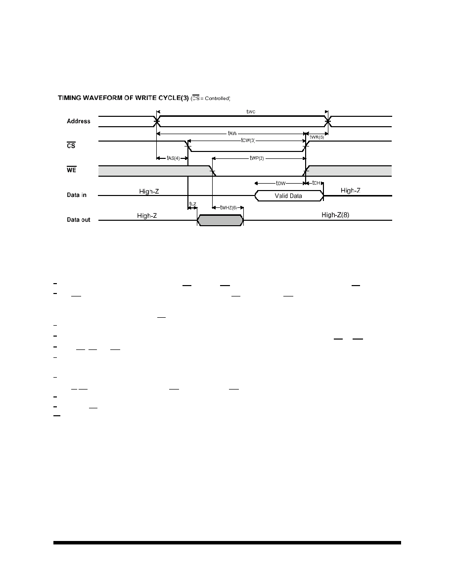
F
IGURE
5: T
IMING
W
AVEFORM
OF
W
RITE
C
YCLE
(3)
W
RITE
C
YCLE
N
OTE
:
1.
All write cycle timing is referenced from the last valid address to the first transition address.
2.
A write occurs during the overlap of a low CS and a low WE. A write begins at the latest transition among CS going low and
WE going low: A write ends at the earliest transition among CS going high and WE going high. t
WP
is measured from begin-
ning of write to the end of write.
3.
t
CW
is measured from the later of CS going low to end of write.
4.
t
AS
is measured from the address valid to the beginning of write.
5.
t
WR
is measured form the end of write to the address change. TWR applied in case a write ends as CS, or WR going high.
6.
If OE, CS and WE are in the Read Mode during this period, the I/O pins are in the output low-Z state. Inputs of opposite
phase of the output must not be applied because bus contention can occur.
7.
For common I/O applications, minimization or elimination of bus contention conditions is necessary during read and write
cycle.
8.
IC CS goes low simultaneously with WE going low or after WE going low, the outputs remain high impedance state.
9.
D
OUT
is the read data of the new address.
10.
When CS is low: I/O pins are in the output state. The input signals in the opposite phase leading to the output should
not be applied.

M
e
m
o
r
y
10
All data sheets are subject to change without notice
©2004 Maxwell Technologies
All rights reserved.
4 Megabit (512K x 8-Bit) CMOS SRAM
33LV408
04.02.04 REV 2
Note: All dimensions in inches
32 P
IN
R
AD
-P
AK
Æ F
LAT
P
ACKAGE
S
YMBOL
D
IMENSION
M
IN
N
OM
M
AX
A
0.122
0.135
0.155
b
0.015
0.017
0.019
c
0.008
0.010
0.012
D
--
0.930
0.940
E
0.635
0.645
0.655
E1
--
--
0.690
E2
0.550
0.565
--
E3
--
0.040
--
e
0.050 BSC
L
0.390
0.400
0.410
Q
0.088
0.098
.108
S1
--
0.082
--
N
32

M
e
m
o
r
y
11
All data sheets are subject to change without notice
©2004 Maxwell Technologies
All rights reserved.
4 Megabit (512K x 8-Bit) CMOS SRAM
33LV408
04.02.04 REV 2
Important Notice:
These data sheets are created using the chip manufacturers published specifications. Maxwell Technologies verifies
functionality by testing key parameters either by 100% testing, sample testing or characterization.
The specifications presented within these data sheets represent the latest and most accurate information available to
date. However, these specifications are subject to change without notice and Maxwell Technologies assumes no
responsibility for the use of this information.
Maxwell Technologies' products are not authorized for use as critical components in life support devices or systems
without express written approval from Maxwell Technologies.
Any claim against Maxwell Technologies must be made within 90 days from the date of shipment from Maxwell Tech-
nologies. Maxwell Technologies' liability shall be limited to replacement of defective parts.
M
e
m
o
r
y
12
All data sheets are subject to change without notice
©2004 Maxwell Technologies
All rights reserved.
4 Megabit (512K x 8-Bit) CMOS SRAM
33LV408
04.02.04 REV 2
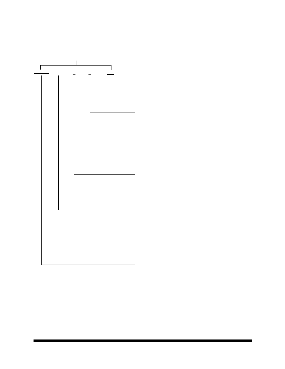
Product Ordering Options
Model Number
Feature
Option Details
33LV408
XX
F
X
-XX
Access Time
Screening Flow
Package
Radiation Feature
Base Product
Nomenclature
20 = 20 ns
25 = 25 ns
30 = 30 ns
Monolithic
S = Maxwell Class S
B = Maxwell Class B
I = Industrial (testing @ -55∞C,
+25∞C, +125∞C)
E = Engineering (testing @ +25∞C)
F = Flat Pack
RP = R
AD
-P
AK
Æ package
4 Megabit CMOS SRAM