1
M
e
m
o
r
y
All data sheets are subject to change without not
ice
(858) 503-3300 Fax: (858) 503-3301 - www.maxwell.com
16-Bit, 20 KHz A/D Converter
©2005 Maxwell Technologies Inc.
All rights reserved.
01.17.05 R
EV
3
5102ALP
F
EATURES
:
∑ Monolithic CMOS A/D converters
- Inherent sampling architecture
- 2-channel input multiplexer
- Flexible serial output port
∑ Conversion time
- 5102A: 40 µ s
∑ Linearity error: ±0.001% FS
- Guaranteed no missing codes
∑ Self-calibration maintains accuracy
- Over time and temperature
∑ Fully latchup protected
D
ESCRIPTION
:
Maxwell Technologies' 5102ALPRP is a 16-bit mono-
lithic CMOS analog-to-digital converter capable of 20
kHz throughput. On-chip self-calibration achieves nonlin-
earity of ±0.001% of FS and guarantees 16-bit no miss-
ing codes over the entire specified temperature range.
Offset and full-scale errors are minimized during the cali-
bration cycle, eliminating the need for external trimming.
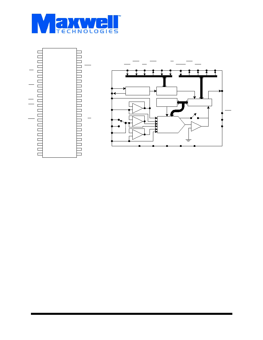
The 5102ALP each consist of a 2-channel input multi-
plexer, DAC, conversion and calibration microcontroller,
clock generator, comparator, and serial communications
port. The inherent sampling architecture of the device
eliminates the need for an external track and hold ampli-
fier.
Maxwell Technologies' patented R
AD
-P
AK
Æ packaging
technology incorporates radiation shielding in the micro-
circuit package. It eliminates the need for box shielding
while improving the TID performance in most space
environments. This product is available with screening
up to Maxwell Technologies self-defined Class K.
Clock
Generator
Control
Calibration
SRAM
Microcontroller
16-Bit charge
Redistribution
DAC
-
+
-
+
-
+
-
+
Comparator
CLKIN
XOUT
REFBUF
VREF
AIN1
AIN2
CH1/2
AGND
VA+
VA-
DGND
VD-
VD+
SCLK
TEST
SCKMOD
OUTMOD
HOLD
SLEEP
RST
STBY
CODE
BP/UP
CRS/FIN
TRK1
TRK2
SSH/SDL
SDATA
1
44
23
22
+VDIG
DGND
-VDIG
RST
CLKIN
XOUT
STBY
DGND
+VDIG
TRK1
TRK2
CRS/FIN
SSH/SDL
HOLD
CH1/2
SCLK
+LPTBIT
NC
-VDIG
-VDIG
DGND
+VDIG
+VAN
AGND
-VANLOG
-LPTV
+LPTV
SDATA
CODE
BP/UP
OUTMOD
AIN1
VREF
REFBUF
AGND
-VANLOG
AIN2
+VANLOG
LPTSTATUS
SCKMOD
SLEEP
-VANLOG
AGND
+VANLOG

M
e
m
o
r
y
2
01.17.05 R
EV
3
All data sheets are subject to change without notice
©2005 Maxwell Technologies Inc.
All rights reserved.
5102ALP
16-Bit, 20 KHz A/D Converter
T
ABLE
1. 5102ALP A
BSOLUTE
M
AXIMUM
R
ATINGS
(AGND, DGND = 0V,
ALL
VOLTAGES
WITH
RESPECT
TO
GROUND
)
P
ARAMETER
S
YMBOL
M
IN
M
AX
U
NIT
DC Power Supplies:
1
Positive Digital
Negative Digital
Positive Analog
Negative Analog
1. In addition, VD+ must not be greater than (VA+) 0.3V.
VD+
VD-
VA+
VA-
-0.3
0.3
-0.3
0.3
6.0
-6.0
6.0
-6.0
V
Input Current, Any Pin Except Supplies
2
2. Transient currents of up to 100 mA will not cause SCR latchup.
I
IN
--
±10
mA
Analog Input Voltage (AIN and V
REF
pins)
V
INA
(VA-) -0.3
(VA+) 0.3
V
Digital Input Voltage
V
IND
-0.3
(VA+) 0.3
V
Ambient Operating Temperature
T
A
-15
55
o
C
Storage Temperature
T
STG
-65
150
o
C
T
ABLE
2. 5102ALP R
ECOMMENDED
O
PERATING
C
ONDITIONS
(AGND, DGND = 0V,
ALL
VOLTAGES
WITH
RESPECT
TO
GROUND
)
P
ARAMETER
S
YMBOL
M
IN
T
YP
M
AX
U
NIT
DC Power Supplies:
Positive Digital
Negative Digital
Positive Analog
Negative Analog
VD+
VD-
VA+
VA-
4.5
-4.5
4.5
-4.5
5.0
-5.0
5.0
-5.0
VA+
-5.5
5.5
-5.5
V
Analog Reference Voltage
VREF
2.5
4.5
(VA+) -0.5
V
Analog Input Voltage
1
Unipolar
Bipolar
1. The 5102ALPRP can accept input voltage up to the analog supplies (VA+ and VA-). They will produce an output of all 1s for
inputs above V
REF
and all 0s for inputs below AGND in unipolar mode and -V
REF
in bipolar mode, with binary coding (CODE =
low).
V
AIN
AGND
-V
REF
--
--
V
REF
V
REF
V

M
e
m
o
r
y
3
01.17.05 R
EV
3
All data sheets are subject to change without notice
©2005 Maxwell Technologies Inc.
All rights reserved.
5102ALP
16-Bit, 20 KHz A/D Converter
T
ABLE
3. A
NALOG
C
HARACTERISTICS
(T
A
= T
MIN
TO
T
MAX
; VA+, VD+ = 5V; VA-, VD- = -5V; V
REF
= 4.5V; F
ULL
-S
CALE
I
NPUT
S
INEWAVE
, 200 H
Z
; CLKIN = 1.6 MH
Z
; f
S
= 20
K
H
Z
;
B
IPOLAR
M
ODE
;
FRN M
ODE
; AIN1
AND
AIN2
TIED
TOGETHER
,
EACH
CHANNEL
TESTED
SEPARATELY
; A
NALOG
S
OURCE
I
MPEDANCE
= 50 W
WITH
1000
P
F
TO
AGND
UNLESS
OTHERWISE
SPECIFIED
)
P
ARAMETER
S
YMBOL
M
IN
T
YP
M
AX
U
NIT
Accuracy
Resolution
1
RES
16
--
--
Bits
Full Scale Error
2
Drift
3
FSE
--
--
±1
±2
±5
--
LSB
DLSB
Unipolar Offset
2
Drift
3
VOFF
--
--
±1
±2
±5
--
LSB
DLSB
Bipolar Offset
2
Drift
3
BOFF
--
--
±2
±2
±5
--
LSB
DLSB
Bipolar Negative Full Scale Error
2
Drift
2
BNFSE
--
--
±2
±2
±5
--
LSB
DLSB
Integral Nonlinearity
INL
--
--
±3
LSB
Differential Nonlinearity
DNL
--
±1
--
LSB
Dynamic Performance (Bipolar Mode)
Peak Harmonic or Spurious Noise
2,
4
94
100
--
dB
Total Harmonic Distortion
4
--
0.002
--
%
Signal-to-Noise Ratio
2, 4
0 dB Input
-60 dB Input
87
--
90
30
--
--
dB
Noise
5
Unipolar Mode
Bipolar Mode
--
--
35
70
--
--
µ Vrms
Analog Input
Aperture Time
--
30
--
ns
Aperture Jitter
--
100
--
ps
Input Capacitance
6
,
4
Unipolar Mode
Bipolar Mode
--
--
335
215
--
--
pF
Conversion and Throughput
Conversion Time
7
t
c
--
40.625
--
µ s
Acquisition Time
8
t
a
--
9.375
--
µ s
Throughput
9,
10
f
tp
--
20
--
kHz
Power Supplies

M
e
m
o
r
y
4
01.17.05 R
EV
3
All data sheets are subject to change without notice
©2005 Maxwell Technologies Inc.
All rights reserved.
5102ALP
16-Bit, 20 KHz A/D Converter
Power Supply Current
11
Positive Analog
Negative Analog
(SLEEP High) Positive Digital
Negative Digital
I
A+
I
A-
I
D+
I
D-
--
--
--
--
8.5
-7.7
0.5
-0.5
12
-11
1.5
-1.5
mA
Power Consumption
11, 12
(SLEEP High)
(SLEEP Low)
P
do
P
ds
--
--
85
45
130
--
mW
Power Supply Rejection
13
Positive Supplies
Negative Supplies
PSR
PSR
--
--
84
84
--
--
dB
1. Minimum resolution for which no missing codes are guaranteed over the specified temperature range.
2. Applies after calibration at any temperature within the specified temperature range.
3. Total drift over specified temperature range after calibration at power-up at 25∞C.
4. Guaranteed by characterization (5102A die).
5. Wideband noise aliased into the baseband. Referred to the input.
6. Applied only in the track mode. When converting or calibrating, input capacitance will not exceed 30 pF.
7. Conversion time scales directly to the master clock speed. The times shown are for synchronous, internal loopback (FRN
mode). In PDT, RBT, and SSC modes, asynchronrous delay between the falling edge of HOLD and the start of conversion may
add to the apparent conversion time. This delay will not exceed 1 master clock cycle + 140 ns.
8. The 5102ALPRP requires 6 clock cycles of coarse charge, followed by a minimum of 5.625 µ s of fine charge. FRN mode
allows 9 clock cycles for fine charge which provides for the minimum 5.625 µ s with a 1.6 MHz clock; however, in PDT, RBT, or
SSC modes, at clock frequencies less than 1.6 MHz, fine charge may be less than 9 clock cycles.
9. Throughput is the sum of the acquisition and conversion times. It will vary in accordance with conditions affecting acquisition
and conversion times described above.
10.Typical value (measured).
11. All outputs unloaded. All inputs at VD+ or DGND.
12.Power consumption in the sleep mode applies with no master clock applied (CLKIN held high or low).
13.With 300 mV p-p, 1 kHz ripple applied to each supply separately in the bipolar mode. Rejection improves by 6 dB in the unipo-
lar mode to 90 dB.
T
ABLE
4. 5102ALP S
WITCHING
C
HARACTERISTICS
(T
A
= T
MIN
TO
T
MAX
; VA+, VD+ = 5V ± 10%; VA-, VD- = -5V ± 10%; I
NPUTS
: L
OGIC
0 = 0V, L
OGIC
1 = VD+; C
L
= 50
P
F)
P
ARAMETER
S
YMBOL
M
IN
T
YP
M
AX
U
NIT
CLKIN Period
1, 2
t
clk
0.5
--
10
µ s
CLKIN Low Time
t
clkl
200
--
--
ns
CLKIN High Time
t
clkh
200
--
--
ns
T
ABLE
3. A
NALOG
C
HARACTERISTICS
(T
A
= T
MIN
TO
T
MAX
; VA+, VD+ = 5V; VA-, VD- = -5V; V
REF
= 4.5V; F
ULL
-S
CALE
I
NPUT
S
INEWAVE
, 200 H
Z
; CLKIN = 1.6 MH
Z
; f
S
= 20
K
H
Z
;
B
IPOLAR
M
ODE
;
FRN M
ODE
; AIN1
AND
AIN2
TIED
TOGETHER
,
EACH
CHANNEL
TESTED
SEPARATELY
; A
NALOG
S
OURCE
I
MPEDANCE
= 50 W
WITH
1000
P
F
TO
AGND
UNLESS
OTHERWISE
SPECIFIED
)
P
ARAMETER
S
YMBOL
M
IN
T
YP
M
AX
U
NIT

M
e
m
o
r
y
5
01.17.05 R
EV
3
All data sheets are subject to change without notice
©2005 Maxwell Technologies Inc.
All rights reserved.
5102ALP
16-Bit, 20 KHz A/D Converter
Crystal Frequency
1, 2
f
xtal
--
1.6
--
MHz
SLEEP Rising to Oscillator Stable
3
--
20
--
ms
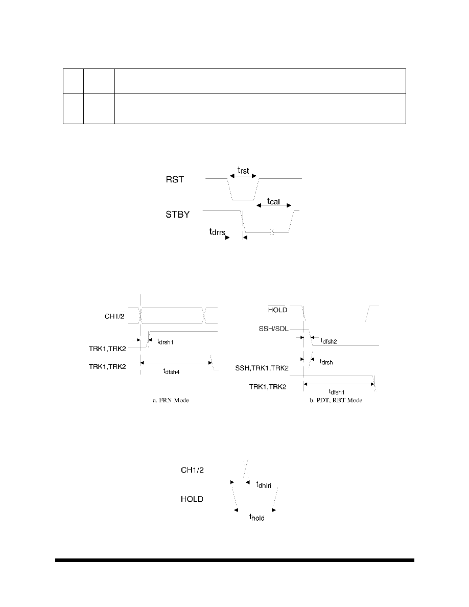
RST Pulse Width
4
t
rst
150
--
--
ns
RST to STBY Falling
t
drrs
--
100
--
ns
RST Rising to STBY Rising
t
cal
--
2,882,040
--
tclk
CH1/2 Edge to TRK1, TRK2 Rising
5
t
drsh1
--
80
--
ns
CH1/2 Edge to TRK1, TRK2 Falling
5
t
dfsh4
--
--
68t
clk
+ 260
ns
HOLD to SSH Falling
6
t
dfsh2
--
60
--
ns
HOLD to TRK1, TRK2, Falling
6
t
dfsh1
66t
clk
--
68t
clk
+ 260
ns
HOLD to TRK1, TRK2, SSH Rising
6
t
drsh
--
120
--
ns
HOLD Pulse Width
7
t
hold
1t
clk
+ 20
--
63t
clk
ns
HOLD to CH1/2 Edge
6
t
dhlri
300
--
64t
clk
ns
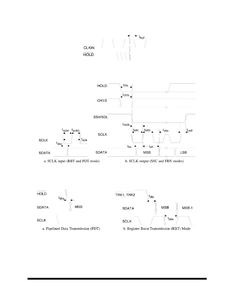
HOLD Falling to CLKIN Falling
7
t
hcf
275
--
1t
clk
+ 10
ns
PDT and RBT Modes
SCLK Input Pulse Period
t
sclk
1000
--
--
ns
SCLK Input Pulse Width Low
t
sckll
500
--
--
ns
SCLK Input Pulse Width High
t
sclkh
500
--
--
ns
SCLK Input Falling to SDATA Valid
t
dss
--
100
150
ns
HOLD Falling to SDATA Valid - PDT Mode
t
dhs
--
140
230
ns
TRK1, TRK2 Falling to SDATA Valid
8
t
dts
--
65
125
ns
FRN and SSC Modes
SCLK Output Pulse Width Low
t
slkl
--
2t
clk
--
t
clk
SCLK Output Pulse Width High
t
slkh
--
2t
clk
--
t
clk
SDATA Valid Before Rising SCLK
t
ss
2t
clk
- 100
--
--
ns
SDATA Valid After Rising SCLK
t
sh
2t
clk
- 100
--
--
ns
SDL Falling to 1st Rising SCLK
t
rsclk
--
2t
clk
--
ns
Last Rising SCLK to SDL Rising
t
rsdl
--
2t
clk
2t
clk
+ 200
ns
HOLD Falling to 1st Falling SCLK
t
hfs
6t
clk
--
8t
clk
+ 200
ns
CH1/2 Edge to 1st Falling SCLK
t
chfs
--
7t
clk
--
t
clk
1. Minimum CLKIN period is 0.625 µ s is FRN mode (20 kHz sample rate).
2. External loading capacitors are required to allow the crystal to oscillate. Maximum crystal frequency is 1.6 MHz in FRN mode
(20 kHz sample rate).
3. With a 2.0 MHz crystal, two 33 pF loading capacitors and a 10 MW parallel resistor.
4. Guaranteed by initial characterization (5102A die).
5. These times are for FRN mode.
6. These times are for PDT and RBT modes.
T
ABLE
4. 5102ALP S
WITCHING
C
HARACTERISTICS
(T
A
= T
MIN
TO
T
MAX
; VA+, VD+ = 5V ± 10%; VA-, VD- = -5V ± 10%; I
NPUTS
: L
OGIC
0 = 0V, L
OGIC
1 = VD+; C
L
= 50
P
F)
P
ARAMETER
S
YMBOL
M
IN
T
YP
M
AX
U
NIT

M
e
m
o
r
y
6
01.17.05 R
EV
3
All data sheets are subject to change without notice
©2005 Maxwell Technologies Inc.
All rights reserved.
5102ALP
16-Bit, 20 KHz A/D Converter
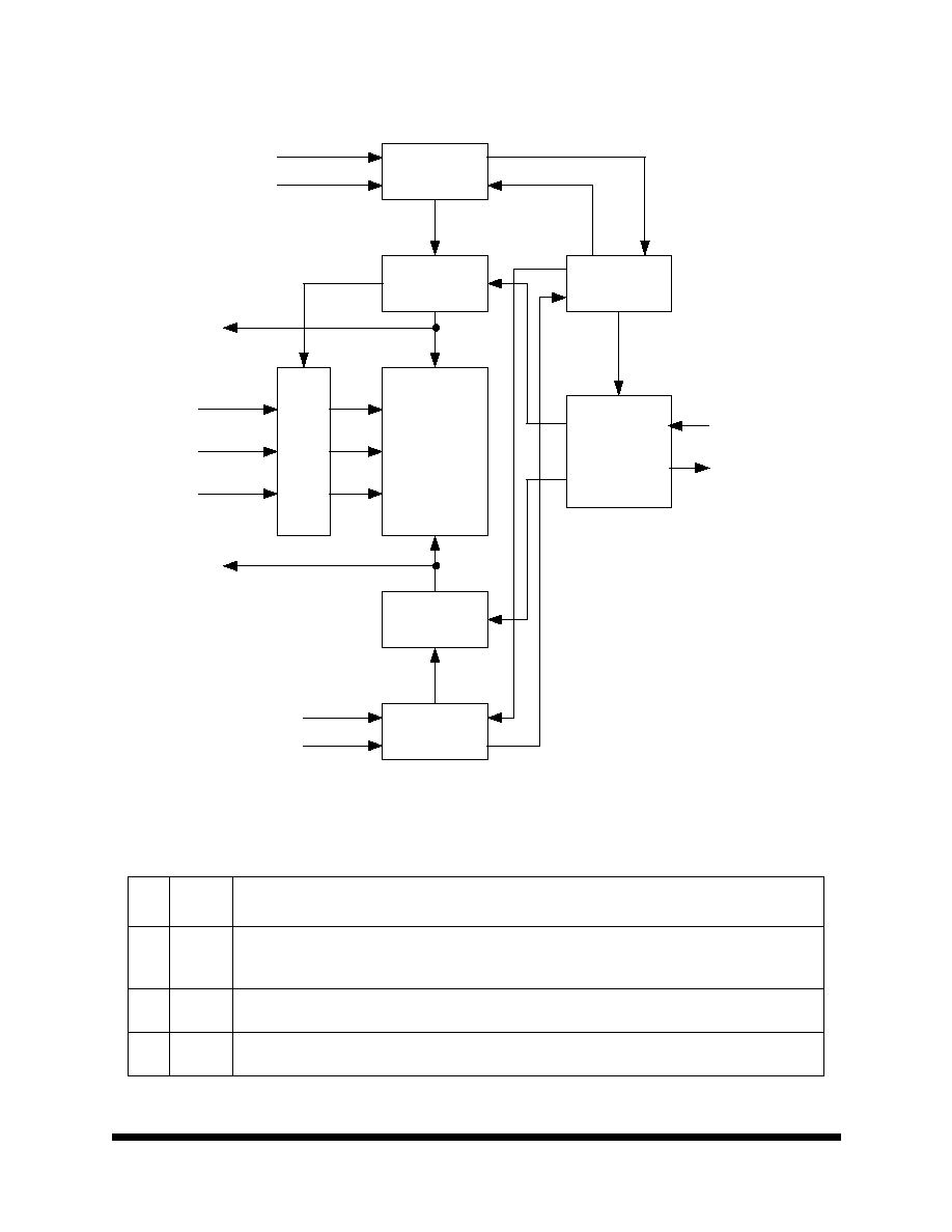
LPTTM O
PERATION
Latchup Protection Technology (LPTTM) automatically detects an increase in the supply current of the 5102ALP con-
verter due to a single event effect and internally cycle the power to the converter off, then on, which restores the
steady state operation of the device.
If data outputs are connected to a bus with other bus driver circuits, all external data bus drivers must be tri-stated and
individual pull up resistors to the supply voltage (if used on the data bus) must no be less than 10 K ohm typical to
assure proper single event effect recovery.
STATUS can also be used to generate an input to the system data processor indicating that an LPTTM cycle has
occurred, and the protected device output accuracy may not be met until after the respective recovery time to the
event. The STATUS signal is generated from an advanced CMOS logic gate output. This output may not exhibit a
monotonic fall time and may even oscillate briefly while power is being restored to the protected device and the decou-
pling capacitance is charged. Loading on the STATUS output should be minimized because this signal is used inter-
nally by the 5102ALP. It is recommended that load current not exceed 2 mA and load capacitance be kept will below
1000 pF.
7. When HOLD goes low, the analog sample is captured immediately. To start conversion, HOLD must be latched by a falling
edge of CLKIN. Conversion will begin on the next rising edge of CLKIN after HOLD is latched.
8. Only valid for TRK1, TRK2 falling when SCLK is low. If SCLK is high when TRK1, TRK2 falls, then SDATA is valid t
dss
time after
the next falling SCLK.
T
ABLE
5. 5102ALP D
IGITAL
C
HARACTERISTICS
(T
A
= T
MIN
TO
T
MA
X; VA+, VD+ = 5V ± 10%; VA-, VD- = -5V ± 10%)
P
ARAMETER
S
YMBOL
M
IN
T
YP
M
AX
U
NIT
Calibration Memory Retention Power Supply Voltage
VA+ & VD+
1
1. VA- and VD- can be any value from zero to -5V for memory retention. Neither VA- or VD- should be allowed to go positive.
AIN1, AIN2 or V
REF
must not be greater than VA+ or VD+. This parameter is guaranteed by characterization.
V
MR
2.0
--
--
V
High-Level Input Voltage
V
IH
2.0
--
--
V
Low-Level Input Voltage
V
IL
--
--
0.8
V
High-Level Output Voltage
2
2. I
OUT
= -100 µ A. This specification guarantees TTL compatibility (V
OH
= 2.4V @ I
OUT
= -40 µ A.
V
OH
(VD+) -1.0
--
--
V
Low-Level Output Voltage - I
OUT
= 1.6 mA
V
OL
--
--
0.4
V
Input Leakage Current
I
IN
--
--
10
µ A
Digital Output Pin Capacitance
C
OUT
--
9
--
pF
M
e
m
o
r
y
7
01.17.05 R
EV
3
All data sheets are subject to change without notice
©2005 Maxwell Technologies Inc.
All rights reserved.
5102ALP
16-Bit, 20 KHz A/D Converter
5102ALP LPT
TM
B
LOCK
D
IAGRAM
L
ATCH
-
UP
P
ROTECTION
C
IRCUIT
(LPT) P
IN
D
ESCRIPTION
P
IN
P
IN
N
AME
F
UNCTION
18
LPTBIT The LPT circuit will crowbar the power supplies to the SEI5102ALPRP for as long as a logi-
cal high is applied. Used to verify operation of the LPT. Normally a logical low or ground is
applied to this input.
26
-LPTV
Negative power supply. VA- and VD- are connected and can be measured on this pin. Nor-
mally -5V.
27
+LPTV Positive power supply. VA+ and VD+ are connected and can be measured on this pin. Nor-
mally +5V.
5102A
Cr
owbar
Switch
Current
Sense
Timer
Control Logic
Switch
Current
Sense
AIN 1
AIN 2
VREF
+VDIG
+VANA
-VDIG
-VANA
+LPTV
-LPTV
LPTBIT
LPTSTATUS
M
e
m
o
r
y
8
01.17.05 R
EV
3
All data sheets are subject to change without notice
©2005 Maxwell Technologies Inc.
All rights reserved.
5102ALP
16-Bit, 20 KHz A/D Converter
.
F
IGURE
1. R
ESET
AND
C
ALIBRATION
T
IMING
F
IGURE
2. C
ONTROL
O
UTPUT
T
IMING
F
IGURE
3. C
HANNEL
S
ELECTION
T
IMING
39
LPT-
STA-
TUS
A 0 to 5V square-wave will output during a latch condition. Normally low.
L
ATCH
-
UP
P
ROTECTION
C
IRCUIT
(LPT) P
IN
D
ESCRIPTION
P
IN
P
IN
N
AME
F
UNCTION
M
e
m
o
r
y
9
01.17.05 R
EV
3
All data sheets are subject to change without notice
©2005 Maxwell Technologies Inc.
All rights reserved.
5102ALP
16-Bit, 20 KHz A/D Converter
F
IGURE
4. S
TART
C
ONVERSION
T
IMING
F
IGURE
5. S
ERIAL
D
ATA
T
IMING
F
IGURE
6. D
ATA
T
RANSMISSION
T
IMING
M
e
m
o
r
y
10
01.17.05 R
EV
3
All data sheets are subject to change without notice
©2005 Maxwell Technologies Inc.
All rights reserved.
5102ALP
16-Bit, 20 KHz A/D Converter
F
IGURE
7. B
YPASS
C
IRCUIT
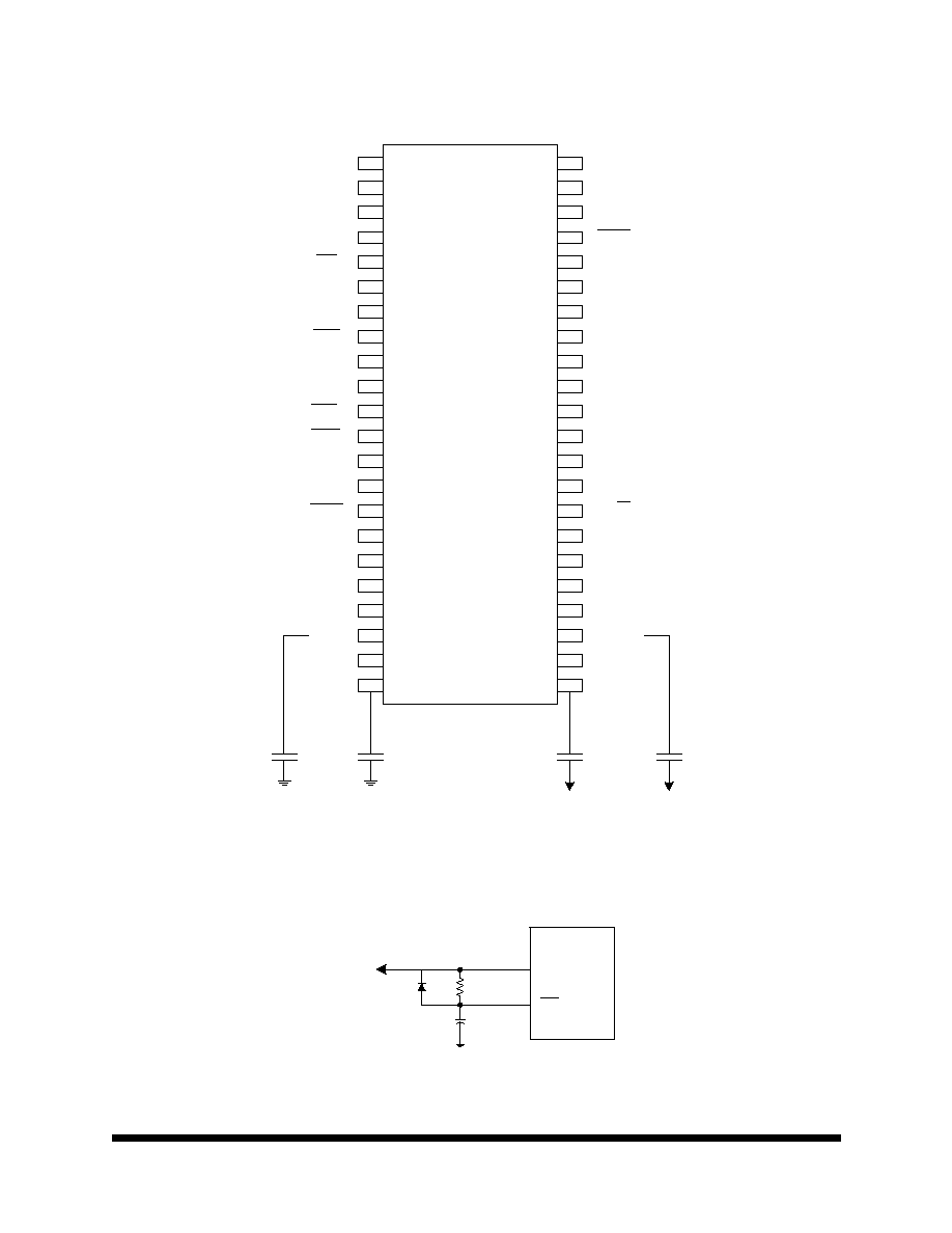
Note:
1. Cap must be connected to the device for proper operation. 4.7 µ F analog side. 1 µ F digital side.
2. Unused logic inputs should be tied to +VD or DGND.
F
IGURE
8. P
OWER
-
UP
R
ESET
C
IRCUIT
1
44
23
22
+VDIG
DGND
-VDIG
RST
CLKIN
XOUT
STBY
DGND
+VDIG
TRK1
TRK2
CRS/FIN
SSH/SDL
HOLD
CH1/2
SCLK
+LPTBIT
NC
-VDIG
-VDIG
DGND
+VDIG
+VANLOG
AGND
-VANLOG
-LPTV
+LPTV
SDATA
CODE
BP/UP
OUTMOD
AIN1
VREF
REFBUF
AGND
-VANLOG
AIN2
+VANLOG
LPTSTATUS
SCKMOD
SLEEP
-VANLOG
AGND
+VANLOG
+
+
+
+
1
µF
1
µF
4.7
µF
4.7
µF
+VD
RST
1N4148
+5V
R
C
M
e
m
o
r
y
11
01.17.05 R
EV
3
All data sheets are subject to change without notice
©2005 Maxwell Technologies Inc.
All rights reserved.
5102ALP
16-Bit, 20 KHz A/D Converter
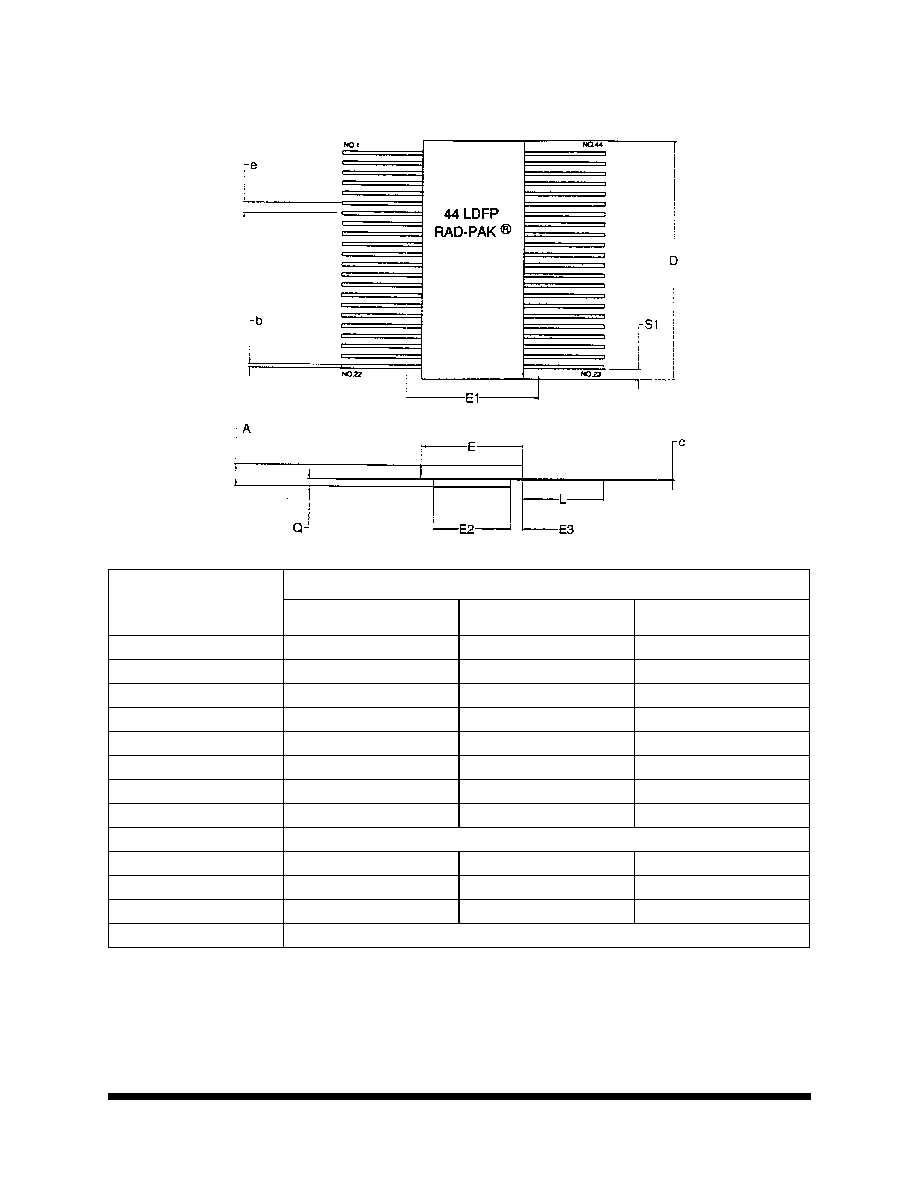
F44
Note: All dimensions in inches
44 P
IN
FRP
S
YMBOL
D
IMENSION
M
IN
N
OM
M
AX
A
0.256
0.282
0.308
b
0.014
0.017
0.020
c
0.009
0.010
0.012
D
1.089
1.100
1.111
E
0.564
0.570
0.576
E1
--
--
0.600
E2
0.410
0.430
0.450
E3
0.044
0.070
--
e
0.050 BSC
L
0.455
0.465
0.475
Q
0.022
0.027
0.032
S1
0.005
--
--
N
44

M
e
m
o
r
y
12
01.17.05 R
EV
3
All data sheets are subject to change without notice
©2005 Maxwell Technologies Inc.
All rights reserved.
5102ALP
16-Bit, 20 KHz A/D Converter
Important Notice:
These data sheets are created using the chip manufacturers published specifications. MAxwell Technologies verifies
functionality by testing key parameters either by 100% testing, sample testing or characterization.
The specifications presented within these data sheets represent the latest and most accurate information available to
date. However, these specifications are subject to change without notice and Maxwell Technologies assumes no
responsibility for the use of this information.
Maxwell Technologies' products are not authorized for use as critical components in life support devices or systems
without express written approval from Maxwell Technologies.
Any claim against MAxwell TechnologiesInc. must be made within 90 days from the date of shipment from Maxwell
Technologies. Maxwell Technologies' liability shall be limited to replacement of defective parts.

M
e
m
o
r
y
13
01.17.05 R
EV
3
All data sheets are subject to change without notice
©2005 Maxwell Technologies Inc.
All rights reserved.
5102ALP
16-Bit, 20 KHz A/D Converter
Product Ordering Options

M
e
m
o
r
y
14
01.17.05 R
EV
3
All data sheets are subject to change without notice
©2005 Maxwell Technologies Inc.
All rights reserved.
5102ALP
16-Bit, 20 KHz A/D Converter
Model Number
5102ALP - RP - F - X
Screening Flow
Multi Chip Module (MCM)
1
K = Maxwell Self-Defined Class K
H = Maxwell Self-Defined Class H
I = Industrial (testing @ -40∞C,
+25∞C, +110∞C)
E = Engineering (testing @ +25∞C)
F = Flat Pack
RP = R
AD
-P
AK
Æ package
16-Bit 20KHz A/D Converter
1) Products are manufactured and screened to Maxwell Technologies self-defined Class H and Class K flows.
Package
Radiation Feature
Base Product
Nomenclature