1
M
e
m
o
r
y
All data sheets are subject to change without notice
(858) 503-3300 - Fax: (858) 503-3301 - www.maxwell.com
Octal Buffers Transceiver
54BCT245
©2002 Maxwell Technologies
All rights reserved.
7.25.02 REV 5
F
EATURES
:
∑ 3-state outputs drive bus lines or buffer memory address
registers
∑ R
AD
-P
AKÆ
radiation-hardened against natural space radia-
tion
∑ Total dose hardness:
- > 100 krad (Si), depending upon space mission
∑ Package:
- 20-pin R
AD
-P
AKÆ
flat package
∑ Operating temperature range: -55 to +125∞C
∑ Bi-CMOS design
∑ ESD protection exceeds 2000V
D
ESCRIPTION
:
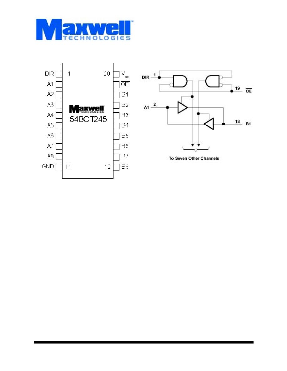
Maxwell Technologies' 54BCT245 octal bus transceiver fea-
tures a greater than 100 krad (Si) total dose tolerance. The
54BCT245 is designed specifically for asynchronous commu-
nication between data buses. The 54BCT245 transmits data
from the A bus to the B bus or from the B bus to the A bus
depending upon the level at the direction-control (DIR) input.
The output-enable (OE) input can be used to disable the
device so the buses are effectively isolated.
Maxwell Technologies' patented R
AD
-P
AK
Æ packaging technol-
ogy incorporates radiation shielding in the microcircuit pack-
age. It eliminates the need for box shielding while providing
the required radiation shielding for a lifetime in orbit or space
mission. In a GEO orbit, R
AD
-P
AK
provides greater than 100
krad (Si) radiation dose tolerance. This product is available
with screening up to Class S.
Logic Diagram

M
e
m
o
r
y
2
All data sheets are subject to change without notice
©2002 Maxwell Technologies
All rights reserved.
Octal Buffers Transceiver
54BCT245
7.25.02 Rev 1
T
ABLE
1. P
INOUT
D
ESCRIPTION
P
IN
S
YMBOL
D
ESCRIPTION
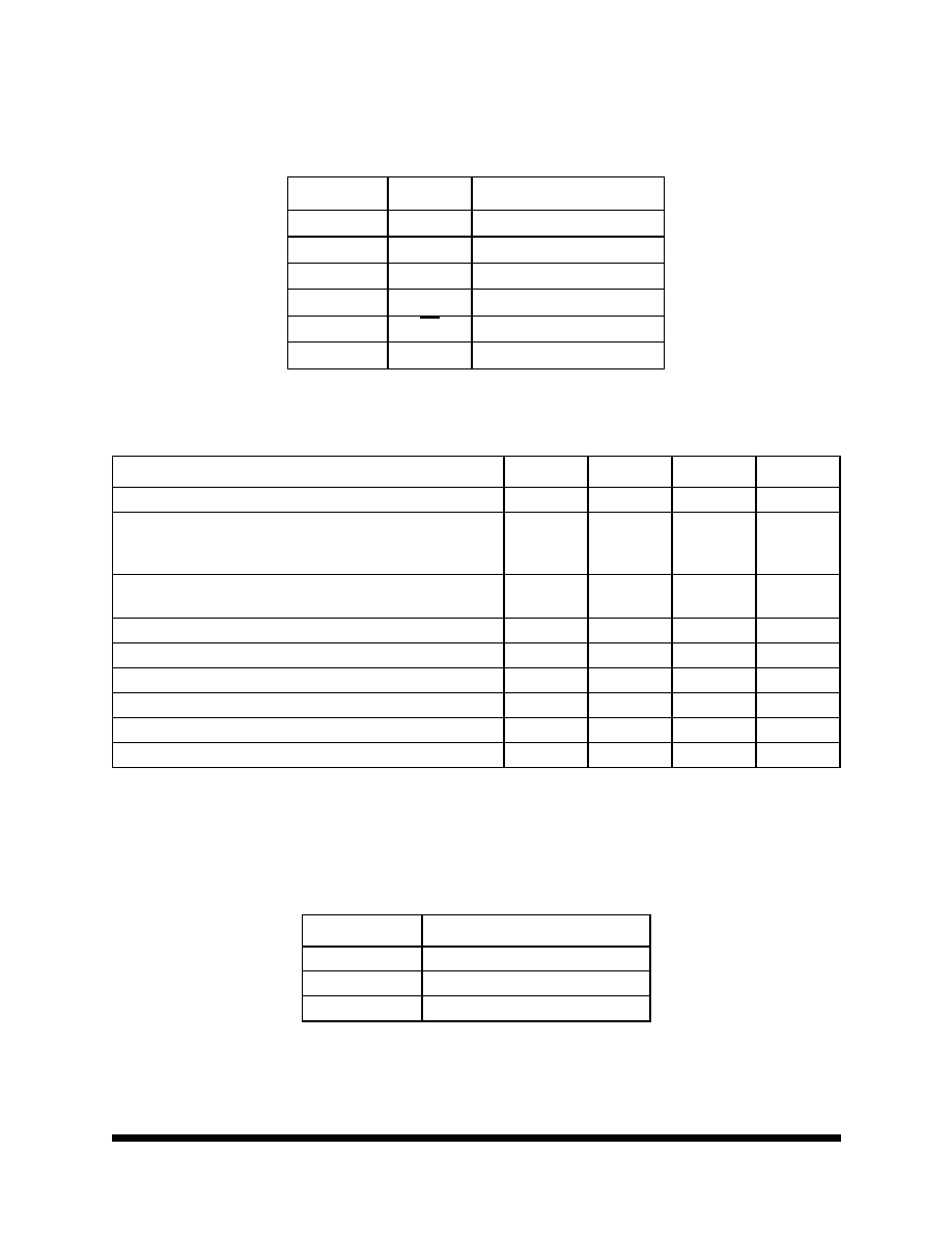
1
DIR
Directional Control Input
2-9
A1-A8
Bi-directional I/O's with Tri-State
10
GND
Ground
11-18
B8-B1
Bi-directional I/O's with Tri-State
19
OE
Output Enable
20
V
CC
Supply Power
T
ABLE
2. 54BCT245 A
BSOLUTE
M
AXIMUM
R
ATINGS
1
1. Stresses above the absolute maximum rating may cause permanent damage to the device. Extended operation at the maxi-
mum levels may degrade performance and affect reliability.
P
ARAMETER
S
YMBOL
M
IN
M
AX
U
NIT
Supply Voltage Range
V
CC
-0.5
7.0
V
Input Voltage Range
Control Input 3/I/O Ports
2
I/O Ports
3
2. The input and output voltage ratings may be exceeded if the input and output current ratings are observed.
V
I
-0.5
-0.5
7.0
5.5
V
Voltage Range Applied to any Output in the Disable or Power-Off
State
V
O
-0.5
7.0
V
Voltage Range Applied to any Output in High State
V
O
-0.5
V
CC
V
Current Into Any Output in the Low State
I
O
--
96
mA
Total Power Dissipation @ T
A
= +55
∞
C
3
3. Must be able to withstand the additional P
D
due to short circuit test, e.g. I
DS
. The P
D
number is based upon dc values.
P
D
--
651
mW
Input Clamp Current
I
IK
(V
I
< 0)
--
-30
mA
Operating Temperature Range
T
A
-55
125
∞C
Storage Temperature Range
T
S
-65
150
∞C
T
ABLE
3. D
ELTA
L
IMITS
P
ARAMETER
V
ARIATION
I
CC(OL)
±10% of specified value in Table 5
I
CC(OH)
±10% of specified value in Table 5
I
CC(OD)
±10% of specified value in Table 5

M
e
m
o
r
y
3
All data sheets are subject to change without notice
©2002 Maxwell Technologies
All rights reserved.
Octal Buffers Transceiver
54BCT245
7.25.02 Rev 1
T
ABLE
4. 54BCT245 R
ECOMMENDED
O
PERATING
C
ONDITIONS1
1. All unused control inputs must be held high or low to ensure proper device operation.
P
ARAMETER
S
YMBOL
M
IN
M
AX
U
NIT
Supply Voltage
V
CC
4.5
5.5
V
High-Level Input Voltage
V
IH
2.0
--
V
Low-Level Input Voltage
V
IL
--
0.8
V
High-Level Output Current
A Port
B Port
I
OH
--
-3
-12
mA
Low-Level Output Current
A Port
B Port
I
OL
--
20
48
mA
Input Clamp Current
I
IK
--
-18
mA
Thermal Impedance -- Flat Package
JC
--
5.56
∞C/W
Operating Temperature
T
A
-55
125
∞
C
T
ABLE
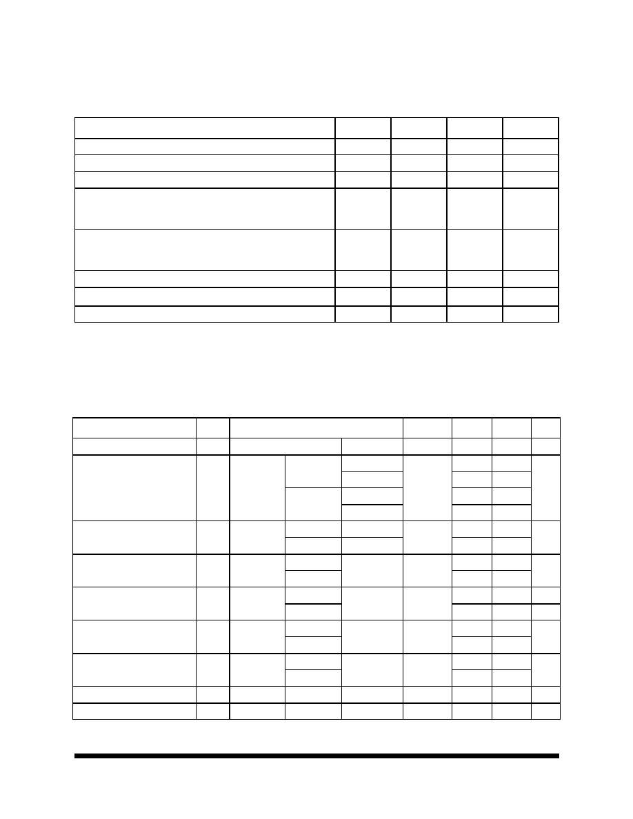
5. 54BCT245 DC E
LECTRICAL
C
HARACTERISTICS
(V
CC
= 5V ±10%, T
A
= -55
∞
C
TO
125
∞
C,
UNLESS
OTHERWISE
SPECIFIED
)
P
ARAMETER
S
YMBOL
T
EST
C
ONDITIONS
S
UBGROUPS
M
IN
M
AX
U
NIT
Input Clamp Voltage
V
IK
V
CC
= 4.5 V
I
I
= -18.0 mA
1, 2, 3
--
-1.2
V
High-Level Output Voltage
V
OH
V
CC
= 4.5 V Port A
I
OH
= -1 mA
1, 2, 3
2.5
--
V
I
OH
= -3 mA
2.4
--
Port B
I
OH
= -3 mA
2.4
--
I
OH
= -12 mA
2
--
Low-Level Output Voltage
V
OL
V
CC
= 4.5 V Port A
I
OL
= 20 mA
1, 2, 3
--
0.5
V
Port B
I
OL
= 48 mA
--
0.55
Input Current
I
I
V
CC
= 5.5 V A or B Port
V
I
= 5.5V
1, 2, 3
1
mA
Control Input
0.1
High Level Input Current
1
I
IH
V
CC
= 5.5 V A or B Port
V
I
= 2.7 V
1, 2, 3
--
70
µ A
Control Input
--
20
µ A
Low Level Input Current
2
I
IL
V
CC
= 5.5 V A or B Port
V
IN
= 0.5 V
1, 2, 3
--
-0.65
mA
Control Input
-1.2
Short-circuit Output Current
2
I
OS
V
CC
= 5.5 V A Port
V
O
= 0 V
1, 2, 3
-60
-150
mA
B Port
-100
-225
Supply Current, Outputs High
I
CCH
A to B
V
CC
= 5.5 V
1, 2, 3
--
57
mA
Supply Current, Outputs Low
I
CCL
A to B
V
CC
= 5.5 V
1, 2, 3
--
90
mA

M
e
m
o
r
y
4
All data sheets are subject to change without notice
©2002 Maxwell Technologies
All rights reserved.
Octal Buffers Transceiver
54BCT245
7.25.02 Rev 1
Supply Current, Outputs Dis-
abled to High Impedance State
I
CCZ
V
CC
= 5.5 V
1, 2, 3
--
15
mA
Input Capacitance
C
i
3
V
I
= 2.5 V or
0.5V
Control Input V
CC
= 5.5 V
1, 2, 3
7
pF
Input Output Capacitance
C
io
3
V
CC
= 5.5 V
A to B
V
I
= 2.5 V or
0.5 V
9
pF
B to A
12
1. For I/O ports, the parameters I
IH
and I
IL
include the off-state output current.
2. Not more than one output should be shorted at one time and the duration of test shall not exceed one second.
3. Guaranteed by design.
T
ABLE
6. 54BCT245 AC E
LECTRICAL
C
HARACTERISTICS
(V
CC
= 5V ±10%, T
A
= -55
∞
C
TO
125
∞
C,
UNLESS
OTHERWISE
SPECIFIED
)
P
ARAMETER
S
YMBOL
T
EST
C
ONDITIONS
S
UBGROUPS
M
IN
M
AX
U
NIT
Propagation Delay Time
from A or B to B or A
t
PLH
V
CC
= 4.5 to 5.5 V
R
1
= 500
C
L
= 50 pF
R
2
= 500
9, 10, 11
1
7.2
ns
t
PHL
T
A
= -55 to +125
∞
C
1.5
7.6
t
PLH
V
CC
= 5.0 V
R
1
= 500
C
L
= 50 pF
R
2
= 500
1
6
t
PHL
T
A
= +25
∞
C
1.5
6.6
Output Enable Time
OE to Yn
t
PZH
V
CC
= 4.5 to 5.5 V
R
1
= 500
C
L
= 50 pF
R
2
= 500
9, 10, 11
1.5
11.2
ns
t
PZL
T
A
= -55 to +125
∞
C
1.5
11.8
t
PZH
V
CC
= 5.0 V
R
1
= 500
C
L
= 50 pF
R
2
= 500
1.5
9.4
t
PZL
T
A
= +25
∞
C
1.5
10.2
Output Disable Time
OE to Yn
t
PHZ
V
CC
= 4.5 to 5.5 V
R
1
= 500
C
L
= 50 pF
R
2
= 500
9, 10, 11
1.5
9.7
ns
t
PLZ
T
A
= -55 to +125
∞
C
1.5
9.6
t
PHZ
V
CC
= 5.0 V
R
1
= 500
C
L
= 50 pF
R
2
= 500
1.5
8.3
t
PLZ
T
A
= +25
∞
C
1.5
7.8
T
ABLE
5. 54BCT245 DC E
LECTRICAL
C
HARACTERISTICS
(V
CC
= 5V ±10%, T
A
= -55
∞
C
TO
125
∞
C,
UNLESS
OTHERWISE
SPECIFIED
)
P
ARAMETER
S
YMBOL
T
EST
C
ONDITIONS
S
UBGROUPS
M
IN
M
AX
U
NIT

M
e
m
o
r
y
5
All data sheets are subject to change without notice
©2002 Maxwell Technologies
All rights reserved.
Octal Buffers Transceiver
54BCT245
7.25.02 Rev 1
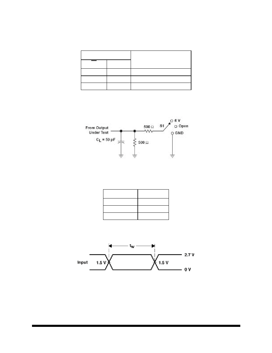
F
IGURE
1. L
OAD
C
IRCUIT
FOR
O
UTPUTS
Figure Note:
1.C
L
includes probe and jig capacitance.
F
IGURE
2. V
OLTAGE
W
AVEFORMS
P
ULSE
D
URATION
T
ABLE
7. F
UNCTION
T
ABLE
INPUTS
OPERATION
OE
DIR
L
L
B data to A bus
L
H
A data to B bus
H
X
Isolation
P
ARAMETER
M
EASUREMENT
I
NFORMATION
T
EST
S1
T
PLH
/T
PHL
Open
T
PLZ
/T
PZL
6V
T
PHZ
/T
PZH
GND
