1
Memory
All data sheets are subject to change without notice
(858) 503-3300 - Fax: (858) 4503-3301 - www.maxwell.com
16-Bit Buffers/Drivers with
54LVTH162244
©2001 Maxwell Technologies.
All rights reserved.
3-State Outputs
12.19.01 Rev 1
1000607
F
EATURES
:
∑ R
AD
-P
AK
Æ radiation-hardened against natural space radia-
tion
∑ Total dose hardness:
- > 100 krad (Si), depending upon space mission
∑ Output ports have equivalent 22-
series resistors, so no
external resistors are required
∑ Support mixed-mode signal operation (5V input and output
voltages with 3.3V V
CC
)
∑ Support unregulated battery operation down to 2.7V
∑ Typical V
OLP
(Output ground bounce) < 0.8V at V
CC
= 3.3V,
T
A
= 25
∞
C
∑ I
OFF
and power-up 3-state support hot insertion
∑ Bus hold on data inputs eliminates the need for external
pull-up/pull-down resistors
∑ Distributed V
CC
and GND pin configuration minimizes high-
speed switching noise
∑ Flow-through architecture optimizes PCB layout
∑ Package: 48 pin R
AD
-P
AK
flat pack
D
ESCRIPTION
:
Maxwell Technologies' 54LVTH162244 devices are 16-bit buff-
ers and line drivers designed for low-voltage (3.3V) V
CC
oper-
ation, but with the capability to provide a TTL interface to a 5V
system environment. These devices can be used as four 4-bit
buffers, two 8-bit buffers, or one 16-bit buffer. These devices
provide true outputs and symmetrical active-low output-enable
(OE) inputs.
The outputs, which are designed to source or sink up to 12
mA, include equivalent 22-
series resistors to reduce over-
shoot and undershoot. Active bus-hold circuitry is provided to
hold unused or floating data inputs at a valid logic level.
Maxwell Technologies' patented R
AD
-P
AK
Æ packaging technol-
ogy incorporates radiation shielding in the microcircuit pack-
age. It eliminates the need for box shielding while providing
the required radiation shielding for a lifetime in orbit or space
mission. In a GEO orbit, R
AD
-P
AK
provides greater than 100
krad (Si) radiation dose tolerance. This product is available
with screening up to Class S.
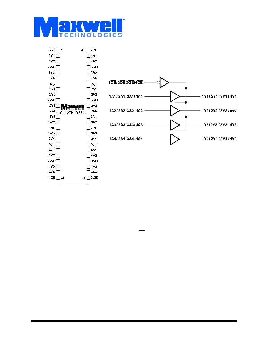
Logic Diagram

Memory
2
All data sheets are subject to change without notice
©2001 Maxwell Technologies.
All rights reserved.
16-Bit Buffers/Drivers with 3-State Outputs
54LVTH162244
12.19.01 Rev 1
1000607
T
ABLE
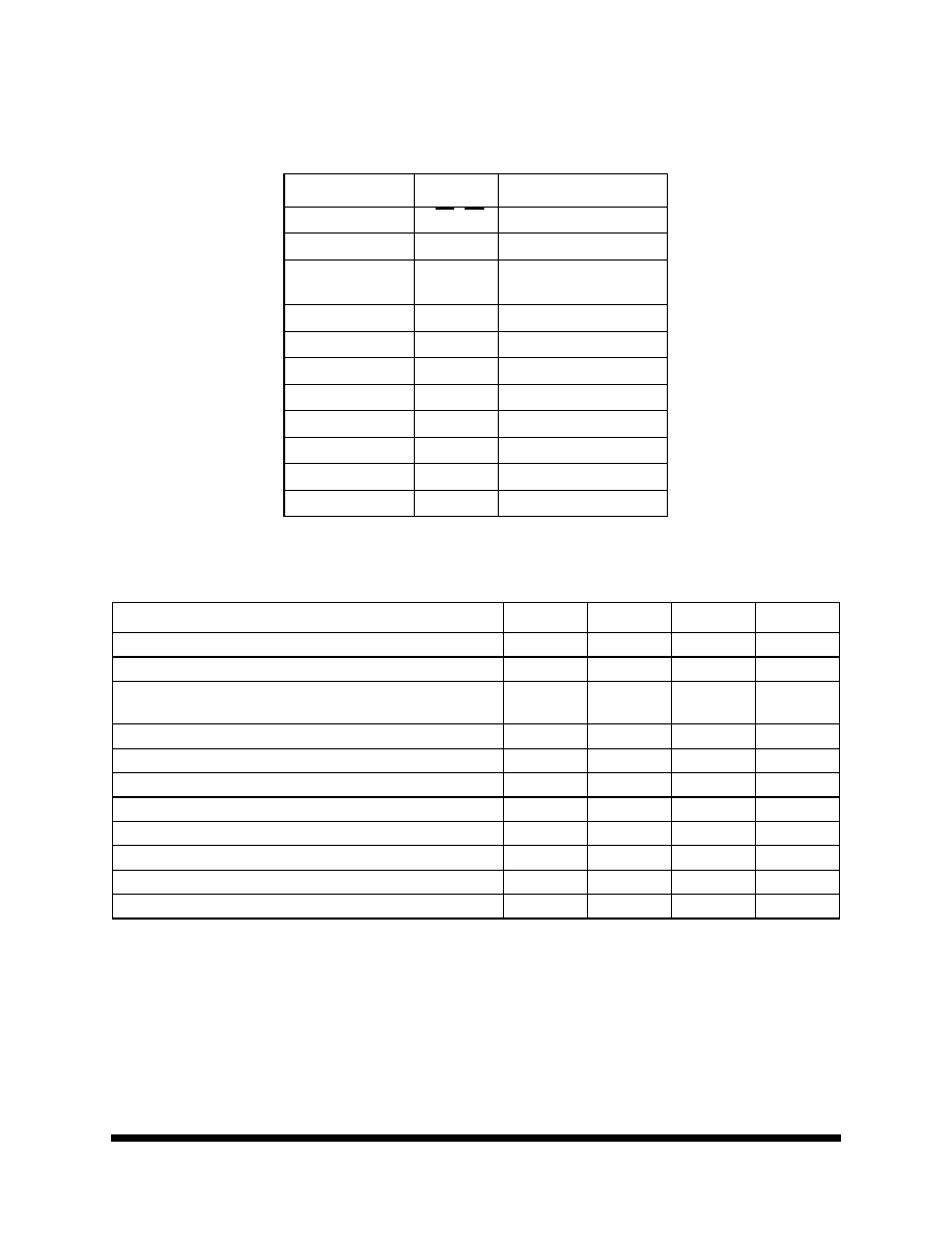
1. P
INOUT
D
ESCRIPTION
P
IN
S
YMBOL
D
ESCRIPTION
1, 48, 25, 24
1OE-4OE
Output Enable
2, 3, 5, 6
1Y1-1Y4
Output
4, 10, 15, 21, 28, 34,
39, 45
GND
Ground
7, 18, 31, 42
V
CC
Supply Voltage
8, 9, 11, 12
2Y1-2Y4
Output
13, 14, 16, 17
3Y1-3Y4
Output
19, 20, 22, 23
4Y1-4Y4
Output
47, 46, 44, 43
1A1-1A4
Input
41, 40, 38, 37
2A1-2A4
Input
36, 35, 33, 32
3A1-3A4
Input
30, 29, 27, 26
4A1-4A4
Input
T
ABLE
2. 162244 A
BSOLUTE
M
AXIMUM
R
ATINGS
1
1. Stresses beyond listed under "absolute maximum ratings" may cause permanent damage to the device. These are stress rat-
ings only and functional operation of the device at these or any other conditions beyond those indicated under "recommended
operating conditions" is not implied. Exposure to absolute-maximum-rated conditions for extended periods may affect device
reliability.
P
ARAMETER
S
YMBOL
M
IN
M
AX
U
NIT
Supply Voltage Range
V
CC
-0.5
4.6
V
Input Voltage Range
2
2. The input and output negative-voltage ratings may be exceeded if the input and output clamp-current ratings are observed.
V
I
-0.5
7
V
Voltage range applied to any output in the high-impedance or
power-off state
2
V
O
-0.5
7
V
Voltage range applied to any output in the high state
2
V
O
-0.5 to V
CC
0.5
V
Current into any output in the low state
I
O
--
30
mA
Current into any output in the high state
3
3. This current flows only when the output is in the high state and V
O
> V
CC
.
I
O
30
--
mA
Input clamp current
I
IK
(V
I
< 0)
--
-50
mA
Output clamp current
I
OK
(V
O
< 0)
--
-50
mA
Operating Temperature
T
A
-55
125
∞C
Storage Temperature Range
T
S
-65
150
∞
C
Operating Temperature Range
T
A
-55
125
∞C

Memory
3
All data sheets are subject to change without notice
©2001 Maxwell Technologies.
All rights reserved.
16-Bit Buffers/Drivers with 3-State Outputs
54LVTH162244
12.19.01 Rev 1
1000607
T
ABLE
3. D
ELTA
L
IMITS
P
ARAMETER
V
ARIATION
I
CC(OP)
±10% of specified value on Table 5
I
OZH
±10% of specified value on Table 5
I
OZL
±10% of specified value on Table 5
T
ABLE
4. 162244 R
ECOMMENDED
O
PERATING
C
ONDITIONS1
1. All unused control inputs of the device must be held at high or low to ensure proper device operation.
P
ARAMETER
S
YMBOL
M
IN
M
AX
U
NIT
Supply Voltage
V
CC
2.7
3.6
V
High-level Input Voltage
V
IH
2
--
V
Low-level Input Voltage
V
IL
--
0.8
V
Input Voltage
V
I
--
5.5
V
High-level output current
I
OH
--
-12
mA
Low-level output current
I
OL
--
12
mA
Input Transition Rise or Fall Rate
Outputs
enabled
t/
v
--
10
ns/V
Power-up ramp rate
t/
V
CC
200
--
µs/V
Operating Temperature
T
A
-55
125
∞
C
T
ABLE
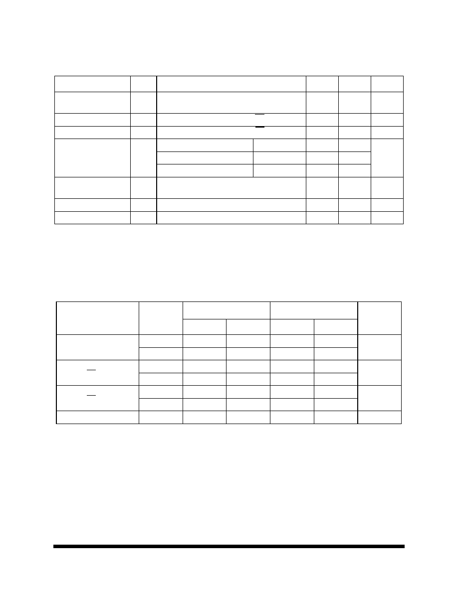
5. 162244 DC E
LECTRICAL
C
HARACTERISTICS
(V
CC
= 3.3V ±10%, T
A
= -55
TO
+125∞C,
UNLESS
OTHERWISE
SPECIFIED
)
P
ARAMETER
S
YMBOL
T
EST
C
ONDITIONS
M
IN
M
AX
U
NIT
Input Clamp Voltage
V
IK
V
CC
= 2.7
I
I
= -18mA
--
-1.2
V
High-Level Output Voltage
V
OH
V
CC
= 3V
I
OH
= -12 mA
2
--
V
Low-Level Output Voltage
V
OL
V
CC
= 3V
I
OL
= 12 mA
--
0.8
V
Input Current
I
I
V
CC
= 0 or 3.6V
VI = 5.5V
--
10
µA
V
CC
= 3.6V
V
I
= V
CC
or
GND
Control inputs
--
±1
V
CC
= 3.6V
V
I
= V
CC
Data Inputs
--
1
V
I
= 0
--
-5
Hold Current
I
I(HOLD)
V
CC
= 3V
V
I
= 0.8V
Data Inputs
75
--
µA
V
I
= 2V
-75
--
Output Disabled Leakage
Current - High
I
OZH
V
CC
= 3.6V, V
O
= 3V
--
5
µA

Memory
4
All data sheets are subject to change without notice
©2001 Maxwell Technologies.
All rights reserved.
16-Bit Buffers/Drivers with 3-State Outputs
54LVTH162244
12.19.01 Rev 1
1000607
Output Disabled Leakage
Current - Low
I
OZL
V
CC
= 3.6V, V
O
= 0.5V
--
-5
µA
Power Up Current
I
OZPU
2
V
CC
= 0 to 1.5V, V
O
= 0.5V to 3V, OE = don't care
--
±100
µA
Power Down Current
I
OZPD
2
V
CC
= 1.5V to 0, V
O
= 0.5V to 3V, OE = don't care
--
±100
µA
Supply Current
I
CC
V
CC
= 3.6V
Outputs high
--
0.19
mA
I
O
= 0
Outputs low
--
5
V
I
= V
CC
or GND
Outputs disabled
--
0.19
Delta Supply Current
I
CC
1
V
CC
= 3V to 3.6V, One input at V
CC
-0.6V, Other inputs
at V
CC
or GND
--
0.2
mA
Input Capacitance
C
I
2
V
I
= 3V or 0
--
8
pF
Input Output Capacitance
C
O
2
V
O
= 3V or 0
--
15
pF
1. This is the increase in supply current for each input that is at the specified TTL voltage level rather than V
CC
or GND.
2. Guaranteed by design.
T
ABLE
6. 162244 AC E
LECTRICAL
C
HARACTERISTICS
(T
A
= -55
TO
+125∞C, C
L
= 50
P
F,
UNLESS
OTHERWISE
SPECIFIED
)
P
ARAMETER
S
YMBOL
V
CC
= 3.3V ±V
V
CC
= 2.7V
U
NIT
M
IN
M
AX
M
IN
M
AX
Propogation Delay Time
A to Y
t
PLH
1.1
4.6
--
5.1
ns
t
PHL
1.1
3.9
--
4.5
Output Enable Time
OE to Y
t
PZH
1.1
5.4
--
6.7
ns
t
PZL
1.3
4.9
--
6.1
Output Disable Time
OE to Y
t
PHZ
1.6
5.9
--
6.5
ns
t
PLZ
1
5.9
--
5.8
Output Skew
t
sk(o)
--
--
--
--
ns
T
ABLE
5. 162244 DC E
LECTRICAL
C
HARACTERISTICS
(V
CC
= 3.3V ±10%, T
A
= -55
TO
+125∞C,
UNLESS
OTHERWISE
SPECIFIED
)
P
ARAMETER
S
YMBOL
T
EST
C
ONDITIONS
M
IN
M
AX
U
NIT

Memory
5
All data sheets are subject to change without notice
©2001 Maxwell Technologies.
All rights reserved.
16-Bit Buffers/Drivers with 3-State Outputs
54LVTH162244
12.19.01 Rev 1
1000607
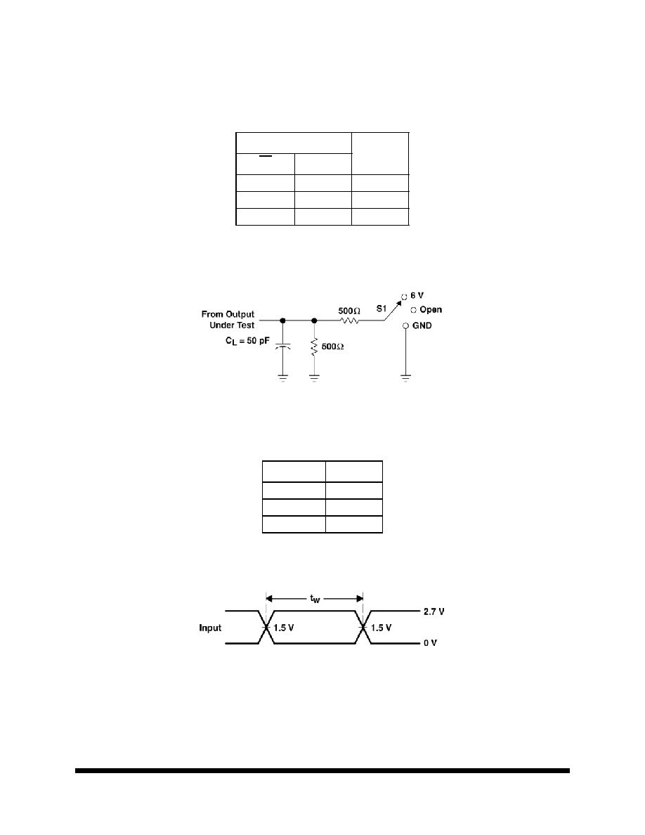
F
IGURE
1. L
OAD
C
IRCUIT
FOR
O
UTPUTS
Figure Note:
1. C
L
includes probe and jog capacitance
.
F
IGURE
2. P
ULSE
D
URATION
T
ABLE
7. F
UNCTION
T
ABLE
(
EACH
4-
BIT
BUFFER
)
INPUTS
OUTPUT
OE
A
Y
L
H
H
L
L
L
H
X
Z
P
ARAMETER
M
EASUREMENT
I
NFORMATION
T
EST
S1
t
PLH
/t
PHL
Open
t
PLZ
/t
PZL
6V
t
PHZ
/t
PZH
GND
