
1
M
e
m
o
r
y
All data sheets are subject to change without notice
(858) 503-3300 - Fax: (858) 503-3301 - www.maxwell.com
16-Bit Bus Transceivers with
54LVTH162245
©2002 Maxwell Technologies
All rights reserved.
3-State Outputs
11.15.02 Rev 2
/
/
/
/
F
EATURES
:
∑ A-Port outputs have equivalent 22-
series resistors, so
no external resistors are required
∑ Support mixed-mode signal operation (5V input and output
voltages with 3.3V V
CC
)
∑ Support unregulated battery operation down to 2.7V
∑ Typical V
OLP
(output ground bounce) < 0.8V at V
CC
= 3.3V,
T
A
= 25
∞
C
∑ I
OFF
and power-up 3-state support hot insertion
∑ Bus hold on data inputs eliminates the need for external
pullup/pulldown resistors
∑ Distributed V
CC
and GND pin configuration minimizes high-
speed switching noise
∑ Flow-through architecture optimizes PCB layout
∑ Total dose hardness:
- > 100 krad (Si), depending upon space mission
∑ Package: 48 pin R
AD
-P
AK
Æ flat pack
D
ESCRIPTION
:
Maxwell Technologies' 54LVTH162245 devices are 16-bit
(dual-octal) non-inverting 3-state transceivers designed for
low-voltage (3.3V) V
CC
operation, but with the capability to
provide a TTL interface to a 5V system environment. These
devices can be used as two 8-bit transceivers or one 16-bit
transceiver. The devices allow data transmission from the A
bus to the B bus or form the B bus to the A bus, depending on
the logic level at the direction-control (DIR) input. The output
enable (OE) input can be used to disable the device so that
the buses are effectively isolated. The A-port outputs, which
are designed to source or sink up to 12 mA, include equivalent
22-
series resistors to reduce overshoot and undershoot.
Maxwell Technologies' patented R
AD
-P
AK
Æ packaging technol-
ogy incorporates radiation shielding in the microcircuit pack-
age. It eliminates the need for box shielding while providing
the required radiation shielding for a lifetime in orbit or space
mission. In a GEO orbit, R
AD
-P
AK
provides greater than 100
krad (Si) radiation dose tolerance. This product is available
with screening up to Class S.
Logic Diagram

M
e
m
o
r
y
2
All data sheets are subject to change without notice
©2002 Maxwell Technologies
All rights reserved.
16-Bit Bus Transceivers with 3-State Outputs
54LVTH162245
11.15.02 Rev 2
.
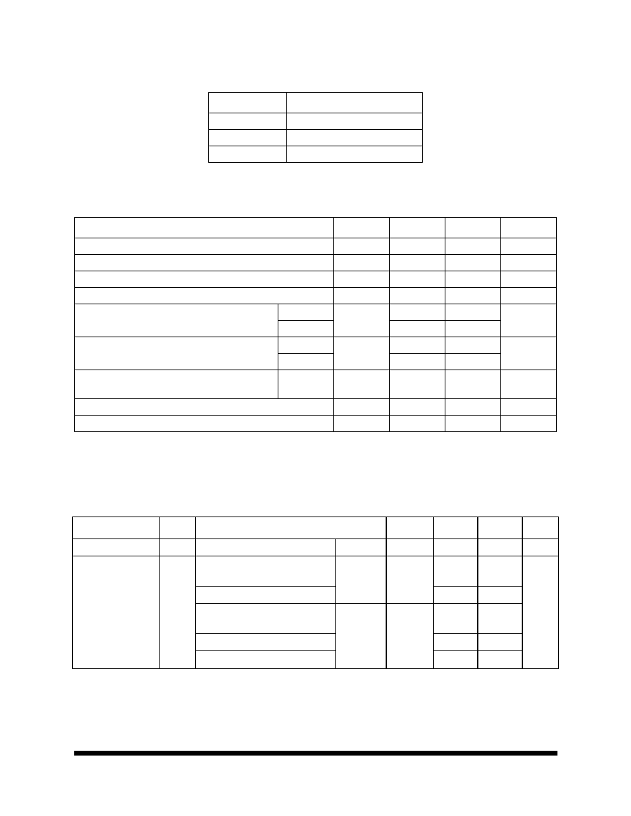
T
ABLE
1. P
INOUT
D
ESCRIPTION
P
IN
S
YMBOL
D
ESCRIPTION
1, 24
1DIR - 2DIR
Direction Control
2, 3, 5, 6, 8, 9, 11, 12
1B1 - 1B8
Output
4, 10, 15, 21, 28, 34, 39, 45
GND
Ground
7, 18, 31, 42
V
CC
Supply Voltage
13, 14, 16, 17, 19, 20, 22, 23
2B - 2B8
Output
25, 48
2OE - 1OE
Output Enable
26, 27, 29, 30, 32, 33, 35, 36
2A8 - 2A1
Input
37, 38, 40, 41, 43, 44, 46, 47
1A8 - 1A1
Input
T
ABLE
2. 54LVTH162245 A
BSOLUTE
M
AXIMUM
R
ATINGS 1
1. Stresses beyond those listed under "absolute maximum ratings" may cause permanent damage to the device. These are
stress ratings only, and functional operation of the device at these or any other conditions beyond those indicated under "rec-
ommended operating conditions" is not implied. Exposure to absolute-maximum-rated conditions for extended periods may
affect device reliability.
P
ARAMETER
S
YMBOL
M
IN
M
AX
U
NIT
Supply voltage range
V
CC
-0.5
4.6
V
Input voltage range
2
2. The input and output negative-voltage ratings may be exceeded if the input and output clamp-current ratings are observed.
V
I
-0.5
7
V
Voltage range applied to any output in the high-impedance or
power-off state
2
V
O
-0.5
7
V
Voltage range applied to any output in the high state
2
V
O
-0.5
V
CC
+ 0.5
V
Current into any output in the low state
B Port
A Port
I
O
--
--
96
30
mA
Current into any output in the high state
3
B Port
A Port
3. This current flows only when the output is in the high state and V
O
> V
CC
.
I
O
--
--
48
30
mA
Input clamp current
I
IK
(V
I
< 0)
-50
--
mA
Output clamp current
I
OK
(V
O
< 0)
-50
--
mA
Thermal resistance
JC
--
5
∞
C/W
Operating temperature range
T
A
-55
125
∞C
Storage temperature range
T
S
-65
150
∞
C
Power Dissipation
PD
--
1
W
M
e
m
o
r
y
3
All data sheets are subject to change without notice
©2002 Maxwell Technologies
All rights reserved.
16-Bit Bus Transceivers with 3-State Outputs
54LVTH162245
11.15.02 Rev 2
T
ABLE
3. D
ELTA
L
IMITS
P
ARAMETER
V
ARIATION
I
CC(OL)
±10% of specified value in Table 5
I
CC(OH)
±10% of specified value in Table 5
I
CC(OD)
±10% of specified value in Table 5
T
ABLE
4. 54LVTH162245 R
ECOMMENDED
O
PERATING
C
ONDITIONS 1
1. All unused control inputs of the device must be held at high or low ensure proper device operation.
P
ARAMETER
S
YMBOL
M
IN
M
AX
U
NIT
Supply voltage
V
CC
2.7
3.6
V
High-level input voltage
V
IH
2
--
V
Low-level input voltage
V
IL
--
0.8
V
Input voltage
V
I
--
5.5
V
High-level output current
A port
I
OH
--
-12
mA
B port
--
-24
Low-level output current
A port
I
OL
--
12
mA
B port
--
48
Input transition rise or fall rate
Outputs
enabled
t/
v
--
10
ns/V
Power-up ramp rate
t/
V
CC
200
--
µ s/V
Operating temperature
T
A
-55
125
∞
C
T
ABLE
5. 54LVTH162245 DC E
LECTRICAL
C
HARACTERISTICS
(V
CC
= 3.3V ±10%, T
A
= -55
TO
+125
∞
C,
UNLESS OTHERWISE SPECIFIED
)
P
ARAMETER
S
YMBOL
T
EST
C
ONDITIONS
S
UBGROUPS
M
IN
M
AX
U
NIT
Input Clamp Voltage
V
IK
V
CC
= 2.7
I
I
= -18 mA
1, 2, 3
--
-1.2
V
High-Level Output
Voltage
V
OH
V
CC
= 2.7V to
3.6V
I
OH
= -100 µ A
A Port
1, 2, 3
V
CC
-0.2
--
V
V
CC
= 3V
I
OH
= -12 mA
2
--
V
CC
= 2.7V to
3.6V
I
OH
= -100 µ A
B Port
1, 2, 3
V
CC
-0.2
--
V
CC
= 2.7V
I
OH
= -8 mA
2.4
V
CC
= 3V,
I
OH
= -24 mA
2

M
e
m
o
r
y
4
All data sheets are subject to change without notice
©2002 Maxwell Technologies
All rights reserved.
16-Bit Bus Transceivers with 3-State Outputs
54LVTH162245
11.15.02 Rev 2
Low-Level Output
Voltage
V
OL
V
CC
= 2.7V to
3.6V
I
OL
= 100 µ A
A Port
1, 2, 3
--
0.2
V
V
CC
= 3V
I
OL
= 12 mA
--
0.8
V
CC
= 2.7V
I
OL
= 100 µ A
B Port
1, 2, 3
--
0.2
I
OL
= 24 mA
--
0.5
V
CC
= 3V
I
OL
= 16 mA
--
0.4
I
OL
= 32 mA
0.5
I
OL
= 48 mA
0.55
Input Current
I
I
V
CC
= 3.6V
VI = VCC or GND
Control
inputs
1, 2, 3
--
±1
µ A
V
CC
= 0 or
3.6V
V
I
= 5.5V
--
10
V
CC
= 3.6V
V
I
= 5.5V
A or B
Ports
1, 2, 3
--
20
V
I
= V
CC
5
V
I
= 0
--
-10
Hold Current
I
I(HOLD)
V
CC
= 3V
V
I
= 0.8V
A Inputs
1, 2, 3
75
--
µ A
V
I
= 2V
-75
--
Power Up Current
I
OZPU
2
V
CC
= 0 to 1.5V, V
O
= 0.5V to 3V, OE = don't care
1, 2, 3
--
±100
µ A
Power Down Current
I
OZPD
2
V
CC
= 1.5V to 0, V
O
= 0.5V to 3V, OE = don't care
1, 2, 3
--
±100
µ A
Supply Current
I
CC
V
CC
= 3.6V
Outputs
high
1, 2, 3
--
0.19
mA
I
O
= 0
Outputs
low
1, 2, 3
--
5
V
I
= V
CC
or GND
Outputs
disabled
1, 2, 3
--
0.19
Delta Supply Current
I
CC
1
V
CC
= 3V to 3.6V, One input at V
CC
-0.6V, Other
inputs at V
CC
or GND
1, 2, 3
--
0.3
mA
Input Capacitance
C
I
2
V
I
= 3V or 0
1, 2, 3
--
8
pF
Input Output Capaci-
tance
C
O
2
V
O
= 3V or 0
1, 2, 3
--
15
pF
1. This is the increase in supply current for each input that is at the specified TTL voltage level rather than V
CC
or GND.
2. Guaranteed by design.
T
ABLE
5. 54LVTH162245 DC E
LECTRICAL
C
HARACTERISTICS
(V
CC
= 3.3V ±10%, T
A
= -55
TO
+125
∞
C,
UNLESS OTHERWISE SPECIFIED
)
P
ARAMETER
S
YMBOL
T
EST
C
ONDITIONS
S
UBGROUPS
M
IN
M
AX
U
NIT
M
e
m
o
r
y
5
All data sheets are subject to change without notice
©2002 Maxwell Technologies
All rights reserved.
16-Bit Bus Transceivers with 3-State Outputs
54LVTH162245
11.15.02 Rev 2
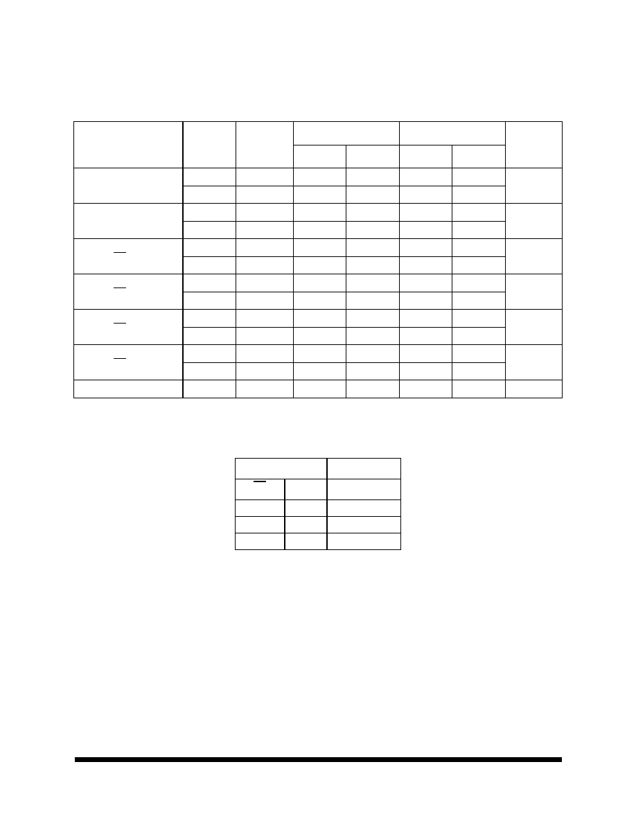
T
ABLE
6. 54LVTH162245 AC E
LECTRICAL
C
HARACTERISTICS
(V
CC
= 3.3V ±10%, T
A
= -55
TO
+125
∞
C,
UNLESS OTHERWISE SPECIFIED
)
P
ARAMETER
S
YMBOL
S
UBGROUPS
V
CC
= 3.3V ± 0.3
V
CC
= 2.7V
U
NIT
M
IN
M
AX
M
IN
M
AX
Propagation Delay Time
A to B
t
PLH
9, 10, 11
1
3.5
--
4
ns
t
PHL
9, 10, 11
1
3.5
--
3.9
Propagation Delay Time
B to A
t
PLH
9, 10, 11
1
4.3
--
5.3
ns
t
PHL
9, 10, 11
1
4.2
--
4.5
Output Enable Time
OE to B
t
PZH
9, 10, 11
1
4.8
--
5.9
ns
t
PZL
9, 10, 11
1
4.8
--
5.5
Output Enable Time
OE to A
t
PZH
9, 10, 11
1
5.5
--
7.2
ns
t
PZL
9, 10, 11
1
5.4
--
6.4
Output Disable Time
OE to B
t
PHZ
9, 10, 11
1
5.5
--
5.8
ns
t
PLZ
9, 10, 11
1
5.5
--
5.8
Output Disable Time
OE to A
t
PHZ
9, 10, 11
1
5.8
--
6.5
ns
t
PLZ
9, 10, 11
1
6.3
--
6.3
Output Skew
t
sk(o)
9, 10, 11
--
--
--
--
ns
T
ABLE
7. F
UNTION
T
ABLE
(
EACH
8-
BIT SECTION
)
INPUTS
OPERATION
OE
DIR
L
L
B data to A bus
l
H
A data to B bus
H
X
Isolation