 | –≠–ª–µ–∫—Ç—Ä–æ–Ω–Ω—ã–π –∫–æ–º–ø–æ–Ω–µ–Ω—Ç: 5675 | –°–∫–∞—á–∞—Ç—å:  PDF PDF  ZIP ZIP |
1
All data sheets are subject to change without notice
(858) 503-3300 - Fax: (858) 503-3301 - www.maxwell.com
14-BIT, 400MSPS
5675
©2004 Maxwell Technologies
All rights reserved.
DIGITAL-TO-ANOALOG CONVERTER
07.13.04 Rev 1X
F
EATURES
:
∑ 400-MSPS Update Rate
∑ LVDS-Compatable Input Interface
∑ Differential Scalable Current Outputs: 2mA to 20mA
∑ On-Chip 1.2-V Reference
∑ Single 3.3-V Supply Operation
∑ Power Dissipation: 820 mW at f
CLK
= 400MHz,
f
O
= 70MHz
D
ESCRIPTION
:
Maxwell Technologies 5675 is a 14-bit resolution high-
speed digital to analog converter. The 5675 is designed
for high-speed digital data transmission in wired and
wireless communication systems. The 5675 has exce-
lent spurios free dynamic range (SFDR) at high interme-
diate frequencies.
The 5675 operates from a single-supply voltage of 3.3V.
Power dissipation is 820 mW at fclk = 400 MSPS, fout =
70MHz. The 5675 provides a nominal full-scale differen-
tial current output of 20mA, supporting both single-
ended and differential applications. Theoutput can be
directly fed to the load with no additional external output
buffered required.
Maxwell Technologies' patented R
AD
-P
AK
Æ packaging
technology incorporates radiation shielding in the micro-
circuit package. It eliminates the need for box shielding
while providing the required radiation shielding for a life-
time in orbit or space mission. In a GEO orbit, R
AD
-P
AK
Æ
provides greater than 100 krad(Si) radiation dose toler-
ance. This product is available with screening up to
Class S.
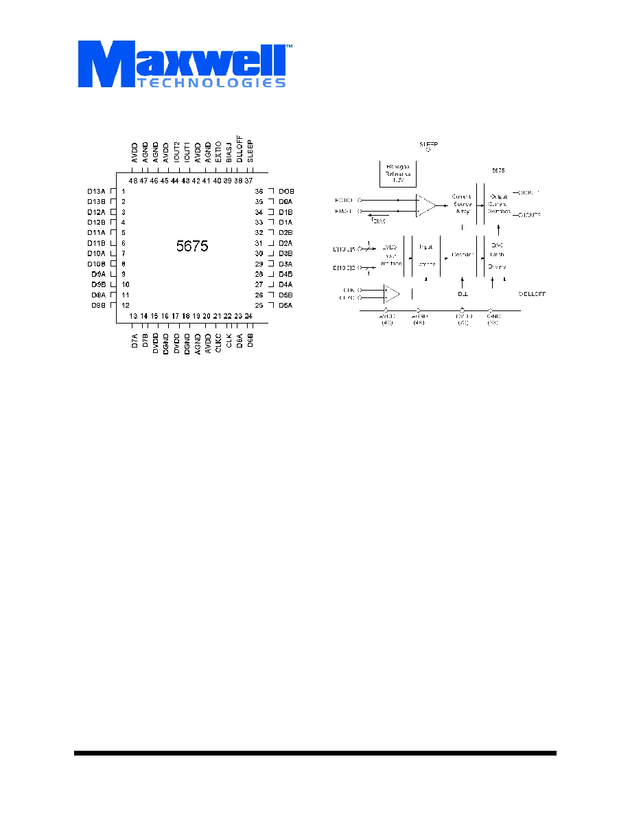
Functional Block Diagram

M
e
m
o
r
y
2
All data sheets are subject to change without notice
©2004 Maxwell Technologies
All rights reserved.
14-BIT, 400MSPS DIGITAL-TO-ANALOG Converter
5675
07.13.04 Rev 1
T
ABLE
1. P
INOUT
D
ESCRIPTION
P
IN
S
YMBOL
D
ESCRIPTION
19, 41, 46, 47
AGND
Analog Negative Supply Voltage (Ground)
20, 42, 45, 48
AVDD
Analog Positive Supply Voltage
39
BIASJ
Full-scale Output Current Bias
22
CLK
External Clock Input
21
CLKC
Complementory External Clock Input
1, 3, 5, 7, 9, 13, 23
25, 27, 29, 31, 33, 35
D9(13:0)A
LVDS Positive Input, data bits 13 through 0
D13A is most significant data bit (MSB)
D0A is the least significant bit (LSB)
2, 4, 6, 8, 10, 14, 24
26, 28, 30, 32, 34, 36
D(13:0)B
LVDS Positive Input, data bits 13 through 0
D13B is most significant data bit (MSB)
D0B is the least significant bit (LSB)
16, 18
DGND
Digital Negative Supply Voltage (Ground)
38
DLLOFF
High = DLL Off / Low = DLL On
15, 17
DVDD
Digital Positive Supply Voltage
40
EXTIO
Internal reference out put or external reference input. Requires a 0.1uf decou-
pling capacitor to groind when used as reference output.
43
IOUT1
DAC current output. Full scale when all inputs are set to 1. Connect reference
side DAC load resistors to AVDD
44
IOUT2
DAC complimentory current output. Full scale when all inputs are set to 0.
Connect reference side DAC load resistors to AVDD
37
SLEEP
Asynchronous hardware power down input. Active high. Internally pulldown.
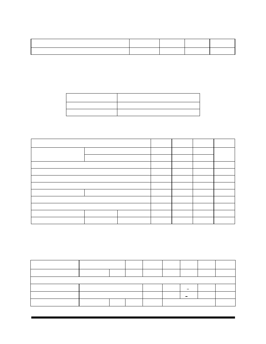
T
ABLE
2. 5675 A
BSOLUTE
M
AXIMUM
R
ATINGS
1
P
ARAMETER
S
YMBOL
M
IN
M
AX
U
NIT
Supply Voltage Range
AV
DD
-0.3
3.6
V
DV
DD
-0.3
3.6
V
AV
DD
to
DV
DD
-3.6
3.6
V
Voltage between AGND and DGND
--
-0.3
0.5
V
CLK, CLKC, SLEEP
--
-0.3 to DVDD
DVDD to 0.3
V
Digital input D[13:0]A, D[13:0]B
--
-0.3 to DVDD
DVDD to 0.3
V
IOUT1, IOUT2
--
-1.0 to DVDD
AVDD to 0.3
V
EXTIO, BIASJ
--
-0.3 to DVDD
AVDD to 0.3
V
Peak Input Current (any input)
20
mA
Peak Total Input Current (any input)
-30
mA
Storage temperature range
-65
150
∞
C
M
e
m
o
r
y
3
All data sheets are subject to change without notice
©2004 Maxwell Technologies
All rights reserved.
14-BIT, 400MSPS DIGITAL-TO-ANALOG Converter
5675
07.13.04 Rev 1
Operating Temperature range
-55
125
∞
C
1. Stresses beyond those listed under "absolute maximum ratings" may cause permanent damage to the device. These are stress
ratings only, and functional operation of the device at these or any other conditions beyond those indicated under "recom-
mended operating conditions" is not implied. Exposure to absolute-maximum-rated conditions for extended periods may affect
device reliability.
T
ABLE
3. D
ELTA
L
IMITS
P
ARAMETER
V
ARIATION
I
AVDD
±10% of specified value in Table 5
I
DVDD
±10% of specified value in Table 5
T
ABLE
4. 5675 R
ECOMMENDED
O
PERATING
C
ONDITIONS
1
1. All unused control inputs of the device must be held at high or low ensure proper device operation.
P
ARAMETER
M
IN
T
YP
M
AX
U
NIT
Output Update Rate
DLL disable, DLLOFF=1
100
MSPS
DLL enable, DLLOFF=0
100
400
Analog Supply Voltage, AVDD
3.15
3.3
3.6
V
Digital Supply Voltage, DVDD
3.15
3.3
3.6
V
Input Reference Voltage, EXTIO
0.6
1.2
1.25
V
Full-scale output currentm IO(FS)
2
20
mA
Output compliance range
AVDD=3.15 to 3.45V, IO(FS)=20mA
AVDD-1
AVDD+0.3
V
Clock Differential Input Votage, CLK-CLKC
0.4
0.8
V
Clock Pulse Width High, tWH
1.25
nS
Clock Pulse Width Low, tLH
1.25
nS
Clock Duty Cycle
40
60
%
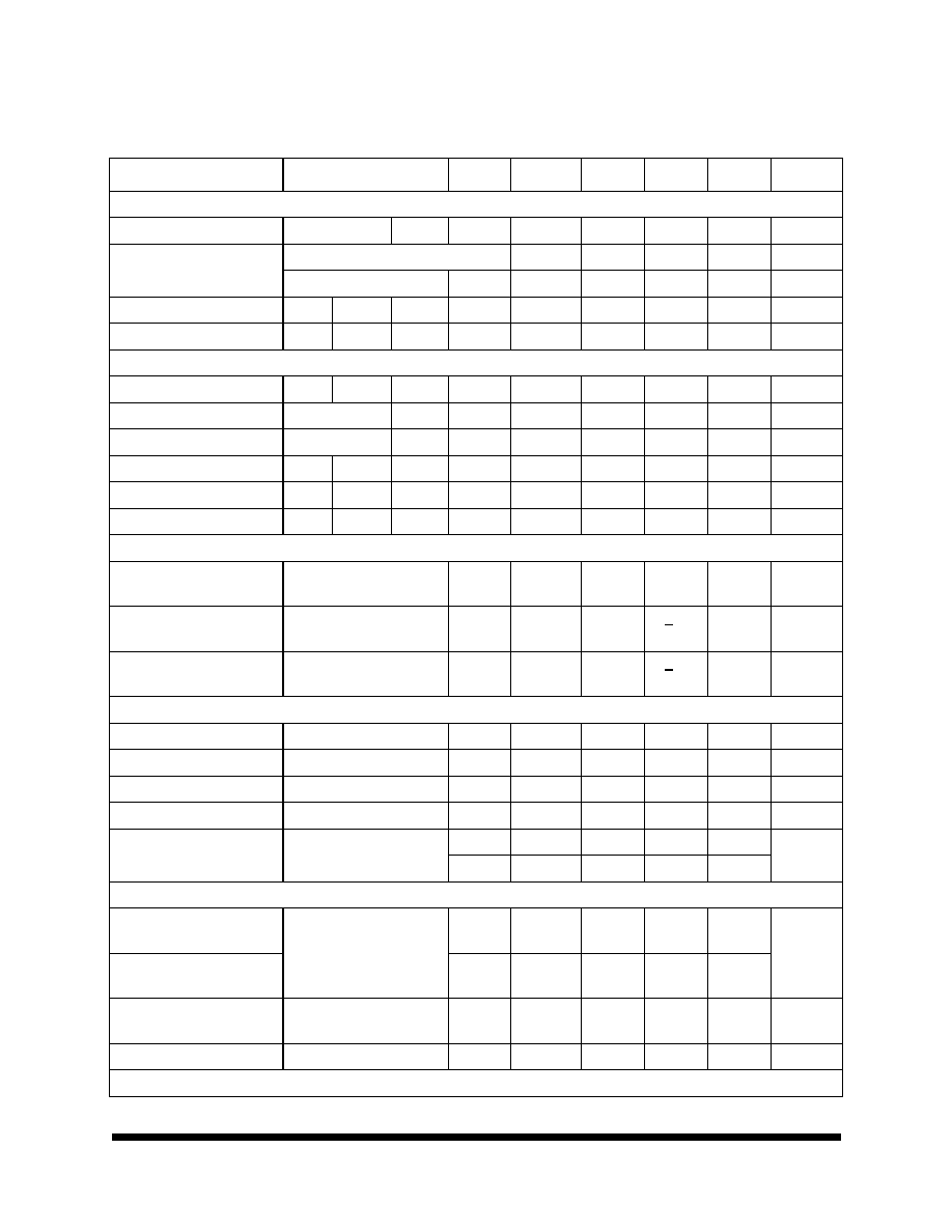
T
ABLE
5. 5675 DC E
LECTRICAL
C
HARACTERISTICS
(DVDD = 3.3±10%, AVDD = 3.3±10%, T
A
= -55
TO
+125
∞
C,
UNLESS
OTHERWISE
SPECIFIED
)
P
ARAMETER
T
EST
C
ONDITIONS
S
YMBLE
S
UBGROUPS
M
IN
T
YP
M
AX
U
NIT
Resolution
14
Bits
DC Accuracy
1
Integral Nonlinearity
T
MIN
TO
T
MAX
INL
-4
+2
4
LSB
D
IFFERENTIAL
N
ONLINEARITY
T
MIN
TO
T
MAX
DNL
-2
+1.5
2
LSB
M
ONOTICITY
Monotonic 12-bit Level
T
ABLE
2. 5675 A
BSOLUTE
M
AXIMUM
R
ATINGS
1
P
ARAMETER
S
YMBOL
M
IN
M
AX
U
NIT
M
e
m
o
r
y
4
All data sheets are subject to change without notice
©2004 Maxwell Technologies
All rights reserved.
14-BIT, 400MSPS DIGITAL-TO-ANALOG Converter
5675
07.13.04 Rev 1
A
NALOG
O
UTPUT
O
FFSET
E
RROR
0.02
%FSR
G
AIN
E
RROR
Without Internal Reference
-10
10
%FSR
With Internal Reference
-10
10
%FSR
O
UTPUT
R
ESISTANCE
300
K
O
UTPUT
C
APACITANCE
5
pf
R
EFERENCE
O
UTPUT
R
EFERENCE
V
OLTAGE
EXTIO
1.17
1.23
1.29
V
R
EFERENCE
O
UTPUT
C
URRENT2
100
nA
R
EFERENCE
I
NPUT
I
NPUT
R
ESISTANCE
1
M
S
MALL
S
IGNAL
B
ANDWIDTH
1.4
MHz
I
NPUT
C
APACITANCE
100
pf
T
EMPERATURE
C
OEFFICIENTS
O
FFSET
D
RIFT
0
ppm of
FSR/
∞
C
G
AIN
D
RIFT
Without Internal Reference
+50
ppm of
FSR/
∞
C
R
EFERENCE
V
OLTAGE
D
RIFT
V
EXTIO
+50
ppm of
FSR/
∞
C
P
OWER
S
UPPLY
A
NALOG
S
UPPLY
C
URRENT3
I
AVDD
175
mA
D
IGITAL
S
UPPLY
C
URREN3T
I
DVDD
100
mA
A
NALOG
S
UPPLY
C
URRENT4
Sleep Mode
I
AVDD
45
mA
P
OWER
D
ISSIPATION
AVdd = 3.3V, DVdd = 3.3V
P
D
A
NALOG
AND
D
IGITAL
POWER
SUPPLY
REJECTION
RATIO
AVdd = 3.15 to 3.45V
A
PSRR
-0.5
0.5
%FSm
WR/V
D
PSRR
-0.5
0.5
LVDS I
NTERFACE
:
NODE
D[13:0]A; D[13:0]B
P
OSITIVE
-
GOING
DIFFERENTIAL
INPUT
VOLTAGE
THRESHOLD
See LVDS min/max
threshold voltage table
V
ITH
+
100
mV
N
EGATIVE
-
GOING
DIFFERENTIAL
INPUT
VOLTAGE
THRESHOLD
V
ITH
-
-100
I
NTERNAL
T
ERMINATION
I
MPEDANCE
Z
T
90
132
Ohms
I
NPUT
C
APACITANCE
C
I
2
pF
CMOS I
NTERFACE
:
NODE
SLEEP
T
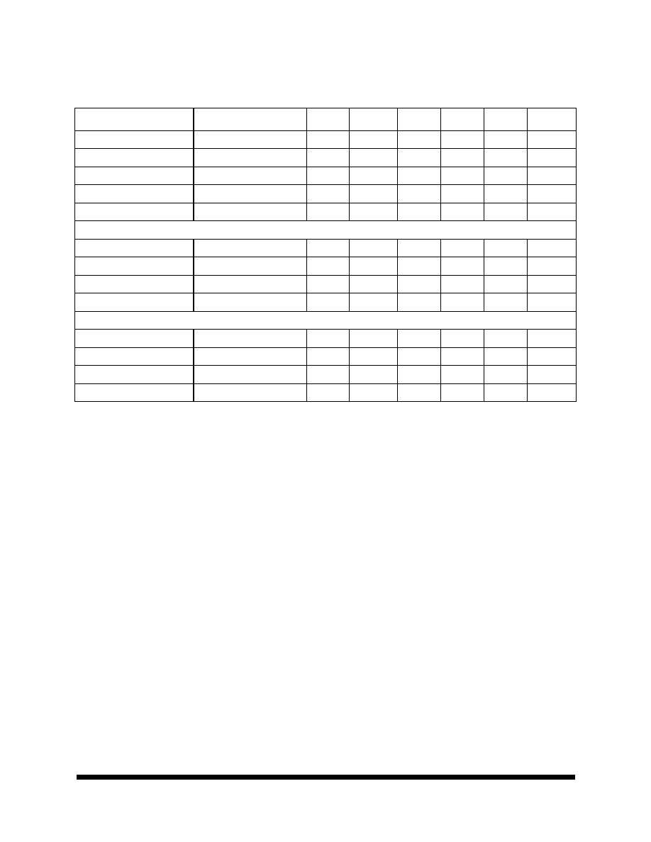
ABLE
5. 5675 DC E
LECTRICAL
C
HARACTERISTICS
(DVDD = 3.3±10%, AVDD = 3.3±10%, T
A
= -55
TO
+125
∞
C,
UNLESS
OTHERWISE
SPECIFIED
)
P
ARAMETER
T
EST
C
ONDITIONS
S
YMBLE
S
UBGROUPS
M
IN
T
YP
M
AX
U
NIT
M
e
m
o
r
y
5
All data sheets are subject to change without notice
©2004 Maxwell Technologies
All rights reserved.
14-BIT, 400MSPS DIGITAL-TO-ANALOG Converter
5675
07.13.04 Rev 1
H
IGH
-L
EVEL
INPUT
VOLTAGE
V
IH
2
3.3
V
L
OW
-L
EVEL
INPUT
VOLTAGE
V
IL
0
0.8
V
H
IGH
-L
EVEL
INPUT
CURRENT
I
IH
-10
10
uA
L
OW
-L
EVEL
INPUT
CURRENT
I
IL
-10
10
uA
I
NPUT
CAPACITANCE
2
pF
C
LOCK
INTERFACE
:
NODE
CLK, CLCKC
I
NPUT
R
ESISTANCE
node CLK, CLKC
670
Ohms
I
NPUT
C
APACITANCE
node CLK, CLKC
2
pF
I
NPUT
R
ESISTANCE
Differential
1.3
Kohms
I
NPUT
C
APACITANCE
Differential
1
pF
T
IMING
I
NPUT
S
ETUP
T
IME
t
SU
1.5
nS
I
NPUT
H
OLD
T
IME
t
h
0.25
nS
I
NPUT
L
ATCH
PULSE
HIGH
TIME
TLPH
2
nS
D
IGITAL
D
ELAY
T
IME
TDD
1
clk
1. Measured Differential at IOUT1 and IOUT2. 2.5Ohms to AVDD
2. Use an external buffer amplifier with high impedance input drive to drive any external load.
3. Measured at f
CLK
= 400 MSPS and F
OUT
= 70 MHz
4. Measured for 50 Ohms Rl at IOUT1 and IOUT2, f
CLK
= 400 MSPS and f
OUT
= 70MHz
T
ABLE
5. 5675 DC E
LECTRICAL
C
HARACTERISTICS
(DVDD = 3.3±10%, AVDD = 3.3±10%, T
A
= -55
TO
+125
∞
C,
UNLESS
OTHERWISE
SPECIFIED
)
P
ARAMETER
T
EST
C
ONDITIONS
S
YMBLE
S
UBGROUPS
M
IN
T
YP
M
AX
U
NIT