REVISIONS
LTR
DESCRIPTION
DATE
(YR-MO-DA)
APPROVED
A
Add packages T and W. Add vendor CAGE 60395 as source of
supply. Increase data retention to 20 years, minimum. Redrawn with
changes.
93-06-29
M. A. Frye
B
Changes in accordance with NOR 5962-R139-94.
94-03-29
M. A. Frye
C
Changes in accordance with NOR 5962-R278-94.
94-09-19
M. A. Frye
D
Changes in accordance with NOR 5962-R163-96.
96-06-27
M. A. Frye
E
Updated boilerplate. Added device types 16-18 and packages M and N
to drawing along with vendor CAGE 0EU86 as supplier. Removed
figures 9, 10 and 11 software data protect algorithms. Removed
vendor 61395 as supplier. - glg
98-07-22
Raymond Monnin
F
Corrected dimensions for packages "M" and "N". - glg
99-10-06
Raymond Monnin
G
Added device 19, packages 6 and 7, and updated boilerplate. ksr
01- 10- 05
Raymond Monnin
THE ORIGINAL FIRST PAGE OF THIS DRAWING HAS BEEN REPLACED.
REV
G
G
G
SHEET
35
36
37
REV
G
G
G
G
G
G
G
G
G
G
G
G
G
G
G
G
G
G
G
G
SHEET
15
16
17
18
19
20
21
22
23
24
25
26
27
28
29
30
31
32
33
34
REV STATUS
OF SHEETS
REV
G
G
G
G
G
G
G
G
G
G
G
G
G
G
SHEET
1
2
3
4
5
6
7
8
9
10
11
12
13
14
PMIC N/A
PREPARED BY
Kenneth Rice
DEFENSE SUPPLY CENTER COLUMBUS
COLUMBUS, OHIO 43216
STANDARD
MICROCIRCUIT
DRAWING
THIS DRAWING IS
AVAILABLE
FOR USE BY ALL
DEPARTMENTS
AND AGENCIES OF THE
DEPARTMENT OF DEFENSE
AMSC N/A
CHECKED BY
Charles Reusing
MICROCIRCUIT, MEMORY, DIGITAL,
CMOS 128K x 8 BIT EEPROM,
MONOLITHIC SILICON
APPROVED BY
Charles E. Besore
DRAWING APPROVAL DATE
91-07-12
SIZE
A
CAGE CODE
67268
5962-38267
REVISION LEVEL
G
SHEET 1 OF 37
DSCC FORM 2233
APR 97
5962-E561-01
DISTRIBUTION STATEMENT A. Approved for public release; distribution is unlimited.

STANDARD
MICROCIRCUIT DRAWING
DEFENSE SUPPLY CENTER COLUMBUS
COLUMBUS, OHIO 43216-5000
SIZE
A
5962-38267
REVISION LEVEL
G
SHEET
2
DSCC FORM 2234
APR 97
1. SCOPE
1.1 Scope. This drawing documents two product assurance class levels consisting of high reliability (device classes Q and M)
and space application (device class V). A choice of case outlines and lead finishes are available and are reflected in the Part or
Identifying Number (PIN). When available, a choice of Radiation Hardness Assurance (RHA) levels are reflected in the PIN.
1.2 PIN. The PIN shall be as shown in the following example:
5962 - 38267
01
Q
X
X
|
|
|
|
|
|
|
|
|
|
|
|
|
|
|
|
|
|
Federal
RHA
Device
Device
Case
Lead
stock class
designator
type
class
outline
finish
designator
(see 1.2.1)
(see 1.2.2)
designator
(see 1.2.4)
(see 1.2.5)
\ /
(see 1.2.3)
\/
Drawing number
1.2.1 RHA designator. Device classes Q and V RHA marked devices meet the MIL-PRF-38535 specified RHA levels and
are marked with the appropriate RHA designator. Device class M RHA marked devices meet the MIL-PRF-38535, appendix A
specified RHA levels and are marked with the appropriate RHA designator. A dash (-) indicates a non-RHA device.
1.2.2 Device type(s). The device type(s) shall identify the circuit function as follows:
Software
Generic
data
Device type
number
Circuit function
Access time
Write speed
Write mode
Endurance
protect
01,16
1/
128K x 8 EEPROM
250 ns
10 ms
Byte/Page
10,000 cycle
yes
02
128K x 8 EEPROM
250 ns
5 ms
Byte/Page
10,000 cycle
yes
03,17
128K x 8 EEPROM
200 ns
10 ms
Byte/Page
10,000 cycle
yes
04
128K x 8 EEPROM
200 ns
5 ms
Byte/Page
10,000 cycle
yes
05,18
128K x 8 EEPROM
150 ns
10 ms
Byte/Page
10,000 cycle
yes
06
128K x 8 EEPROM
150 ns
5 ms
Byte/Page
10,000 cycle
yes
07,19
128K x 8 EEPROM
120 ns
10 ms
Byte/Page
10,000 cycle
yes
08
128K x 8 EEPROM
120 ns
3 ms
Byte/Page
10,000 cycle
yes
09
128K x 8 EEPROM
90 ns
10 ms
Byte/Page
10,000 cycle
yes
10
128K x 8 EEPROM
90 ns
3 ms
Byte/Page
10,000 cycle
yes
11
128K x 8 EEPROM
70 ns
10 ms
Byte/Page
10,000 cycle
yes
12
128K x 8 EEPROM
70 ns
3 ms
Byte/Page
10,000 cycle
yes
13
128K x 8 EEPROM
120 ns
3 ms
Byte/Page
10,000 cycle
yes
14
128K x 8 EEPROM
90 ns
3 ms
Byte/Page
10,000 cycle
yes
15
128K x 8 EEPROM
70 ns
3 ms
Byte/Page
10,000 cycle
yes
1.2.3 Device class designator. The device class designator shall be a single letter identifying the product assurance level as
follows:
Device class
Device requirements documentation
M
Vendor self-certification to the requirements for MIL-STD-883 compliant, non-JAN
class level B microcircuits in accordance with MIL-PRF-38535, appendix A
Q or V
Certification and qualification to MIL-PRF-38535
1/ Generic numbers are listed on the Standard Microcircuit Drawing Source Approval Bulletin at the end of this document and will
also be listed in QML-38535 and MIL-HDBK-103.

STANDARD
MICROCIRCUIT DRAWING
DEFENSE SUPPLY CENTER COLUMBUS
COLUMBUS, OHIO 43216-5000
SIZE
A
5962-38267
REVISION LEVEL
G
SHEET
3
DSCC FORM 2234
APR 97
1.2.4 Case outline(s). The case outline(s) shall be as designated in MIL-STD-1835 and as follows:
Outline letter Descriptive designator Terminals Package style
X
GDIP1-T32 or CDIP2-T32
32
Dual in-line
Y
CQCC1-N44
44
Square chip carrier
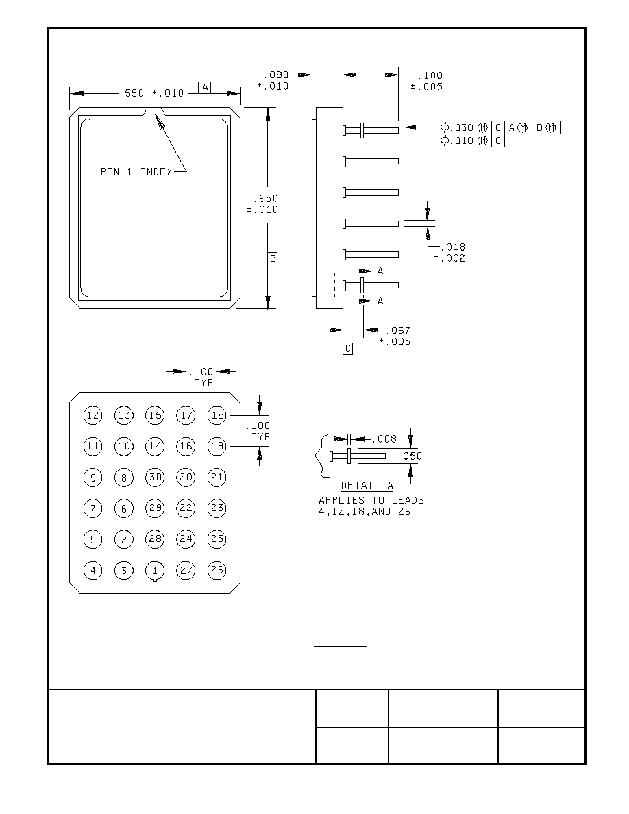
Z
See figure 1
32
Flat package
U
CQCC1-N32
32
Rectangular chip carrier
T
See figure 1
30
Grid array
W
See figure 1
36
Grid array
M
See figure 1
32
Flat package
N
See figure 1
32
Flat package
6
See figure 1(enhanced rad tolerant)
32
Flat package
7
See figure 1(enhanced rad tolerant)
32
Flat package
1.2.5 Lead finish. The lead finish is as specified in MIL-PRF-38535 for device classes Q and V or MIL-PRF-38535, appendix
A for device class M.
1.3 Absolute maximum ratings. 1/ 2/
Supply voltage range (V
) . . . . . . . . . . . . . . . . . . . . . . . . . . . . -0.5 V dc to +6.0 V dc 3/
CC
Operating case temperature range . . . . . . . . . . . . . . . . . . . . . . -55
(
C to +125
(
C
Storage temperature range . . . . . . . . . . . . . . . . . . . . . . . . . . . . -65
(
C to +150
(
C
Lead temperature (soldering, 10 seconds) . . . . . . . . . . . . . . . . +300
(
C
Thermal resistance, junction-to-case (
):
JC
Cases X, Y and U . . . . . . . . . . . . . . . . . . . . . . . . . . . . . . . . . . . See MIL-STD-1835
Cases T and W . . . . . . . . . . . . . . . . . . . . . . . . . . . . . . . . . . . . 21
(
C/W 4/
Case Z . . . . . . . . . . . . . . . . . . . . . . . . . . . . . . . . . . . . . . . . . . . 18
(
C/W 4/
Case M . . . . . . . . . . . . . . . . . . . . . . . . . . . . . . . . . . . . . . . . . . . 3
(
C/W 4/
Case N . . . . . . . . . . . . . . . . . . . . . . . . . . . . . . . . . . . . . . . . . . . 2
(
C/W 4/
Case 6 . . . . . . . . . . . . . . . . . . . . . . . . . . . . . . . . . . . . . . . . . . . 1.5
(
C/W 4/
Case 7 . . . . . . . . . . . . . . . . . . . . . . . . . . . . . . . . . . . . . . . . . . . 1.5
(
C/W 4/
Maximum power dissipation (P ) . . . . . . . . . . . . . . . . . . . . . . . . 1.0 watts
D
Junction temperature (T ) . . . . . . . . . . . . . . . . . . . . . . . . . . . . . +175
(
C 5/
J
Endurance . . . . . . . . . . . . . . . . . . . . . . . . . . . . . . . . . . . . . . . . . 10,000 cycles/byte (minimum)
Data retention . . . . . . . . . . . . . . . . . . . . . . . . . . . . . . . . . . . . . . . 20 years minimum
1.4 Recommended operating conditions.
Supply voltage range (V
) . . . . . . . . . . . . . . . . . . . . . . . . . . . . 4.5 V dc minimum to 5.5 V dc maximum
CC
Supply voltage (V
) . . . . . . . . . . . . . . . . . . . . . . . . . . . . . . . . . 0.0 V dc
SS
High level input voltage range (V
) . . . . . . . . . . . . . . . . . . . . . . 2.0 V dc to V
+ 1.0 V dc 6/
IH
CC
Low level input voltage range (V ) . . . . . . . . . . . . . . . . . . . . . . -0.1 V dc to 0.8 V dc
IL
Case operating temperature range (T ) . . . . . . . . . . . . . . . . . . -55
(
C to +125
(
C
C
1.5 Digital logic testing for device classes Q and V.
Fault coverage measurement of manufacturing
logic tests (MIL-STD-883, test method 5012) . . . . . . . . . . . . . . 100 percent
1/ Stresses above the absolute maximum rating may cause permanent damage to the device. Extended operation at the
maximum levels may degrade performance and affect reliability.
2/ All voltages referenced to V
(V
= ground), unless otherwise specified.
SS
SS
3/ Negative undershoots to a minimum of -1.0 V are allowed with a maximum of 20 ns pulse width.
4/ When the thermal resistance for this case is specified in MIL-STD-1835, that value shall supersede
the value indicated herein.
5/ Maximum junction temperature shall not be exceeded except for allowable short duration burn-in screening
conditions in accordance with method 5004 of MIL-STD-883.
6/ For device types 16-19 only, V
on R
E
S
shall be V
- 0.5 V min. to V
+ 1.0 V max.
IH
CC
CC

STANDARD
MICROCIRCUIT DRAWING
DEFENSE SUPPLY CENTER COLUMBUS
COLUMBUS, OHIO 43216-5000
SIZE
A
5962-38267
REVISION LEVEL
G
SHEET
4
DSCC FORM 2234
APR 97
2. APPLICABLE DOCUMENTS
2.1 Government specification, standards, and handbooks. The following specification, standards, and handbooks form a part
of this drawing to the extent specified herein. Unless otherwise specified, the issues of these documents are those listed in the
issue of the Department of Defense Index of Specifications and Standards (DoDISS) and supplement thereto, cited in the
solicitation.
SPECIFICATION
DEPARTMENT OF DEFENSE
MIL-PRF-38535 - Integrated Circuits, Manufacturing, General Specification for.
STANDARDS
DEPARTMENT OF DEFENSE
MIL-STD-883
-
Test Method Standard Microcircuits.
MIL-STD-1835 -
Interface Standard for Microcircuit Case Outlines.
HANDBOOKS
DEPARTMENT OF DEFENSE
MIL-HDBK-103 -
List of Standard Microcircuit Drawings.
MIL-HDBK-780 -
Standard Microcircuit Drawings.
(Unless otherwise indicated, copies of the specification, standards, and handbooks are available from the Standardization
Document Order Desk, 700 Robbins Avenue, Building 4D, Philadelphia, PA 19111-5094).
2.2 Non-Government publications. The following documents form a part of this document to the extent specified herein. Unless
otherwise specified, the issues of the documents which are DoD adopted are those listed in the issue of the DODISS cited in the
solicitation. Unless otherwise specified, the issues of documents not listed in the DODISS are the issues of the documents cited
in the solicitation.
AMERICAN SOCIETY FOR TESTING AND MATERIALS (ASTM)
ASTM Standard F1192-88 - Standard Guide for the Measurement of Single Event Phenomena from
Heavy Ion Irradiation of Semiconductor Devices.
(Applications for copies of ASTM publications should be addressed to the American Society for Testing and Materials, 1916
Race Street, Philadelphia, PA 19103).
ELECTRONICS INDUSTRIES ASSOCIATION (EIA)
JEDEC Standard EIA/JESD78 - I/C Latch-up Test.
(Applications for copies should be addressed to the Electronics Industries Association, 2500 Wilson Boulevard, Arlington,
VA 22201).
(Non-Government standards and other publications are normally available from the organizations that prepare or distribute
the documents. These documents also may be available in or through libraries or other informational services).
2.3 Order of precedence. In the event of a conflict between the text of this drawing and the references cited herein, the text of
this drawing shall take precedence. Nothing in this document, however, supersedes applicable laws and regulations unless a
specific exemption has been obtained.

STANDARD
MICROCIRCUIT DRAWING
DEFENSE SUPPLY CENTER COLUMBUS
COLUMBUS, OHIO 43216-5000
SIZE
A
5962-38267
REVISION LEVEL
G
SHEET
5
DSCC FORM 2234
APR 97
3. REQUIREMENTS
3.1 Item requirements. The individual item requirements for device classes Q and V shall be in accordance with MIL-PRF-38535
and as specified herein or as modified in the device manufacturer's Quality Management (QM) plan. The modification in the QM
plan shall not affect the form, fit, or function as described herein. The individual item requirements for device class M shall be in
accordance with MIL-PRF-38535, appendix A for non-JAN class level B devices and as specified herein.
3.2 Design, construction, and physical dimensions. The design, construction, and physical dimensions shall be as specified
in MIL-PRF-38535 and herein for device classes Q and V or MIL-PRF-38535, appendix A and herein for device class M.
3.2.1 Case outline(s). The case outline(s) shall be in accordance with 1.2.4 herein and figure 1.
3.2.2 Terminal connections. The terminal connections shall be as specified on figure 2.
3.2.3 Truth table. The truth table shall be as specified on figure 3.
3.2.3.1 Unprogrammed devices. The truth table for unprogrammed devices for contracts involving no altered item drawing
shall be as specified on figure 3 herein. When required, in screening (see 4.2 herein), or quality conformance inspection groups
A, B, C, or D (see 4.4 herein), the devices shall be programmed by the manufacturer prior to test in a checkerboard or similar
pattern (a minimum of 50 percent of the total number of bits programmed).
3.2.3.2 Programmed devices. The requirements for supplying programmed devices are not part of this document.
3.3 Electrical performance characteristics and postirradiation parameter limits. Unless otherwise specified herein, the electrical
performance characteristics and postirradiation parameter limits are as specified in table I and shall apply over the full case
operating temperature range.
3.4 Electrical test requirements. The electrical test requirements shall be the subgroups specified in table IIA. The electrical
tests for each subgroup are defined in table I.
3.5 Marking. The part shall be marked with the PIN listed in 1.2 herein. In addition, the manufacturer's PIN may also be marked
as listed in MIL-HDBK-103. For packages where marking of the entire SMD PIN number is not feasible due to space limitations,
the manufacturer has the option of not marking the "5962-" on the device. For RHA product using this option, the RHA designator
shall still be marked. Marking for device classes Q and V shall be in accordance with MIL-PRF-38535. Marking for device class
M shall be in accordance with MIL-PRF-38535, appendix A.
3.5.1 Certification/compliance mark. The certification mark for device classes Q and V shall be a "QML" or "Q" as required in
MIL-PRF-38535. The compliance mark for device class M shall be a "C" as required in MIL-PRF-38535, appendix A.
3.6 Certificate of compliance. For device classes Q and V, a certificate of compliance shall be required from a QML-38535
listed manufacturer in order to supply to the requirements of this drawing (see 6.6.1 herein). For device class M, a certificate of
compliance shall be required from a manufacturer in order to be listed as an approved source of supply in MIL-HDBK-103 (see 6.6.2
herein). The certificate of compliance submitted to DSCC-VA prior to listing as an approved source of supply for this drawing shall
affirm that the manufacturer's product meets, for device classes Q and V, the requirements of MIL-PRF-38535 and herein or for
device class M, the requirements of MIL-PRF-38535, appendix A and herein.
3.7 Certificate of conformance. A certificate of conformance as required for device classes Q and V in MIL-PRF-38535 or for
device class M in MIL-PRF-38535, appendix A shall be provided with each lot of microcircuits delivered to this drawing.
3.8 Notification of change for device class M. For device class M, notification to DSCC-VA of change of product (see 6.2 herein)
involving devices acquired to this drawing is required for any change as defined in MIL-PRF-38535, appendix A.

STANDARD
MICROCIRCUIT DRAWING
DEFENSE SUPPLY CENTER COLUMBUS
COLUMBUS, OHIO 43216-5000
SIZE
A
5962-38267
REVISION LEVEL
G
SHEET
6
DSCC FORM 2234
APR 97
3.9 Verification and review for device class M. For device class M, DSCC, DSCC's agent, and the acquiring activity retain the
option to review the manufacturer's facility and applicable required documentation. Offshore documentation shall be made available
onshore at the option of the reviewer.
3.10 Microcircuit group assignment for device class M. Device class M devices covered by this drawing shall be in microcircuit
group number 41 (see MIL-PRF-38535, appendix A).
3.11 Processing of EEPROMs. All testing requirements and quality assurance provisions herein shall be satisfied by the
manufacturer prior to delivery.
3.11.1 Conditions of the supplied devices. Devices will be supplied in an unprogrammed or clear state. No provision will be
made for supplying programmed devices.
3.11.2 Erasure of EEPROMs. When specified, devices shall be erased in accordance with procedures and characteristics
specified in 4.5.1.
3.11.3 Programming of EEPROMs. When specified, devices shall be programmed in accordance with procedures and
characteristics specified in 4.5.2.
3.11.4 Verification of state of EEPROMs. When specified, devices shall be verified as either written to the specified pattern
or cleared. As a minimum, verification shall consist of performing a read of the entire array to verify that all bits are in the proper
state. Any bit that does not verify to be in the proper state shall constitute a device failure and the device shall be removed from
the lot or sample.
3.11.5 Power supply sequence of EEPROMs. In order to reduce the probability of inadvertant writes, the following power
supply sequences shall be observed.
a. For device types 1-19, a logic high state shall be applied to W
E
and/or C
E
at the same time or before the application
of V
. For device types 16-19, an additional precaution is available, a logic low state shall be applied to R
E
S
at the
CC
same time or before the application of V
.
CC
b. For device types 1-19, a logic high state shall be applied to W
E
and/or C
E
at the same time or before the removal of
V
. For device types 16-19, an additional precaution is available, a logic low state shall be applied to R
E
S
at the
CC
same time or before the removal of V
.
CC
3.12 Endurance. A reprogrammability test shall be completed as part of the vendor's reliability monitors. This
reprogrammability test shall be done for initial characterization and after any design or process changes which may affect the
reprogrammability of the device. The methods and procedures may be vendor specific, but shall guarantee the number of
program/erase endurance cycles listed in section 1.3 herein over the full military temperature range. The vendor's procedure
shall be kept under document control and shall be made available upon request of the acquiring or preparing activity, along with
test data.
3.13 Data retention. A data retention stress test shall be completed as part of the vendor's reliability monitors. This test shall
be done for initial characterization and after any design or process change which may affect data retention. The methods and
procedures may be vendor specific, but shall guarantee the number of years listed in section 1.3 herein over the full military
temperature range. The vendor's procedure shall be kept under document control and shall be made available upon request
of the acquiring or preparing activity, along with test data.

STANDARD
MICROCIRCUIT DRAWING
DEFENSE SUPPLY CENTER COLUMBUS
COLUMBUS, OHIO 43216-5000
SIZE
A
5962-38267
REVISION LEVEL
G
SHEET
7
DSCC FORM 2234
APR 97
4. QUALITY ASSURANCE PROVISIONS
4.1 Sampling and inspection. For device classes Q and V, sampling and inspection procedures shall be in accordance with MIL-
PRF-38535 or as modified in the device manufacturer's Quality Management (QM) plan. The modification in the QM plan shall not
affect the form, fit, or function as described herein. For device class M, sampling and inspection procedures shall be in accordance
with MIL-PRF-38535, appendix A.
4.2 Screening. For device classes Q and V, screening shall be in accordance with MIL-PRF-38535, and shall be conducted on
all devices prior to qualification and technology conformance inspection. For device class M, screening shall be in accordance with
method 5004 of MIL-STD-883, and shall be conducted on all devices prior to quality conformance inspection.
4.2.1 Additional criteria for device class M.
a.
Delete the sequence specified as initial (preburn-in) electrical parameters through interim (postburn-in) electrical
parameters of method 5004 and substitute lines 1 through 6 of table IIA herein.
b.
Prior to burn-in, the devices shall be programmed (see 4.5.2 herein) with a checkerboard pattern or equivalent
(manufacturers at their option may employ an equivalent pattern provided it is a topologically true alternating bit pattern).
The pattern shall be read before and after burn-in. Devices having bits not in the proper state after burn-in shall constitute
a device failure and shall be included in the PDA calculation and shall be removed from the lot.
c.
The test circuit shall be maintained by the manufacturer under document revision level control and shall be made available
to the preparing or acquiring activity upon request. The test circuit shall specify the inputs, outputs, biases, and power
dissipation, as applicable, in accordance with the intent specified in test method 1015.
(1)
Dynamic burn-in (method 1015 of MIL-STD-883, test condition D; for circuit, see 4.2.1c herein).
d.
Interim and final electrical parameters shall be as specified in table IIA herein.
e.
After the completion of all screening, the device shall be erased and verified prior to delivery.
4.2.2 Additional criteria for device classes Q and V.
a.
The burn-in test duration, test condition and test temperature, or approved alternatives shall be as specified in the device
manufacturer's QM plan in accordance with MIL-PRF-38535. The burn-in test circuit shall be maintained under document
revision level control of the device manufacturer's Technology Review Board (TRB) in accordance with MIL-PRF-38535
and shall be made available to the acquiring or preparing activity upon request. The test circuit shall specify the inputs,
outputs, biases, and power dissipation, as applicable, in accordance with the intent specified in test method 1015 of MIL-
STD-883.
b.
Interim and final electrical test parameters shall be as specified in table IIA herein.
c.
Additional screening for device class V beyond the requirements of device class Q shall be as specified in appendix B of
MIL-PRF-38535.
4.3 Qualification inspection for device classes Q and V. Qualification inspection for device classes Q and V shall be in
accordance with MIL-PRF-38535. Inspections to be performed shall be those specified in MIL-PRF-38535 and herein for groups
A, B, C, D, and E inspections (see 4.4.1 through 4.4.4).
4.4 Conformance inspection. Technology conformance inspection for classes Q and V shall be in accordance with MIL-PRF-
38535 including groups A, B, C, D, and E inspections and as specified herein. Quality conformance inspection for device class
M shall be in accordance with MIL-PRF-38535, appendix A and as specified herein. Inspections to be performed for device class
M shall be those specified in method 5005 of MIL-STD-883 and herein for groups A, B, C, D, and E inspections (see 4.4.1 through
4.4.4).

STANDARD
MICROCIRCUIT DRAWING
DEFENSE SUPPLY CENTER COLUMBUS
COLUMBUS, OHIO 43216-5000
SIZE
A
5962-38267
REVISION LEVEL
G
SHEET
8
DSCC FORM 2234
APR 97
TABLE I. Electrical performance characteristics.
|
|
|
|
|
|
Test
|Symbol | Conditions
| Group A
| Device
| Limits
| Unit
|
| -55
(
C
T
+125
(
C
|subgroups | types
|
|
|
C
|
| V
= 0 V; 4.5 V
V
5.5 V
|
|
| Min
| Max
|
SS
CC
|
| unless otherwise specified
|
|
|
|
|
|
|
|
|
|
|
|
High level input current
|I
|V
= 5.5 V, V
= 5.5 V
| 1, 2, 3
| All
| -5
| 5
| �A
IH
CC
IN
|
|
|
|
|
|
|
|
|
|
|
|
|
|
Low level input current
|I
|V
= 5.5 V, V
= 0.1 V
| 1, 2, 3
| All
| -5
| 5
| �A
IL
CC
IN
|
|
|
|
|
|
|
|
| |
|
| 16-19
| -100
| 100
|
|
| | For R
E
S
input
|
|
|
|
|
|
|
|
|
|
|
|
High impedance output
|I
|V
O
E
V
| 1, 2, 3
|
| -10
| 10
|
OZH
IH
CC
leakage current 1/
|
|V
= 5.5 V, V = 5.5 V
|
|
|
|
|
CC
O
|
|
|
| All
|
|
| �A
|
|
|
|
|
|
|
|I
|V
O
E
V
| 1, 2, 3
|
| -10
| 10
|
OZL
IH
CC
|
|V
= 5.5 V, V = 0.0 V
|
|
|
|
|
CC
O
|
|
|
|
|
|
|
|
|
|
|
|
|
|
Output high voltage
|V
|I
= -400 �A, V
= 4.5 V
| 1, 2, 3
| All
| 2.4
|
| V
OH
OH
CC
|
|V
= 2.0 V, V = 0.8 V
|
|
|
|
|
IH
IL
|
|
|
|
|
|
|
|
|
|
|
|
|
|
Output low voltage
|V
|I
= 2.1 mA, V
= 4.5 V
| 1, 2, 3
| All
|
| 0.4
| V
OL
OL
CC
|
|V
= 2.0 V, V = 0.8 V
|
|
|
|
|
IH
IL
|
|
|
|
|
|
|
|
|
|
|
|
|
|
Input high voltage 2/
|V
|V
= 5.5 V
| 1, 2, 3
| 01-15
| 2.0
| 6.0
| V
IH
CC
|
|
|
|
|
|
|
|
|
|
| 16-19
| 2.2
| 6.0
|
|
|
|
|
|
|
|
Input low voltage 2/
|V
|V
= 4.5 V
| 1, 2, 3
| All
| -0.5
| 0.8
| V
IL
CC
|
|
|
|
|
|
|
|
|
|
|
|
|
|
OE high voltage
|V
|
| 1, 2, 3
| 01-15
| 12
| 13
| V
H
|
|
|
|
|
|
|
|
|
|
|
|V
- |V
+ |
CC
CC
R
E
S
high voltage
|
|
|
| 16-19
| 0.5
| 1.0
|
|
|
|
| 01-06,
|
|
|
Operating supply current
|I
|V
= 5.5 V, WE = V
,
| 1, 2, 3
| 08,13,
|
| 80
| mA
CC1
CC
IH
|
|
|
| 16,17
|
|
|
|
|CE = OE = V
|
| 07,18,
|
| 100
|
IL
|
|f = 1/t
min
|
| 19
|
|
|
AVAV
|
|
|
| 09-12,
|
| 120
|
|
|
|
| 14,15
|
|
|
|
|
|
|
|
|
|
Standby supply current
|I
|V
= 5.5 V, CE = V
,
| 1, 2, 3
| All
|
| 3
| mA
CC2
CC
IH
TTL
|
| all I/O's = open,
|
|
|
|
|
|
|OE = V , f = 0 Hz
|
|
|
|
|
IL
|
|
|
|
|
|
|
|
|
|
|
|
|
|
Standby supply current
|I
|V
= 5.5 V, CE = V
-0.3 V
| 1, 2, 3
| 01-07
|
| 850
| �A
CC3
CC
CC
CMOS
|
|Inputs = V
, I/O's = open,
|
| 08-12
|
| 500
|
IH
|
|OE = V , f = 0 Hz
|
| 13-15,
|
| 350
|
IL
|
|
|
| 16-19
|
|
|
See footnotes at end of table.

STANDARD
MICROCIRCUIT DRAWING
DEFENSE SUPPLY CENTER COLUMBUS
COLUMBUS, OHIO 43216-5000
SIZE
A
5962-38267
REVISION LEVEL
G
SHEET
9
DSCC FORM 2234
APR 97
TABLE I. Electrical performance characteristics - Continued.
|
|
|
|
|
|
Test
|Symbol | Conditions
| Group A
| Device
| Limits
| Unit
|
| -55
(
C
T
+125
(
C
|subgroups | types
|
|
|
C
|
| V
= 0 V; 4.5 V
V
5.5 V
|
|
| Min
| Max
|
SS
CC
|
| unless otherwise specified
|
|
|
|
|
|
|
|
|
|
|
|
Input capacitance 3/ 4/
|C
|V
= 0 V, f = 1.0 MHz,
| 4
| All
|
| 10.0 | pF
IN
IN
|
|T = +25
(
C, see 4.4.1c
|
|
|
|
|
C
|
|
|
|
|
|
|
|
|
|
|
|
|
|
Output capacitance 3/ 4/
|C
|V
= 0 V, f = 1.0 MHz
| 4
| All
|
| 12.0 | pF
OUT
OUT
|
|T = +25
(
C, see 4.4.1c
|
|
|
|
|
C
|
|
|
|
|
|
|
|
|
|
|
|
|
|
Functional tests
|
| See 4.4.1d
| 7,8A,8B
| All
|
|
|
|
|
|
|
|
|
|
|
|
|
|
|
|
|
|
| See figures 4, 5, and 6 as
|
|01-02,16 | 250
|
|
|
| applicable. 5/
|
|03-04,17 | 200
|
|
|
|
|
|05-06,18 | 150
|
|
Read cycle time
|t
|
|9, 10, 11
| 07,08,
| 120
|
| ns
AVAV
|
|
|
| 13,19
|
|
|
|
|
|
| 09,10,
| 90
|
|
|
|
|
| 14
|
|
|
|
|
|
| 11,12,
| 70
|
|
|
|
|
| 15
|
|
|
|
|
|
|
|
|
|
|
|
|
|01-02,16 |
| 250
|
|
|
|
|03-04,17 |
| 200
|
Address access time
|t
|
|9, 10, 11
|05-06,18 |
| 150
|
AVQV
|
|
|
| 07,08,
|
| 120
| ns
|
|
|
| 13,19
|
|
|
|
|
|
| 09,10,
|
| 90
|
|
|
|
| 14
|
|
|
|
|
|
| 11,12,
|
| 70
|
|
|
|
| 15
|
|
|
|
|
|
|
|
|
|
|
|
|
|01-02,16 |
| 250
|
|
|
|
|03-04,17 |
| 200
|
CE access time
|t
|
|9, 10, 11
|05-06,18 |
| 150
|
ELQV
|
|
|
| 07,08,
|
| 120
| ns
|
|
|
| 13,19
|
|
|
|
|
|
| 09,10,
|
| 90
|
|
|
|
| 14
|
|
|
|
|
|
| 11,12,
|
| 70
|
|
|
|
| 15
|
|
|
|
|
|
|
|
|
|
OE access time
|t
|
|9, 10, 11
| 01-06
|
| 55
| ns
OLQV
|
|
|
| 07-15
|
| 50
|
|
|
|
| 16-19
|
| 75
|
|
|
|
|
|
|
|
CE to output in low Z
|t
|
|9, 10, 11
| All
| 0
|
| ns
ELQX
4/
|
|
|
|
|
|
|
|
|
|
|
|
|
|
|
|
|
|
|
|
|
Chip disable to output
|t
|
|9, 10, 11
| 01-06
|
| 55
| ns
EHQZ
in high Z 4/
|
|
|
| 07-19
|
| 50
|
|
|
|
|
|
|
|
See footnotes at end of table.

STANDARD
MICROCIRCUIT DRAWING
DEFENSE SUPPLY CENTER COLUMBUS
COLUMBUS, OHIO 43216-5000
SIZE
A
5962-38267
REVISION LEVEL
G
SHEET
10
DSCC FORM 2234
APR 97
TABLE I. Electrical performance characteristics - Continued.
|
|
|
|
|
|
Test
|Symbol
| Conditions
| Group A
| Device
| Limits
| Unit
|
| -55
(
C
T
+125
(
C
|subgroups | types
|
|
|
C
|
| V
= 0 V; 4.5 V
V
5.5 V
|
|
| Min
| Max
|
SS
CC
|
| unless otherwise specified
|
|
|
|
|
|
|
|
|
|
|
|
OE to output in low Z
|t
|See figures 4, 5, and 6 as
|9, 10, 11
| All
| 0
|
| ns
OLQX
4/
|
| applicable. 5/
|
|
|
|
|
|
|
|
|
|
|
|
|
|
|
|
|
|
|
Output disable to output
|t
|
|9, 10, 11
| 01-06
|
| 55
| ns
OHQZ
in high Z 4/
|
|
|
| 07-19
|
| 50
|
|
|
|
|
|
|
|
|
|
|
|
|
|
|
Output hold from address
|t
|
|9, 10, 11
| All
| 0
|
| ns
AXQX
change
|
|
|
|
|
|
|
|
|
|
|
|
|
|
|
|
|
| 01,03,
|
|
|
|
|
|
| 05,07,
|
|
|
|
|
|9, 10, 11
| 09,11,
|
| 10
|
Write cycle time
|t
|
|
| 16-19
|
|
| ms
WHWL1
|t
|
|
| 02,04
|
|
|
EHEL1
|
|
|
| 06
|
| 5
|
|
|
|
| 08,10,
|
| 3
|
|
|
|
| 12-15
|
|
|
|
|
|
|
|
|
|
Address setup time
|t
|
|9, 10, 11
| All
| 0
|
| ns
AVWL
|t
|
|
|
|
|
|
AVEL
|
|
|
|
|
|
|
|
|
|
| 16-19
| 150
|
|
Address hold time
|t
|
|9, 10, 11
| 01-08,
| 70
|
| ns
WLAX
|t
|
|
| 13
|
|
|
ELAX
|
|
|
| 09-12,
|
|
|
|
|
|
| 14,15
| 50
|
|
|
|
|
|
|
|
|
Write setup time
|t
|
|9, 10, 11
| All
| 0
|
| ns
ELWL
|t
|
|
|
|
|
|
WLEL
|
|
|
|
|
|
|
|
|
|
|
|
|
|
Write hold time
|t
|
|9, 10, 11
| All
| 0
|
| ns
WHEH
|t
|
|
|
|
|
|
EHWH
|
|
|
|
|
|
|
|
|
|
|
|
|
|
OE setup time
|t
|
|9, 10, 11
| 01-15
| 10
|
| ns
OHWL
|t
|
|
|
|
|
|
OHEL
|
|
|
| 16-19
| 0
|
|
|
|
|
|
|
|
|
OE hold time
|t
|
|9, 10, 11
| 01-15
| 10
|
| ns
WHOL
|t
|
|
|
|
|
|
EHOL
|
|
|
| 16-19
| 0
|
|
|
|
|
|
|
|
|
Write pulse width (page
|t
|
|9, 10, 11
| 01-15
| 100 |
| ns
WLWH
or byte write)
|t
|
|
|
|
|
|
ELEH
|
|
|
| 16-19
| 250
|
|
|
|
|
| 16-19
| 100
|
|
Data setup time
|t
|
|9, 10, 11
| 01-08,
| 60
|
| ns
DVWH
|t
|
|
| 13
|
|
|
DVEH
|
|
|
| 09-12,
| 40
|
|
|
|
|
| 14,15
|
|
|
See footnotes at end of table.

STANDARD
MICROCIRCUIT DRAWING
DEFENSE SUPPLY CENTER COLUMBUS
COLUMBUS, OHIO 43216-5000
SIZE
A
5962-38267
REVISION LEVEL
G
SHEET
11
DSCC FORM 2234
APR 97
TABLE I. Electrical performance characteristics - Continued.
|
|
|
|
|
|
Test
|Symbol
| Conditions
| Group A
| Device
| Limits
| Unit
|
| -55
(
C
T
+125
(
C
|subgroups | types
|
|
|
C
|
| V
= 0 V; 4.5 V
V
5.5 V
|
|
| Min
| Max
|
SS
CC
|
| unless otherwise specified
|
|
|
|
|
|
|
|
| 01-07
|
|
|
Data hold time
|t
|See figures 4, 5, and 6 as
|9, 10, 11
| 16-19
| 10
|
| ns
WHDX
|t
| applicable. 5/
|
| 08-15
| 0
|
|
EHDX
|
|
|
|
|
|
|
|
|
|
|
|
|
|
Byte load cycle
|t
|
|9, 10, 11
| 01-15
| .20
| 149
| �s
WHWL2
|
|
|
|
|
|
|
|
|
|
| 16-19
| .3
| 30
|
|
|
|
|
|
|
|
|
|
|
|01-02,16 |
| 250
|
|
|
|
|03-04,17 |
| 200
|
Last byte loaded to data
|t
|
|9, 10, 11
|05-06,18 |
| 150
|
WHEL
polling
|t
|
|
|07,08,
|
| 120
| ns
EHEL
|
|
|
|13,19
|
|
|
|
|
|
|09,10,
|
| 90
|
|
|
|
|14
|
|
|
|
|
|
|11,12,
|
| 70
|
|
|
|
|15
|
|
|
|
|
|
|
|
|
|
CE setup time
|t
|See figures 4, 5, and 6 as
|9, 10, 11
| 01-15
| 5
|
| �s
ELWL
(chip erase)
|
| applicable. 5/ 6/
|
|
|
|
|
|
|
|
|
|
|
|
|
|
|
|
|
|
|
OE setup time
|t
|
|9, 10, 11
| 01-15
| 5
|
| �s
OVHWL
(chip erase)
|
|
|
|
|
|
|
|
|
|
|
|
|
|
|
|
|
| 01-07
| 10
|
| ms
WE pulse width (chip
|t
|
|9, 10, 11
|
|
|
|
WLWH2
erase)
|
|
|
| 08-15
| 10
|
| �s
|
|
|
|
|
|
|
|
|
|
|
|
|
|
CE hold time
|t
|
|9, 10, 11
| 01-15
| 5
|
| �s
WHEH
(chip erase)
|
|
|
|
|
|
|
|
|
|
|
|
|
|
|
|
|
|
|
|
|
OE hold time (chip erase)
|t
|
|9, 10, 11
| 01-15
| 5
|
| �s
WHOH
|
|
|
|
|
|
|
|
|
|
|
|
|
|
High voltage
|V
|
|9, 10, 11
| 01-15
| 12
| 13
| V
H
(chip erase)
|
|
|
|
|
|
|
|
|
|
|
|
|
|
|
|
|
|
|
|
|
Clear recovery
|t
|
|9, 10, 11
| 01-15
|
| 50
| ms
OLEL
(chip erase)
|
|
|
|
|
|
|
|
|
|
|
|
|
|
|
|
|
|
|
|
|
Data setup time
|t
|
|9, 10, 11
| 01-15
| 1
|
| �s
DHWL
(chip erase) 7/
|
|
|
|
|
|
|
|
|
|
|
|
|
|
|
|
|
|
|
|
|
Data hold time during
|t
|
|9, 10, 11
| 01-15
| 1
|
| �s
WHDX
chip erase cycle 7/
|
|
|
|
|
|
|
|
|
|
|
|
|
|
See footnotes at end of table.

STANDARD
MICROCIRCUIT DRAWING
DEFENSE SUPPLY CENTER COLUMBUS
COLUMBUS, OHIO 43216-5000
SIZE
A
5962-38267
REVISION LEVEL
G
SHEET
12
DSCC FORM 2234
APR 97
TABLE I. Electrical performance characteristics - Continued.
|
|
|
|
|
|
Test
|Symbol
| Conditions
| Group A
| Device
| Limits
| Unit
|
| -55
(
C
T
+125
(
C
|subgroups | types
|
|
|
C
|
| V
= 0 V; 4.5 V
V
5.5 V
|
|
| Min
| Max
|
SS
CC
|
| unless otherwise specified
|
|
|
|
|
|
|
|
|
|
|
|
R
E
S
low to output float
|t
|See figures 4, 5, and 6 as
|9, 10, 11
| 16-19
| 0
| 350
| ns
DFR
|
| applicable. 5/ 8/
|
|
|
|
|
|
|
|
|
|
|
|
|
|
|
|
|
|
|
R
E
S
to output delay
|t
|
|9, 10, 11
| 16-19
| 0
| 450
| ns
RR
|
|
|
|
|
|
|
|
|
|
|
|
|
|
Reset protect time
|t
|
|9, 10, 11
| 16-19
| 100
|
| �s
RP
|
|
|
|
|
|
|
|
|
|
|
|
|
|
Reset high time
|t
|
|9, 10, 11
| 16-19
| 1.0
|
| �s
RES
|
|
|
|
|
|
|
|
|
|
|
|
|
|
Time to device busy
|t
|
|9, 10, 11
| 16-19
| 120
|
| ns
DB
|
|
|
|
|
|
|
1/ Connect all address inputs and O
E
to V
and measure I
and I
with the output under test connected to V
.
IH
OZL
OZH
OUT
Terminal conditions for the output leakage current test shall be as follows:
a.
V
= 2.0 V for device types 01-15 and 2.2 V for device types 16-19; V = 0.8 V.
IH
IL
b.
For I
: Select an appropriate address to acquire a logic "1" on the designated output. Apply V
to C
E
.
OZL
IH
Measure the leakage current while applying the specified voltage.
c.
For I
: Select an appropriate address to acquire a logic "0" on the designated output. Apply V
to C
E
.
OZH
IH
Measure the leakage current while applying the specified voltage.
2/ A functional test shall verify the dc input and output levels and applicable patterns as appropriate, all input
and I/O pins shall be tested. Terminal conditions are as follows:
a.
Inputs: H =2.0 V for device types 01-15 and 2.2 V for device types 16-19; L = 0.8 V. Outputs: H = 2.4 V minimum and
L = 0.4 V maximum.
b.
The functional tests shall be performed with V
= 4.5 and V
= 5.5 V.
CC
CC
3/ All pins not being tested are to be open.
4/ Tested initially and after any design or process changes which may affect that parameter, and therefore shall be
guaranteed to the limits specified in table I.
5/ Tested by application of specified timing signals and conditions.
Equivalent ac test conditions:
Output load, see figure 5; input rise and fall times
10 ns; input pulse levels, 0.4 V and 2.4 V; timing measurement
reference levels, inputs, 1.5 V for device types 1-15 and 1 V and 2 V for device types 16-19; outputs, 1.5 V for device types
1-15 and 0.8 V and 2 V for device types 16-19.
6/ Chip erase functions are applicable to device types 01-15 only.
7/ This parameter not applicable for internal timer controlled devices.
8/ R
E
S
functions are applicable to device types 16-19 only.

STANDARD
MICROCIRCUIT DRAWING
DEFENSE SUPPLY CENTER COLUMBUS
COLUMBUS, OHIO 43216-5000
SIZE
A
5962-38267
REVISION LEVEL
G
SHEET
13
DSCC FORM 2234
APR 97
4.4.1 Group A inspection.
a.
Tests shall be as specified in table IIA herein.
b.
Subgroups 5 and 6 in table I, method 5005 of MIL-STD-883 shall be omitted.
c.
Subgroup 4 (C
and C
measurements) shall be measured only for initial qualification and after any process or design
IN
OUT
changes which may affect input or output capacitance. Capacitance shall be measured between the designated terminal
and GND at a frequency of 1 MHz. Sample size is 15 devices with no failures and all input and output terminals tested.
d.
For device class M, subgroups 7 and 8 tests shall be sufficient to verify the truth table. For device classes Q and V,
subgroups 7 and 8 shall include verifying the functionality of the device, these tests shall have been fault graded in
accordance with MIL-STD-883, test method 5012 (see 1.5 herein).
e.
O/V (latch-up) tests shall be measured only for initial qualification and after any design or process changes which may
affect the performance of the device. For device class M, procedures and circuits shall be maintained under document
revision level control by the manufacturer and shall be made available to the preparing activity or acquiring activity upon
request. For device classes Q and V, the procedures and circuits shall be under the control of the device manufacturer's
TRB in accordance with MIL-PRF-38535 and shall be made available to the preparing activity or acquiring activity upon
request. Testing shall be on all pins, on five devices with zero failures. Latch-up test shall be considered destructive.
Information contained in JEDEC Standard EIA/JESD78 may be used for reference.
f. All devices selected for testing shall be programmed with a checkerboard pattern or equivalent. After completion of all
testing, the devices shall be erased and verified, (except devices submitted for groups C and D testing).
4.4.2 Group C inspection. The group C inspection end-point electrical parameters shall be as specified in table IIA herein.
4.4.2.1 Additional criteria for device class M.
a. Steady-state life test conditions, method 1005 of MIL-STD-883:
(1)
The device selected for testing shall be programmed with a checkerboard pattern. After completion of all testing, the
devices shall be erased and verified (except devices submitted for group D testing).
(2)
Test condition D or E. The test circuit shall be maintained by the manufacturer under document revision level control
and shall be made available to the preparing or acquiring activity upon request. The test circuit shall specify the inputs,
outputs, biases, and power dissipation, as applicable, in accordance with the intent specified in test method 1005.
(3)
T = +125
(
C, minimum.
A
(4)
Test duration: 1,000 hours, except as specified in method 1005 of MIL-STD-883.
b.
All devices requiring end-point electrical testing shall be programmed with a checkerboard or equivalent alternating bit
pattern.
c.
After the completion of all testing, the devices shall be cleared and verified prior to delivery.
4.4.2.2 Additional criteria for device classes Q and V. The steady-state life test duration, test condition and test temperature,
or approved alternatives shall be as specified in the device manufacturer's QM plan in accordance with MIL-PRF-38535. The test
circuit shall be maintained under document revision level control by the device manufacturer's TRB, in accordance with MIL-
PRF-38535, and shall be made available to the acquiring or preparing activity upon request. The test circuit shall specify the inputs,
outputs, biases, and power dissipation, as applicable, in accordance with the intent specified in test method 1005 of MIL-STD-883.
4.4.3 Group D inspection. The group D inspection end-point electrical parameters shall be as specified in table IIA herein. The
devices selected for testing shall be programmed with a checkerboard pattern. After completion of all testing, the devices shall be
erased and verified.

STANDARD
MICROCIRCUIT DRAWING
DEFENSE SUPPLY CENTER COLUMBUS
COLUMBUS, OHIO 43216-5000
SIZE
A
5962-38267
REVISION LEVEL
G
SHEET
14
DSCC FORM 2234
APR 97
Case T
FIGURE 1. Case outline.

STANDARD
MICROCIRCUIT DRAWING
DEFENSE SUPPLY CENTER COLUMBUS
COLUMBUS, OHIO 43216-5000
SIZE
A
5962-38267
REVISION LEVEL
G
SHEET
15
DSCC FORM 2234
APR 97
Case W
FIGURE 1. Case outline - Continued.

STANDARD
MICROCIRCUIT DRAWING
DEFENSE SUPPLY CENTER COLUMBUS
COLUMBUS, OHIO 43216-5000
SIZE
A
5962-38267
REVISION LEVEL
G
SHEET
16
DSCC FORM 2234
APR 97
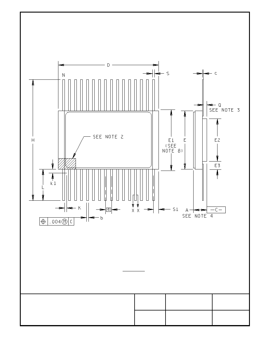
Case Z
FIGURE 1. Case outline - Continued.

STANDARD
MICROCIRCUIT DRAWING
DEFENSE SUPPLY CENTER COLUMBUS
COLUMBUS, OHIO 43216-5000
SIZE
A
5962-38267
REVISION LEVEL
G
SHEET
17
DSCC FORM 2234
APR 97
Case Z
Variations (all dimensions shown in inches)
Symbol
Min
Max
Notes
A
b
b1
C
C1
D
E
E1
E2
E3
.090
.015
.015
.004
.004
.430
.330
.030
.120
.020
.019
.007
.006
.830
.488
.498
4
8
e
.050 BSC
H
k
.008
1.228
.015
2, 5
k1
.025 ref
2, 5
L
Q
S
S1
.270
.026
.005
.370
.045
.045
3
N
32
6
Inches mm | Inches mm
| Inches mm
.004 0.10 | .020 0.51 | .270 6.86
.005 0.13 | .025 0.64
| .350 8.89
.006 0.15 | .026 0.66
| .370 9.40
.007 0.18 | .030 0.76
| .472 11.99
.008 0.20 | .045 1.14
| .488 12.40
.015 0.38 | .050 1.27
| .498 12.65
.019 0.48 | .120 3.05
| 1.228 31.19
NOTES:
1.
All dimensions and tolerances conform to ANSI Y14.5M-1982.
2.
Index area: An identification mark shall be located adjacent to pin 1 within the shaded area shown. Alternatively,
a tab (dim k) may be used as shown.
3.
Dimension Q shall be measured from the point on the lead located opposite the braze pad.
4.
This dimension includes lid thickness.
5.
Optional, see note 2. If pin 1 identification is used instead of this tab, the minimum dimension does not apply.
6.
(N) indicates number of leads.
7.
Uses a metal lid.
8.
Includes braze fillet.
9.
Metric equivalents are given for general information only.
FIGURE 1. Case outline - Continued.

STANDARD
MICROCIRCUIT DRAWING
DEFENSE SUPPLY CENTER COLUMBUS
COLUMBUS, OHIO 43216-5000
SIZE
A
5962-38267
REVISION LEVEL
G
SHEET
18
DSCC FORM 2234
APR 97
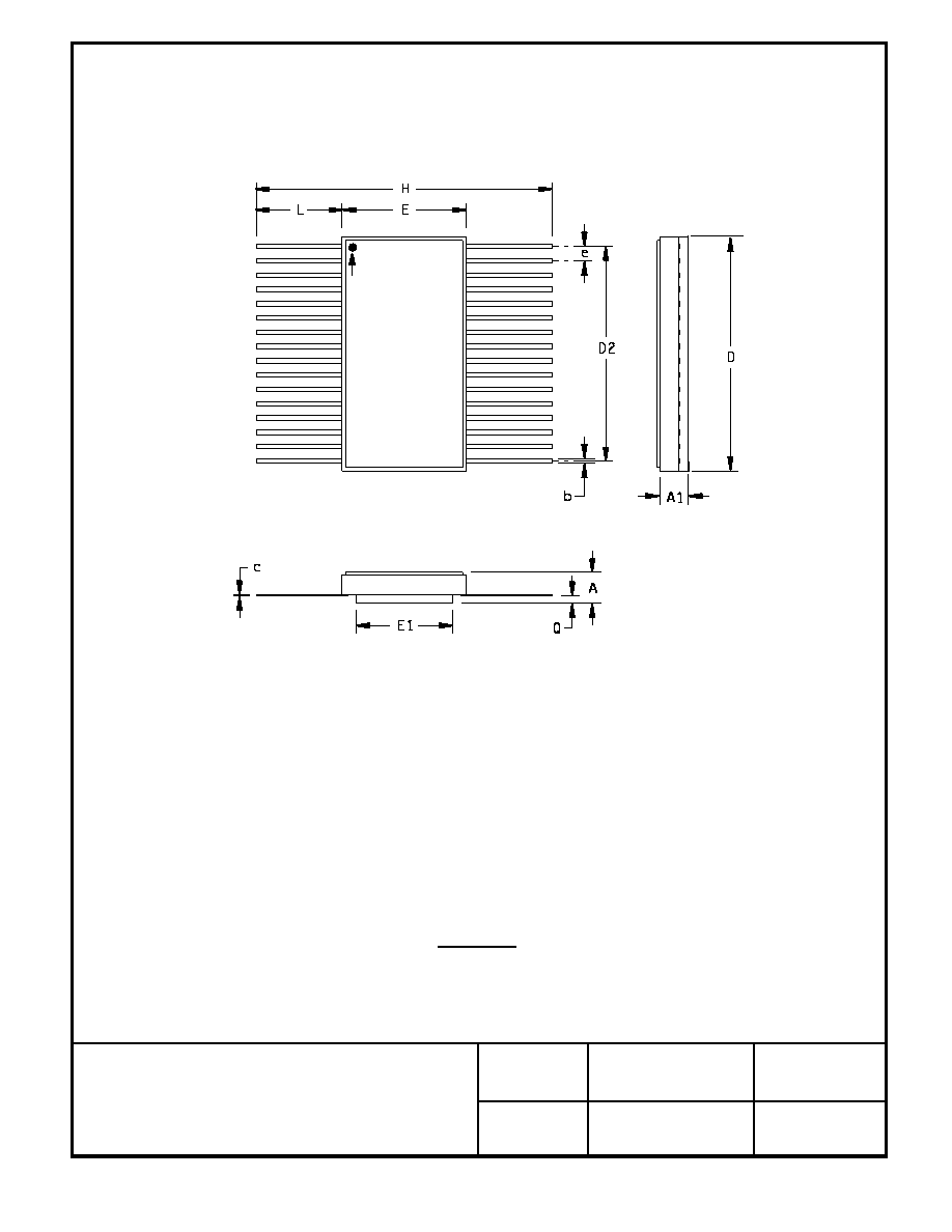
Case M
Pin 1 indicator
FIGURE 1. Case outline - Continued.

STANDARD
MICROCIRCUIT DRAWING
DEFENSE SUPPLY CENTER COLUMBUS
COLUMBUS, OHIO 43216-5000
SIZE
A
5962-38267
REVISION LEVEL
G
SHEET
19
DSCC FORM 2234
APR 97
Case M
Variations
Symbol
Millimeters
Inches
Min
Max
Min
Max
A
A1
b
c
D
D2
E
E1
2.46
2.29
.038
0.08
20.57
18.92
10.80
8.38
3.12
2.79
.048
0.18
21.08
19.18
11.30
9.04
.097
.090
.015
.003
.810
.745
.425
.330
.123
.110
.019
.007
.830
.755
.445
.356
e
1.14
1.40
.045
.055
H
25.40
27.94
1.00
1.10
L
Q
7.37
0.66
7.87
0.94
.290
.026
.310
.037
N
32
NOTE:
Although dimensions are in inches, the US government preferred system of measurement is the metric SI system.
However, since this item was originally designed using inch-pound units of measurement, in the event of conflict
between the two, the inch-pound units shall take precedence. Metric equivalents are for general information only.
FIGURE 1. Case outline - Continued.

STANDARD
MICROCIRCUIT DRAWING
DEFENSE SUPPLY CENTER COLUMBUS
COLUMBUS, OHIO 43216-5000
SIZE
A
5962-38267
REVISION LEVEL
G
SHEET
20
DSCC FORM 2234
APR 97
Case N
Pin 1 indicator
FIGURE 1. Case outline - Continued.

STANDARD
MICROCIRCUIT DRAWING
DEFENSE SUPPLY CENTER COLUMBUS
COLUMBUS, OHIO 43216-5000
SIZE
A
5962-38267
REVISION LEVEL
G
SHEET
21
DSCC FORM 2234
APR 97
Case N
Variations
Symbol
Millimeters
Inches
Min
Max
Min
Max
A
A1
b
c
D
D1
D2
E
E1
3.18
2.29
0.38
0.08
20.57
19.69
18.92
10.80
7.37
3.81
2.79
0.48
0.18
21.08
19.94
19.18
11.30
7.87
.125
.090
.015
.003
.810
.775
.745
.425
.290
.150
.110
.019
.007
.830
.785
.755
.445
.310
e
1.14
1.40
.045
.055
H
25.40
27.94
1.00
1.10
L
Q
7.37
0.66
7.87
0.94
.290
.026
.310
.037
N
32
NOTE:
Although dimensions are in inches, the US government preferred system of measurement is the metric SI system.
However, since this item was originally designed using inch-pound units of measurement, in the event of conflict
between the two, the inch-pound units shall take precedence. Metric equivalents are for general information only.
FIGURE 1. Case outline - Continued.

STANDARD
MICROCIRCUIT DRAWING
DEFENSE SUPPLY CENTER COLUMBUS
COLUMBUS, OHIO 43216-5000
SIZE
A
5962-38267
REVISION LEVEL
G
SHEET
22
DSCC FORM 2234
APR 97
Case 6
FIGURE 1. Case outline - Continued.

STANDARD
MICROCIRCUIT DRAWING
DEFENSE SUPPLY CENTER COLUMBUS
COLUMBUS, OHIO 43216-5000
SIZE
A
5962-38267
REVISION LEVEL
G
SHEET
23
DSCC FORM 2234
APR 97
Case 6
Variations
Symbol
Millimeters
Inches
Min
Max
Min
Max
A
b
c
D
E
E1
E2
E3
3.07
0.38
0.10
11.99
7.72
0.76
3.81
0.56
0.18
21.08
12.40
7.87
.121
.015
.004
.472
.304
.030
.150
.022
.009
.830
.488
.498
e
1.27
.050 BSC
S1
0.13
.005
L
Q
7.37
0.51
7.87
1.14
.355
.020
.375
.045
N
32
NOTE:
Although dimensions are in inches, the US government preferred system of measurement is the metric SI system.
However, since this item was originally designed using inch-pound units of measurement, in the event of conflict
between the two, the inch-pound units shall take precedence. Metric equivalents are for general information only.
This package is manufactured for additonal Rad tolerant capabilities, contact the vendor for specific information.
FIGURE 1. Case outline - Continued.

STANDARD
MICROCIRCUIT DRAWING
DEFENSE SUPPLY CENTER COLUMBUS
COLUMBUS, OHIO 43216-5000
SIZE
A
5962-38267
REVISION LEVEL
G
SHEET
24
DSCC FORM 2234
APR 97
Case 7
FIGURE 1. Case outline - Continued.

STANDARD
MICROCIRCUIT DRAWING
DEFENSE SUPPLY CENTER COLUMBUS
COLUMBUS, OHIO 43216-5000
SIZE
A
5962-38267
REVISION LEVEL
G
SHEET
25
DSCC FORM 2234
APR 97
Case 7
Variations
Symbol
Millimeters
Inches
Min
Max
Min
Max
A
b
c
D
E
E1
E2
E3
3.18
.038
0.08
10.26
5.94
0.76
3.81
0.56
0.23
21.08
10.57
11.18
.117
.015
.003
.404
.234
.030
.143
.022
.009
.830
.416
.440
e
1.27
.050 BSC
S1
0.13
.005
L
Q
8.89
0.53
10.41
0.91
.350
.021
.410
.036
N
32
NOTE:
Although dimensions are in inches, the US government preferred system of measurement is the metric SI system.
However, since this item was originally designed using inch-pound units of measurement, in the event of conflict
between the two, the inch-pound units shall take precedence. Metric equivalents are for general information only.
This package is manufactured for additonal Rad tolerant capabilities, contact the vendor for specific information.
FIGURE 1. Case outline - Continued.

STANDARD
MICROCIRCUIT DRAWING
DEFENSE SUPPLY CENTER COLUMBUS
COLUMBUS, OHIO 43216-5000
SIZE
A
5962-38267
REVISION LEVEL
G
SHEET
26
DSCC FORM 2234
APR 97
Device types
01 - 15
16 - 19
Case outlines
X, Z, U
Y
W
T
U
M, N,6,7
Terminal number
Terminal symbol
1
2
3
4
5
6
7
8
9
10
11
12
13
14
15
16
17
18
19
20
21
22
23
24
25
26
27
28
29
30
31
32
33
34
35
36
37
38
39
40
41
42
43
44
NC
A16
A15
A12
A7
A6
A5
A4
A3
A2
A1
A0
I/O0
I/O1
I/O2
VSS
I/O3
I/O4
I/O5
I/O6
I/O7
C
E
A10
O
E
A11
A9
A8
A13
A14
NC
W
E
VCC
---
---
---
---
---
---
---
---
---
---
---
---
NC
NC
NC
NC
A16
A15
A12
A7
A6
A5
NC
NC
NC
A4
A3
A2
A1
A0
I/O0
I/O1
I/O2
VSS
NC
I/O3
I/O4
I/O5
I/O6
I/O7
C
E
A10
O
E
NC
NC
NC
NC
A11
A9
A8
A13
A14
NC
NC
W
E
VCC
NC
NC
NC
A16
A15
A12
A7
A6
A5
A4
A3
A2
A1
A0
I/O0
I/O1
I/O2
VSS
I/O3
I/O4
I/O5
I/O6
I/O7
C
E
A10
O
E
A11
A9
A8
A13
A14
NC
NC
NC
W
E
VCC
---
---
---
---
---
---
---
---
A14
A12
A7
A6
A5
A4
A3
A2
A1
A0
I/O0
I/O1
I/O2
VSS
I/O3
I/O4
I/O5
I/O6
I/O7
C
E
A10
O
E
A11
A9
A8
A13
W
E
VCC
A15
A16
---
---
---
---
---
---
---
---
---
---
---
---
---
---
RDY/B
U
S
Y
A16
A14
A12
A7
A6
A5
A4
A3
A2
A1
A0
I/O0
I/O1
I/O2
VSS
I/O3
I/O4
I/O5
I/O6
I/O7
C
E
A10
O
E
A11
A9
A8
A13
W
E
R
E
S
A15
VCC
---
---
---
---
---
---
---
---
---
---
---
---
RDY/B
U
S
Y
A16
A14
A12
A7
A6
A5
A4
A3
A2
A1
A0
I/O0
I/O1
I/O2
VSS
I/O3
I/O4
I/O5
I/O6
I/O7
C
E
A10
O
E
A11
A9
A8
A13
W
E
R
E
S
A15
VCC
---
---
---
---
---
---
---
---
---
---
---
---
NC = no connection
FIGURE 2. Terminal connections.

STANDARD
MICROCIRCUIT DRAWING
DEFENSE SUPPLY CENTER COLUMBUS
COLUMBUS, OHIO 43216-5000
SIZE
A
5962-38267
REVISION LEVEL
G
SHEET
27
DSCC FORM 2234
APR 97
Device types 01-15
Mode
C
E
O
E
W
E
I/O
Read
VIL
VIL
VIH
DOUT
Write
VIL
VIH
VIL
DIN
Standby
VIH
X
X
High Z
Write inhibit
X
X
VIH D
or High Z
OUT
Write inhibit
VIH
X
X
High Z
Write inhibit
X
VIL
X
D
or High Z
OUT
Write inhibit
VIL
VIL
VIL
No operation
Software chip clear
VIL
VIH
VIL
DIN
Software write protect
VIL
VIH
VIL
DIN
High voltage chip clear
VIL
VH
VIL
VIH
V
= High logic, "1" state, V = Low logic, "0" state.
IH
IL
X = logic "don't care" state, High Z = high impedance state.
V = Chip clear voltage, D
= Data out, and
H
OUT
D
= Data in.
IN
Device types 16-19
Mode
C
E
O
E
W
E
R
E
S
RDY/B
U
S
Y
I/O
Read
VIL
VIL
VIH
VH
High Z
DOUT
Standby
VIH
X
X
X
High Z
High Z
Write
VIL
VIH
VIL
VH
High Z to VOL
DIN
Deselect
VIL
VIH
VIH
VH
High Z
High Z
Write inhibit
X
X
VIH
X
---
---
Write inhibit
X
VIL
X
X
---
---
D
A
T
A
polling
VIL
VIL
VIH
VH
VOL
D
(I/O7)
OUT
Program reset
X
X
X
VIL
High Z
High Z
V
= High logic, "1" state, V = Low logic, "0" state.
IH
IL
X = logic "don't care" state, High Z = high impedance state.
D
= Data in, D
= Data out, and V = V
-0.5 V to V
+1.0 V.
IN
OUT
H
CC
CC
.
FIGURE 3. Truth table.

STANDARD
MICROCIRCUIT DRAWING
DEFENSE SUPPLY CENTER COLUMBUS
COLUMBUS, OHIO 43216-5000
SIZE
A
5962-38267
REVISION LEVEL
G
SHEET
28
DSCC FORM 2234
APR 97
READ MODE WAVEFORM
NOTE: R
E
S
waveform is applicable to device types 16-19 only.
FIGURE 4. Waveforms.

STANDARD
MICROCIRCUIT DRAWING
DEFENSE SUPPLY CENTER COLUMBUS
COLUMBUS, OHIO 43216-5000
SIZE
A
5962-38267
REVISION LEVEL
G
SHEET
29
DSCC FORM 2234
APR 97
WE CONTROLLED BYTE WRITE WAVEFORMS
NOTE: RDY/B
U
S
Y
, R
E
S
, and V
waveforms are applicable to device types 16-19 only.
CC
FIGURE 4. Waveforms.

STANDARD
MICROCIRCUIT DRAWING
DEFENSE SUPPLY CENTER COLUMBUS
COLUMBUS, OHIO 43216-5000
SIZE
A
5962-38267
REVISION LEVEL
G
SHEET
30
DSCC FORM 2234
APR 97
CE CONTROLLED BYTE WRITE WAVEFORMS
NOTE: RDY/B
U
S
Y
, R
E
S
, and V
waveforms are applicable to device types 16-19 only.
CC
FIGURE 4. Waveforms - Continued.

STANDARD
MICROCIRCUIT DRAWING
DEFENSE SUPPLY CENTER COLUMBUS
COLUMBUS, OHIO 43216-5000
SIZE
A
5962-38267
REVISION LEVEL
G
SHEET
31
DSCC FORM 2234
APR 97
PAGE WRITE MODE CYCLE WAVEFORMS
NOTE: RDY/B
U
S
Y
, R
E
S
, and V
waveforms are applicable to device types 16-19 only.
CC
FIGURE 4. Waveforms - Continued.

STANDARD
MICROCIRCUIT DRAWING
DEFENSE SUPPLY CENTER COLUMBUS
COLUMBUS, OHIO 43216-5000
SIZE
A
5962-38267
REVISION LEVEL
G
SHEET
32
DSCC FORM 2234
APR 97
CHIP ERASE WAVEFORMS (device types 01-15 only)
FIGURE 4. Waveforms - continued.

STANDARD
MICROCIRCUIT DRAWING
DEFENSE SUPPLY CENTER COLUMBUS
COLUMBUS, OHIO 43216-5000
SIZE
A
5962-38267
REVISION LEVEL
G
SHEET
33
DSCC FORM 2234
APR 97
NOTES:
1. V
and V
will be adjusted to meet load conditions of table I.
OH
OL
2. Use this circuit or equivalent circuit.
FIGURE 5. Switching load circuit.

STANDARD
MICROCIRCUIT DRAWING
DEFENSE SUPPLY CENTER COLUMBUS
COLUMBUS, OHIO 43216-5000
SIZE
A
5962-38267
REVISION LEVEL
G
SHEET
34
DSCC FORM 2234
APR 97
TABLE IIA. Electrical test requirements. 1/ 2/ 3/ 4/ 5/ 6/ 7/
Line
no.
Test
requirements
Subgroups
(per method
5005, table I)
Subgroups
(per MIL-PRF-38535,
table III)
Device
class M
Device
class Q
Device
class V
1
Interim electrical
parameters (see 4.2)
1,7,9 or
2,8A,10
1,7,9 or
1,2,8A,10
2
Static burn-in I
method 1015
Not
required
Not
required
Required
3
Same as line 1
1*,7*
�
4
Dynamic burn-in
(method 1015)
Required
Required
Required
5
Same as line 1
1*,7*
�
6
Final electrical
parameters
1*,2,3,7*,
8A,8B,9,10,11
1*,2,3,7*,
8A,8B,9,10,11
1*,2,3,7*,
8A,8B,9,10,11
7
Group A test
requirements
1,2,3,4**,7,8A,
8B,9,10,11
1,2,3,4**,7,
8A,8B,9,10,11
1,2,3,4**,7,
8A,8B,9,10,11
8
Group C end-point
electrical
parameters
2,3,7,8A,8B
1,2,3,7,8A,8B,
9,10, 11
�
1,2,3,7,8A,8B,
9,10,11
�
9
Group D end-point
electrical parameters
2,3,7,8A,8B
2,3,7
8A,8B
2,3,7,
8A,8B
10
Group E end-point
electrical parameters
1,7,9
1,7,9
1,7,9
1/
Blank spaces indicate test are not applicable.
2/
Any or all subgroups may be combined when using high-speed testers.
3/
Subgroups 7 and 8 functional tests shall verify the truth table.
4/
* Indicates PDA applies to subgroups 1 and 7.
5/
** See 4.4.1c.
6/
�
Indicates delta limit (see table IIB) shall be required where specified, and the delta values
shall be computed with reference to the previous interim electrical parameters (see line 1).
7/
See 4.4.1e.
TABLE IIB. Delta limits at +25
(
C.
Test 1/
All device types
I
standby
CC3
� 10% of specified
value in table I
I
, I
IH IL
� 10% of specified
value in table I
I
, I
OHZ OLZ
� 10% of specified
value in table I
1/ The above parameters shall be recorded
before and after the required burn-in and
life tests to determine the delta
�
.

STANDARD
MICROCIRCUIT DRAWING
DEFENSE SUPPLY CENTER COLUMBUS
COLUMBUS, OHIO 43216-5000
SIZE
A
5962-38267
REVISION LEVEL
G
SHEET
35
DSCC FORM 2234
APR 97
4.4.4 Group E inspection. Group E inspection is required only for parts intended to be marked as radiation hardness assured
(see 3.5 herein). RHA levels for device classes M, Q, and V shall be as specified in MIL-PRF-38535.
a.
End-point electrical parameters shall be as specified in table IIA herein.
b.
For device classes Q and V, the devices or test vehicle shall be subjected to radiation hardness assured tests as specified
in MIL-PRF-38535 for the RHA level being tested. For device class M, the devices shall be subjected to radiation
hardness assured tests as specified in MIL-PRF-38535, appendix A for the RHA level being tested. All device classes
must meet the postirradiation end-point electrical parameter limits as defined in table IA at T = +25
(
C �5
(
C, after
A
exposure, to the subgroups specified in table IIA herein.
c.
When specified in the purchase order or contract, a copy of the RHA delta limits shall be supplied.
4.5 Methods of inspection. Methods of inspection shall be as specified in the appropriate figures and tables as follows.
4.5.1 Erasing procedures. The erasing procedures shall be as specified by the device manufacturer and shall be available upon
request.
4.5.2 Programming procedure. The programming procedures shall be as specified by the device manufacturer and shall be made
available upon request.
4.5.3 Software data protect procedures. The software data protect procedures shall be as specified by the device manufacturer
and shall be made available upon request.
4.6 Delta measurements for device classes Q and V. Delta measurements, as specified in table IIA, shall be made and recorded
before and after the required burn-in screens and steady-state life tests to determine delta compliance. The electrical parameters
to be measured, with associated delta limits are listed in table IIB. The device manufacturer may, at his option, either perform delta
measurements or within 24 hours after burn-in perform final electrical parameter tests, subgroups 1, 7, and 9.
5. PACKAGING
5.1 Packaging requirements. The requirements for packaging shall be in accordance with MIL-PRF-38535 for device classes
Q and V or MIL-PRF-38535, appendix A for device class M.
6. NOTES
6.1 Intended use. Microcircuits conforming to this drawing are intended for use for Government microcircuit applications (original
equipment), design applications, and logistics purposes.
6.1.1 Replaceability. Microcircuits covered by this drawing will replace the same generic device covered by a contractor-prepared
specification or drawing.
6.1.2 Substitutability. Device class Q devices will replace device class M devices.

STANDARD
MICROCIRCUIT DRAWING
DEFENSE SUPPLY CENTER COLUMBUS
COLUMBUS, OHIO 43216-5000
SIZE
A
5962-38267
REVISION LEVEL
G
SHEET
36
DSCC FORM 2234
APR 97
6.2 Configuration control of SMD's. All proposed changes to existing SMD's will be coordinated with the users of record for the
individual documents. This coordination will be accomplished using DD Form 1692, Engineering Change Proposal.
6.3 Record of users. Military and industrial users should inform Defense Supply Center Columbus when a system application
requires configuration control and which SMD's are applicable to that system. DSCC will maintain a record of users and this list
will be used for coordination and distribution of changes to the drawings. Users of drawings covering microelectronic devices (FSC
5962) should contact DSCC-VA, telephone (614) 692-0544
6.4 Comments. Comments on this drawing should be directed to DSCC-VA, Columbus, Ohio 43216-5000, or telephone
(614) 692-0547.
6.5 Abbreviations, symbols, and definitions. The abbreviations, symbols, and definitions used herein are defined in MIL-PRF-
38535, MIL-STD-1331, and as follows:
C
, C
. . . . . . Input and bidirectional output, terminal-to-GND capacitance.
IN
OUT
GND . . . . . . . . . . . Ground zero voltage potential.
I
. . . . . . . . . . . . Supply current.
CC
I
. . . . . . . . . . . . . Input current low.
IL
I
. . . . . . . . . . . . Input current high.
IH
T
. . . . . . . . . . . . Case temperature.
C
T
. . . . . . . . . . . . Ambient temperature.
A
V
. . . . . . . . . . . Positive supply voltage.
CC
V
. . . . . . . . . . . . Output enable and Write enable voltage during chip erase.
H
O/V . . . . . . . . . . . . Latchup over-voltage.
6.5.1 Timing limits. The table of timing values shows either a minimum or a maximum limit for each parameter. Input
requirements are specified from the external system point of view. Thus, address setup time is shown as a minimum since the
system must supply at least that much time (even though most devices do not require it). On the other hand, responses from the
memory are specified from the device point of view. Thus, the access time is shown as a maximum since the device never provides
data later than that time.
6.5.2 Timing parameter abbreviations. All timing abbreviations use lower case characters with upper case subscripts. The
initial character is always "t" and is followed by four descriptors. These characters specify two signal points arranged in a "from-to"
sequence that define a timing interval. The two descriptors for each signal specify the signal name and the signal transition. Thus
the format is:
t X X X X
Signal name from which interval is defined
Transition direction for first signal
Signal name to which interval is defined
Transition direction for second signal
a.
Signal definitions: b. Transition definitions:
A = Address H = Transition to high
D = Data in L = Transition to low
Q = Data out V = Transition to valid
W = Write enable X = Transition to invalid or don't care
E = Chip enable Z = Transition to off (high impedance)
G = Output enable

STANDARD
MICROCIRCUIT DRAWING
DEFENSE SUPPLY CENTER COLUMBUS
COLUMBUS, OHIO 43216-5000
SIZE
A
5962-38267
REVISION LEVEL
G
SHEET
37
DSCC FORM 2234
APR 97
6.5.3 Waveforms.
Waveform
symbol
Input
Output
MUST BE
VALID
WILL BE
VALID
CHANGE FROM
H TO L
WILL CHANGE
FROM
H TO L
CHANGE FROM
L TO H
WILL CHANGE
FROM
L TO H
DON'T CARE
ANY CHANGE
PERMITTED
CHANGING
STATE
UNKNOWN
HIGH
IMPEDANCE
6.6 Sources of supply.
6.6.1 Sources of supply for device classes Q and V. Sources of supply for device classes Q and V are listed in QML-38535.
The vendors listed in QML-38535 have submitted a certificate of compliance (see 3.6 herein) to DSCC-VA and have agreed to this
drawing.
6.6.2 Approved sources of supply for device class M. Approved sources of supply for class M are listed in MIL-HDBK-103. The
vendors listed in MIL-HDBK-103 have agreed to this drawing and a certificate of compliance (see 3.6 herein) has been submitted
to and accepted by DSCC-VA.

STANDARD MICROCIRCUIT DRAWING SOURCE APPROVAL BULLETIN
DATE: FINAL PRELIMINARY AS OF 2 OCT 01
Approved sources of supply for SMD 5962-38267 are listed below for immediate acquisition only and shall be added to
MIL-HDBK-103 and QML-38535 during the next revision. MIL-BUL-103 and QML-38535 will be revised to include the
addition or deletion of sources. The vendors listed below have agreed to this drawing and a certificate of compliance
has been submitted to and accepted by DSCC-VA. This bulletin is superseded by the next dated revision of
MIL-BUL-103 and QML-38535.
| Standard
| Vendor | Vendor
|
| microcircuit drawing | CAGE
| similar
|
| PIN 1/
| number | PIN 2/
|
|
|
|
|
| 5962-3826701MXA
| 1FN41
| AT28C010-25BM/883 |
|
| 3/
| X28C010DMB-25
|
|
| 3/
| CM28C010-250
|
| 5962-3826701MYA
| 1FN41
| AT28C010-25LM/883 |
|
| 3/
| LM28C010-250
|
| 5962-3826701MZA
| 1FN41
| AT28C010-25FM/883 |
| 5962-3826701MZC
| 3/
| X28C010FMB-25
|
|
| 3/
| FM28C010-250
|
|
|
|
|
| 5962-3826701MTA
| 1FN41
| AT28C010-25UM/883 |
|
|
|
|
|
|
|
|
| 5962-3826701MUA
| 1FN41
| AT28C010-25EM/883 |
|
|
|
|
| 5962-3826701MWC
| 3/
| X28C010KMB-25
|
|
| 3/
| TM28C010-250
|
|
|
|
|
| 5962-3826702MXA
| 3/
| CM28C010H-250
|
|
|
|
|
|
|
|
|
| 5962-3826702MYA
| 3/
| LM28C010H-250
|
|
|
|
|
|
|
|
|
| 5962-3826702MZA
| 3/
| FM28C010H-250
|
|
|
|
|
|
|
|
|
| 5962-3826702MWA
| 3/
| TM28C010H-250
|
|
|
|
|
| 5962-3826703MXA
| 1FN41
| AT28C010-20BM/883 |
|
| 3/
| X28C010DMB-20
|
|
| 3/
| CM28C010-200
|
| 5962-3826703MYA
| 1FN41
| AT28C010-20LM/883 |
|
| 3/
| LM28C010-200
|
| 5962-3826703MZA
| 1FN41
| AT28C010-20FM/883 |
| 5962-3826703MZC
| 3/
| X28C010FMB-20
|
|
| 3/
| FM28C010-200
|
|
|
|
|
| 5962-3826703MTA
| 1FN41
| AT28C010-20UM/883 |
|
|
|
|
|
|
|
|
| 5962-3826703MUA
| 1FN41
| AT28C010-20EM/883 |
|
|
|
|
| 5962-3826703MWC
| 3/
| X28C010KMB-20
|
|
| 3/
| TM28C010-200
|
|
|
|
|
| 5962-3826704MXA
| 3/
| CM28C010H-200
|
|
|
|
|
|
|
|
|
| 5962-3826704MYA
| 3/
| LM28C010H-200
|
|
|
|
|
See footnotes at end of list.
1 of 3

STANDARDIZED MILITARY DRAWING SOURCE APPROVAL BULLETIN - Continued.
|
|
|
|
| Standard
| Vendor | Vendor
|
| microcircuit drawing | CAGE
| similar
|
| PIN 1/
| number | PIN 2/
|
|
|
|
|
|
|
|
|
| 5962-3826704MZA
| 3/
| FM28C010H-200
|
|
|
|
|
|
|
|
|
| 5962-3826704MWA
| 3/
| TM28C010H-200
|
|
|
|
|
| 5962-3826705MXA
| 1FN41
| AT28C010-15BM/883 |
|
| 60395
| X28C010DMB-15
|
|
| 3/
| CM28C010-150
|
| 5962-3826705MYA
| 1FN41
| AT28C010-15LM/883 |
|
| 3/
| LM28C010-150
|
| 5962-3826705MZA
| 1FN41
| AT28C010-15FM/883 |
| 5962-3826705MZC
| 3/
| X28C010FMB-15
|
|
| 3/
| FM28C010-150
|
|
|
|
|
| 5962-3826705MTA
| 1FN41
| AT28C010-15UM/883 |
|
|
|
|
|
|
|
|
| 5962-3826705MUA
| 1FN41
| AT28C010-15EM/883 |
|
|
|
|
| 5962-3826705MWC
| 3/
| X28C010KMB-15
|
|
| 3/
| TM28C010-150
|
|
|
|
|
| 5962-3826706MXA
| 3/
| CM28C010H-150
|
|
|
|
|
|
|
|
|
| 5962-3826706MYA
| 3/
| LM28C010H-150
|
|
|
|
|
|
|
|
|
| 5962-3826706MZA
| 3/
| FM28C010H-150
|
|
|
|
|
|
|
|
|
| 5962-3826706MWA
| 3/
| TM28C010H-150
|
|
|
|
|
| 5962-3826707MXA
| 1FN41
| AT28C010-12BM/883 |
|
| 60395
| X28C010DMB-12
|
|
| 3/
| CM28C010-120
|
|
|
|
|
| 5962-3826707MYA
| 1FN41
| AT28C010-12LM/883 |
|
| 3/
| LM28C010-120
|
|
|
|
|
|
|
|
|
| 5962-3826707MTA
| 1FN41
| AT28C010-15UM/883 |
|
|
|
|
|
|
|
|
| 5962-3826707MUA
| 1FN41
| AT28C010-15EM/883 |
|
|
|
|
|
|
|
|
| 5962-3826707MZA
| 1FN41
| AT28C010-12FM/883 |
| 5962-3826707MZC
| 3/
| X28C010FMB-12
|
|
| 3/
| FM28C010-120
|
|
|
|
|
| 5962-3826707MWC
| 3/
| X28C010KMB-12
|
|
| 3/
| TM28C010-120
|
|
|
|
|
See footnotes at end of list.
2 of 3

STANDARD MICROCIRCUIT DRAWING SOURCE APPROVAL BULLETIN - Continued.
|
|
|
|
| Standard
| Vendor | Vendor
|
| microcircuit drawing | CAGE
| similar
|
| PIN 1/
| number | PIN 2/
|
|
|
|
|
|
|
|
|
| 5962-3826716QUA
| 0EU86 | AS58C1001ECA-25/883C |
| 5962-3826716QMA
| 0EU86 | AS58C1001F-25/883C
|
| 5962-3826716QMC
| 68911 | 28C010TFB-25
|
| 5962-3826716QNA
| 0EU86 | AS58C1001SF-25/883C
|
| 5962-3826716Q6C
| 68911 | 28C010TRPFB-25
|
| 5962-3826716Q7C
| 68911 | 28C011TRPFB-25
|
|
|
|
|
|
|
|
|
| 5962-3826717QUA
| 0EU86 | AS58C1001ECA-20/883C |
| 5962-3826717QMA
| 0EU86 | AS58C1001F-20/883C
|
| 5962-3826717QMC
| 68911 | 28C010TFB-20
|
| 5962-3826717QNA
| 0EU86 | AS58C1001SF-20/883C
|
| 5962-3826717Q6C
| 68911 | 28C010TRPFB-20
|
| 5962-3826717Q7C
| 68911 | 28C011TRPFB-20
|
|
|
|
|
|
|
|
|
| 5962-3826718QUA
| 0EU86 | AS58C1001ECA-15/883C |
| 5962-3826718QMA
| 0EU86 | AS58C1001F-15/883C
|
| 5962-3826718QMC
| 68911 | 28C010TFB-15
|
| 5962-3826718QNA
| 0EU86 | AS58C1001SF-15/883C
|
| 5962-3826718Q6C
| 68911 | 28C010TRPFB-15
|
| 5962-3826718Q7C
| 68911 | 28C011TRPFB-15
|
|
|
|
|
|
|
|
|
| 5962-3826719QMC
| 68911 | 28C010TFB-12
|
| 5962-3826719Q6C
| 68911 | 28C010TRPFB-12
|
| 5962-3826719Q7C
| 68911 | 28C011TRPFB-12
|
|
|
|
|
1/ The lead finish shown for each PIN representing a hermetic
package is the most readily available from the manufacturer
listed for that part. If the desired lead finish is not listed,
contact the Vendor to determine its availability.
2/ Caution. Do not use this number for item
acquisition. Items acquired to this number may not
satisfy the performance requirements of this drawing.
3/ Not available from an approved source.
Vendor CAGE Vendor name
number and address
1FN41
Atmel Corporation
2125 O'Nel Drive
San Jose, CA 95131
60395
Xicor, Incorporated
851 Buckeye Court
Milpitas, CA 95035
0EU86
Austin Semiconductor
8701 Cross Park Drive
Austin, TX 78754-4566
68911
Maxwell Technologies
9244 Balboa Avenue
San Diego, CA 92123
The information contained herein is disseminated for convenience only and
the Government assumes no liability whatsoever for any inaccuracies in this
information bulletin.
3 of 3
