1
M
e
m
o
r
y
All data sheets are subject to change without notice
(858) 503-3300 - Fax: (858) 503-3301 - www.maxwell.com
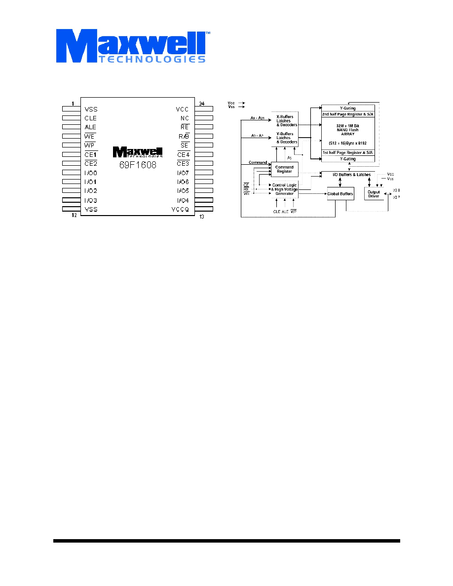
128 Megabit (16M x 8-Bit)
69F1608
©2005 Maxwell Technologies
All rights reserved.
Flash Memory Module
01.07.05 REV 2
F
EATURES
:
∑ Single 5.0 V supply
∑ Organization:
- Memory cell array: (4M + 128k) bit x 8bit
- Data register: (512 + 16) bit x 8bit
-
Contains 4 (32 Megabit) Die
∑ Automatic program and erase
- Page program: (512 + 16) Byte
- Block erase: (8K + 256) Byte
- Status register
∑ 528-Byte page read operation
- Random access: 10 µ s (max)
- Serial page access: 50 ns (min)
∑ Fast write cycle time
- Program time: 250 µ s (typ)
- Block erase time: 2 ms (typ)
∑ Command/address/data multiplexed I/O port
∑ Hardware data protection
- Program/erase lockout during power transitions
∑ Reliable CMOS floating-gate technology
- Endurance: 1,000,000 program/erase cycles
- Data retention: 10 years
∑ Command register operation
D
ESCRIPTION
:
Maxwell Technologies' 69F1608 high-performance flash mem-
ory is a 16M x 8-bit NAND Flash Memory with a spare 128K
(131,072) x 8-bit. A program operation programs the 528-byte
page in 250 µ s and an erase operation can be performed in 2
ms on an 8K-byte block. Data within a page can be read out at
50 ns cycle time per byte. The on-chip write controller auto-
mates all program and erase functions, including pulse repeti-
tion, where required, and internal verify and margining of data.
Even write-intensive systems can take advantage of the
69F1608's extended reliability of 1,000,000 program/erase
cycles by providing either ECC (Error Correction Code) or real
time mapping-out algorithm. These algorithms have been
implemented in many mass storage applications. The spare
16 bytes of a page combined with the other 512 bytes can be
utilized by system-level ECC. The 69F1608 is an optimum
solution for large non-volatile storage applications such as
solid state data storage, digital voice recorders, digital still
cameras and other applications requiring nonvolatility.
Maxwell Technologies' patented R
AD
-P
AK
Æ packaging technol-
ogy incorporates radiation shielding in the microcircuit pack-
age. Capable of surviving in space environments, the
69F1608 is ideal for satellite, spacecraft, and space probe
missions. It is available with packaging and screening up to
Maxwell Technologies self-defined Class K.
Logic Diagram (1 of 4 Die)
2
All data sheets are subject to change without notice
©2005 Maxwell Technologies
All rights reserved.
128 Megabit (16M x 8-Bit) Flash Memory Module
69F1608
01.07.05 REV 2
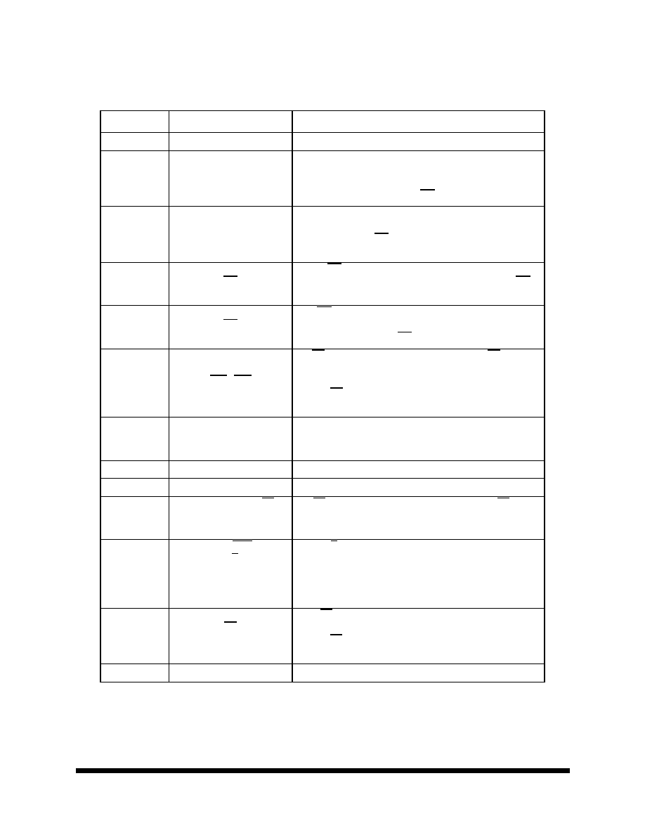
T
ABLE
1. P
INOUT
D
ESCRIPTION
P
IN
S
YMBOL
D
ESCRIPTION
1, 24
V
CC
Supply Voltage
2
Command Latch Enable
(CLE)
The CLE input controls the path activation for commands sent to
the command register. When active high, commands are latched
into the command register through the I/O ports on the rising
edge of the WE signal.
3
Address Latch Enable
(ALE)
The ALE input controls the path activation for address and input
data to the internal address/data register. Addresses are latched
on the rising edge or WE with ALE high, and input data is latched
when ALE is low.
4
Write Enable
(WE)
The WE input controls writes to the I/O port. Commands,
address and data are latched on the rising edge of the WE
pulse.
5
Write Protect
(WP)
The WP pin provides inadvertent write/erase protection during
power transitions. The internal high voltage generator is reset
when the WP pin is active low.
6, 7, 18, 19
Chip Enable Inputs
CE1 - CE4
The CE input is the device selection control. When CE goes high
during a read operation, the device is returned to standby mode.
However, when the device is in the busy state during program or
erase, CE high is ignored, and does not return the device to
standby mode.
8, 9, 10, 11
14, 15, 16, 17
I/O Port:
I/O0 ~I/O7
The I/O pins are used to input command, address and data, and
to output data during read operations. The I/O pins float to High-
Z when the chip is deselected or when the outputs are disabled.
12
V
SS
Ground
13
V
CC
Q
Output Buffer Voltage
20
Spare Area Enable (SE)
The SE input controls the spare area selection when SE is high,
the device is deselected the spare area during Read1, Sequen-
tial data input and page Program.
21
Read/Busy
(R/B)
The R/B output indicates the status of the device operation.
When low, it indicates that a program, erase or random read
operation is in process and returns to high state upon comple-
tion. It is an open drain output and does not float to High-Z condi-
tion when the chip is deselected or when outputs are disabled.
22
Read Enable
(RE)
The RE inputs is the serial data-out control, and when active
drives the data onto the I/O bus. Data is valid t
REA
after the falling
edge of RE which also increments the internal column address
counter by one.
23
NC
No Connection

3
All data sheets are subject to change without notice
©2005 Maxwell Technologies
All rights reserved.
128 Megabit (16M x 8-Bit) Flash Memory Module
69F1608
01.07.05 REV 2
T
ABLE
2. 69F1608 A
BSOLUTE
M
AXIMUM
R
ATINGS
1,2
P
ARAMETER
S
YMBOL
M
IN
M
AX
U
NIT
Voltage on any pin relative to V
SS
V
IN
-0.6
7.0
V
Operating Temperature
T
BIAS
-40
125
∞
C
Storage temperature
T
STG
-65
150
∞
C
Short circuit output current
I
OS
--
5
mA
1. Minimum DC voltage is -0.3 V on input/output pins. During transitions, this level may undershoot to -2.0 V for periods < 30 ns.
Maximum DC voltage on input/output pins is V
CC
+ 0.3 V which, during transitions, may overshoot to V
CC
+ 2.0 V for periods <
20 ns.
2. Permanent device damage may occur if ABSOLUTE MAXIMUM RATINGS are exceeded. Functional operation should be
restricted to the conditions as detailed in the operational sections of this data sheet. Exposure to absolute maximum ratings
conditions for extended periods may affect reliability.
T
ABLE
3. 69F1608 R
ECOMMENDED
O
PERATING
C
ONDITIONS
(V
CC
= 5 V ± 10%, T
A
= -40
TO
125
∞
C)
P
ARAMETER
S
YMBOL
M
IN
T
YP
M
AX
U
NIT
Supply voltage
V
CC
4.5
5.0
5.5
V
Supply voltage
V
SS
0
0
0
V
Input High Voltage
V
IH
2.4
--
V
CC
±0.5
V
Input Low Voltage
V
IL
-0.3
--
0.8
V
T
ABLE
4. D
ELTA
L
IMITS
P
ARAMTER
C
ONDITION
I
CC
1
±10%
I
SB
1
±10%
I
SB
2
±10%
T
ABLE
5. 69F1608 AC T
EST
C
ONDITION
(V
CC
= 5 V ± 10%, T
A
= -40
TO
125
∞
C,
UNLESS
OTHERWISE
NOTED
)
P
ARAMETER
M
IN
M
AX
U
NIT
Input pulse levels
0.4
2.6
V
Input rise times
--
5.0
ns
Input and output timing levels
0.8
2.0
V

4
All data sheets are subject to change without notice
©2005 Maxwell Technologies
All rights reserved.
128 Megabit (16M x 8-Bit) Flash Memory Module
69F1608
01.07.05 REV 2
T
ABLE
6. 69F1608 DC
AND
O
PERATING
C
HARACTERISTICS
(V
CC
= 5 V ± 10%, T
A
= -40
TO
125
∞
C,
UNLESS
OTHERWISE
NOTED
)
P
ARAMETER
S
YMBOL
T
EST
C
ONDITIONS
S
UBGROUPS
M
IN
T
YP
M
AX
U
NIT
Operating current
1
1. Only one (1) CE 1-4 active at a time.
Sequential
read
I
CC1
t
CYCLE
= 80 ns
CEX = V
IL
I
OUT
= 0 mA
1, 2, 3
--
15
30
mA
Program
I
CC2
1, 2, 3
--
15
30
Erase
I
CC3
1, 2, 3
--
25
40
Stand-by-current (TTL)
I
SB1
CE 1-4 = V
IH
WP = SE = 0V or V
CC
1, 2, 3
--
--
4
mA
Stand-by current (CMOS)
I
SB2
CE1-4 = V
CC
- 0.2
WP = SE = 0V or V
CC
1, 2, 3
--
40
400
uA
Input leakage current
2
2. CE1-4 Leakage Current = +/- 10uA.
I
LI
V
IN
= 0 to 5.5 V
1, 2, 3
-40
--
40
uA
Output leakage current
I
LO
V
OUT
= 0 to 5.5 V
1, 2, 3
-40
--
40
uA
Input high voltage, all inputs
V
IH
1, 2, 3
2.0
--
--
V
Input low voltage, all inputs
V
IL
1, 2, 3
--
--
0.8
V
Output high voltage level
V
OH
I
OH
= -400 µ A
1, 2, 3
2.4
--
--
V
Output low voltage level
V
OL
I
OL
= 2.1 mA
1, 2, 3
--
--
0.4
V
Outuput low current (R/B)
I
OL
(R/B)
V
OL
= 0.4 V
1, 2, 3
8
10
--
mA
T
ABLE
7. 69F1608 C
APACITANCE
1
1. Capacitance Guarenteed by design.
P
ARAMETER
S
YMBOL
S
UBGROUPS
T
EST
C
ONDITION
M
IN
M
AX
U
NIT
Input/Output capacitance
C
I/O
4, 5, 6
V
IL
= 0V
--
40
pF
Input capacitance (CE1-4 = 10pF)
C
IN
4, 5, 6
V
IN
= 0V
--
40
pF
T
ABLE
8. 69F1608 M
ODE
S
ELECTION
CLE
ALE
CE
WE
RE
SE
WP
M
ODE
H
L
L
H
X
X
Read Mode
Command Input
L
H
L
H
X
X
Address Input (3
Clock)

5
All data sheets are subject to change without notice
©2005 Maxwell Technologies
All rights reserved.
128 Megabit (16M x 8-Bit) Flash Memory Module
69F1608
01.07.05 REV 2
H
L
L
H
X
H
Write Mode
Command Input
L
H
L
H
X
H
Address Input (3
Clock)
L
L
L
H
L/H
1
H
Data Input
L
L
L
H
L/H
1
X
Sequential Read & Data Output
L
L
L
H
H
L/H
1
X
During Read (Busy)
X
X
X
X
X
L/H
1
H
During Program (Busy)
X
X
X
X
X
X
H
During Erase (Busy)
X
X
2
X
X
X
X
L
Write Protect
X
X
H
X
X
0V/V
CC
3
0V/V
CC
3
Stand-by
1. When SE is high, spare area is deselected.
2. X can be V
IL
or V
IH
.
3. WP should be biased to CMOS high or CMOS low for standby.
T
ABLE
9. 69F1608 P
ROGRAM
/E
RASE
C
HARACTERISTICS
(V
CC
= 5 V ± 10%, T
A
=-40
TO
+125C,
UNLESS
OTHERWISE
NOTED
)
P
ARAMETER
S
YMBOL
M
IN
T
YP
M
AX
U
NIT
Program time
t
PROG
--
0.25
1.5
ms
Number of partial program cycles in the same page
N
OP
--
--
10
cycles
Block erase time
t
BERS
--
2
10
ms
T
ABLE
8. 69F1608 M
ODE
S
ELECTION
CLE
ALE
CE
WE
RE
SE
WP
M
ODE