1
Memory
All data sheets are subject to change without notice
(858) 503-3300 - Fax: (858) 503-3301 - www.maxwell.com
12-Bit A/D Converter
7672
©2002 Maxwell Technologies
All rights reserved.
08.09.02 Rev 13
F
EATURES
:
∑ 12-bit high speed A/D converter
∑ R
AD
-P
AK
Æ radiation-hardened against natural space radia-
tion
∑ Total dose hardness:
- > 100 krad (Si), depending upon space mission
∑ Excellent Single Event Effect
- SEL > 120 Mev/mg/cm
2
- SEU
TH
> 5.8 Mev/mg/cm
2
- SEU
Sat
= -1E-4 cm
2
/Device
∑ Package:
- 24 pin R
AD
-P
AK
Æ flat package
- 24 pin R
AD
-P
AK
Æ DIP
∑ Fast conversion times:
- 7672-05: 5 µs
∑ Low 110 mW typical power consumption
- Corrects all single-bit errors
- Detects all double and some triple-bit errors
∑ High-speed BiCMOS technology
- Choice of +5V and +10V input ranges
- Operates with +5V and -12V power supplies
- Fast 125 ns bus-access time
D
ESCRIPTION
:
Maxwell Technologies
' 7672 high-speed 12-bit analog-to-
digital converter microcircuit features a greater than 100 krad
(Si) total dose tolerance, depending upon space mission. The
7672 uses an accurate high-speed DAC and comparator to
achieve conversion time as low as 5 µs while dissipating only
110 mW of power. The 7672 is designed to be used with an
external reference voltage. This allows the user to choose a
reference whose performance suits the application or to drive
multiple 7672s from a single system reference, since the refer-
ence input is buffered and draws very little current. For digital
signal processing applications where absolute accuracy and
temperature coefficients may be unimportant, a low cost refer-
ence can be used. For optimal precision, a high accuracy ref-
erence where an absolute 12-bit accuracy can be obtained
over a wide temperature range may be used. Analog input
range is pin-selectable for 0 to +5V, 0 to +10V, or ±5V, making
the ADC ideal for data acquisition and analog input/output
cards. A high-speed digital interface (125 ns data access time)
with three state data outputs is compatible with most micro-
processors.
Maxwell Technologies' patented R
AD
-P
AK
Æ packaging technol-
ogy incorporates radiation shielding in the microcircuit pack-
age. It eliminates the need for box shielding while providing
the required radiation shielding for a lifetime in orbit or space
mission. In a GEO orbit, R
AD
-P
AK
provides greater than 100
krad (Si) radiation dose tolerance. This product is available
with screening up to Class S.
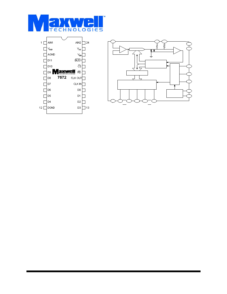
12-BIT DAC
+
-
+
-
SUCCESSIVE APPROXIMATION
REGISTER
CONTROL
LOGIC
CLOCK
OSCILLATOR
12-BIT LATCH
THREE-STATE
OUTPUT DRIVERS
2
1
24
23
22
21
19
20
18
17
4
11
12
13
16
3
V
REF
AIN1
AIN2
V
DD
V
SS
BUSY
CS
RD
CLK OUT
CLK IN
D0
D3
DGND
D4
D11
AGND
Logic Diagram

Memory
2
All data sheets are subject to change without notice
©2002 Maxwell Technologies
All rights reserved.
12-Bit A/D Converter
7672
08.09.02 REV 13
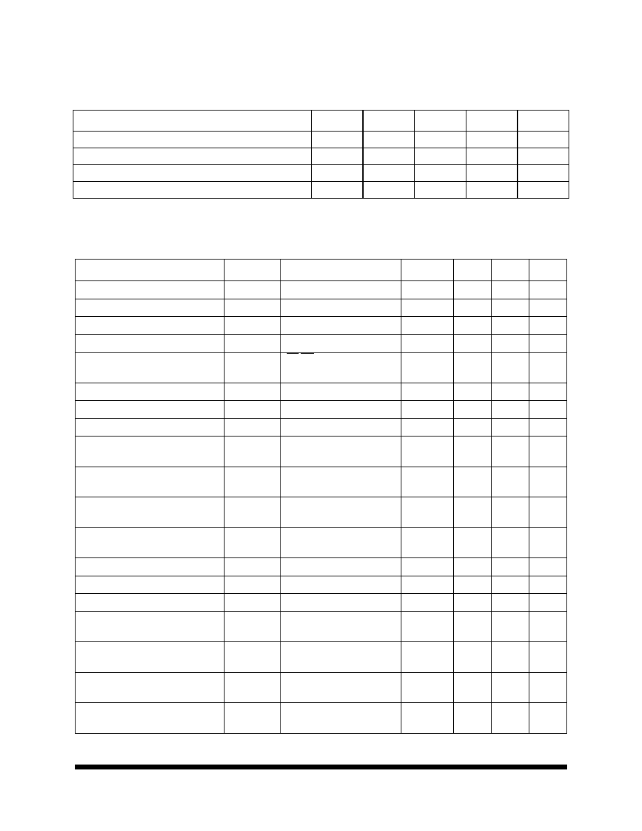
T
ABLE
1. 7672 P
INOUT
D
ESCRIPTION
P
IN
S
YMBOL
D
ESCRIPTION
1
AIN1
Analog Input
2
V
REF
Voltage-Reference Input
3
AGND
Analog Ground
4-11
D11-D4
Three-State Data Outputs
12
DGND
Digital Ground
13-16
D3-D0
Three-State Data Outputs
17
CLKIN
Clock Input
18
CLKOUT
Clock Output
19
RD
READ Input
20
CS
CHIP SELECT
21
BUSY
BUSY
22
V
SS
Negative Supply, -12V
23
V
DD
Positive Supply, +5V
24
AIN2
Analog Input
T
ABLE
2. 7672 A
BSOLUTE
M
AXIMUM
R
ATINGS
P
ARAMETER
S
YMBOL
M
IN
M
AX
U
NITS
Positive Supply Voltage to DGND
V
DD
-0.3
7.0
V
Negative Supply Voltage to DGND
V
SS
-17
+0.3c
V
AGND to DGND
--
-0.3
V
DD
+0.3
V
AIN1, AIN2 to AGND
--
-15
+15
V
Digital Input Voltage to DGND
V
IN
-0.3
V
DD
+0.3
V
Digital Output Voltage to DGND
V
OUT
-0.3
V
DD
+0.3
V
V
REF
to AGND
--
V
SS
-0.3
V
DD
+0.3
V
Power Dissipation to +75∞C
P
D
--
1000
mW
Power Dissipation above 75∞C (Derate)
--
--
10
mW/∞C
Thermal Impedance
JC
--
3.24
∞C/W
Storage Temperature Range
T
STG
-65
+150
∞C
Operating Temperature Range
T
A
-55
+125
∞C
Memory
3
All data sheets are subject to change without notice
©2002 Maxwell Technologies
All rights reserved.
12-Bit A/D Converter
7672
08.09.02 REV 13
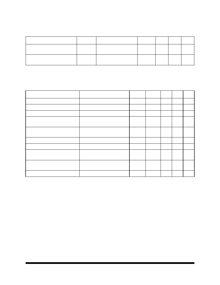
T
ABLE
3. 7672 R
ECOMMENDED
O
PERATING
C
ONDITIONS
P
ARAMETER
S
UBGROUPS
S
YMBOL
M
IN
M
AX
U
NITS
Positive Supply Voltage
1
V
DD
4.75
5.25
V
Negative Supply Voltage
1
V
SS
-13.2
-10.8
V
V
REF
Input Range
1
V
REF
-5.05
-4.95
V
Power Dissipation V
DD
= 5V, V
SS
= -12V
1
P
D
--
179
mW
T
ABLE
4. 7672 DC E
LECTRICAL
C
HARACTERISTICS
(V
DD
= 5V ±5%, V
SS
= -12V ±10%, V
REF
= -5V, T
A
= -55
TO
125 ∞C
UNLESS
OTHERWISE
SPECIFIED
)
P
ARAMETER
S
YMBOL
T
EST
C
ONDITION
S
UBGROUPS
M
IN
M
AX
U
NITS
Input Low Voltage
V
IL
1, 2, 3
--
0.8
V
Input High Voltage
V
IH
1, 2, 3
2.4
--
V
Output Low Voltage
V
OL
I
SINK
= 1.6 mA
1, 2, 3
--
0.4
V
Output High Voltage
V
OH
I
SOURCE
= -200 µA
1, 2, 3
4.0
--
V
Input Leakage Current
I
IN
(CS,RD) V
IN
= V
DD
or GND
(CLKIN) V
IN
= V
DD
or GND
1, 2, 3
--
--
±10
±20
µA
Output Leakage Current
I
LKG
(D0-D11) V
OUT
= V
DD
or GND
1, 2, 3
--
±10
µA
Input Capacitance
1
C
IN
--
10
pF
Floating State Output Capacitance
2
C
OUT
--
15
pF
Power Supply Current
I
DD
I
SS
1, 2, 3
--
--
7
-12
mA
Power Supply Rejection, V
DD
PSRR (V
DD
) V
DD
= 4.75 to 5.25 volts
V
SS
= -12V
1, 2, 3
--
±1
LSB
Power Supply Rejection, V
SS
PSRR (V
SS
) V
SS
= -10.8 to -13.2 volts
V
DD
= 5V
1, 2, 3
--
±1
LSB
Analog Input Current (AIN1 or AIN2)
I
AIN
Unipolar Range: 0 to 5 V, 10V
Bipolar Range: ±5V
1, 2, 3
--
--
±3.5
±1.75
mA
V
REF
Input Range
1
V
REF
1, 2, 3
-5.05
-4.95
V
V
REF
Input Current
I
REF
1, 2, 3
--
±3
µA
Resolution RES
T
A
= -55 to +125∞C
1, 2, 3
12
--
bits
Integral Nonlinearity
INL
T
A
= +25 ∞C
T
A
= -55 to +125∞C
1
2, 3
--
--
±1
±1
LSB
Differential Nonlinearity
DNL
12 bits, no missing codes
T
A
= -55 to +125
∞
C
1, 2, 3
--
±0.9
LSB
Unipolar Offset Error
UOE
T
A
= +25
∞
C
T
A
= -55 to +125
∞
C
1
2, 3
--
--
±5
±6
LSB
Unipolar Gain Error
UGE
T
A
= +25
∞
C
T
A
= -55 to +125
∞
C
1
2, 3
--
--
±5
±7
LSB
Memory
4
All data sheets are subject to change without notice
©2002 Maxwell Technologies
All rights reserved.
12-Bit A/D Converter
7672
08.09.02 REV 13
Bipolar Zero Error
BZE
T
A
= +25
∞
C
T
A
= -55 to +125
∞
C
1
2, 3
--
--
±5
±6
LSB
Bipolar Gain Error
BGE
T
A
= +25
∞
C
T
A
= -55 to +125
∞
C
1
2, 3
--
--
±5
±7
LSB
1. Guaranteed by design.
T
ABLE
5. 7672 T
IMING
C
HARACTERISTICS
1,2
(V
DD
= 5V ±5%, V
SS
= -12V ±10%, V
REF
= -5V, T
A
= -55
TO
125 ∞C
UNLESS
OTHERWISE
SPECIFIED
)
1. 1LSB = FS/4096; T
A
= 25
∞
C; Performance over power supply tolerance is guaranteed by power supply rejection test.
2. All inputs are 0V to +5V swing with t
r
= t
r
= 5ns (10 to 90% of +5V) and timed from a voltage level of +1.6V.
P
ARAMETER
T
EST
C
ONDITION
S
UBGROUPS
S
YMBOL
M
IN
M
AX
U
NITS
Conversion Time, Synchronous Clk,
3
3. Functionally tested.
12.5 clks, TA = -55 to +125 ∞C
9, 10, 11
tCONV
--
5.0
us
Conversion Time, Asynchronous Clk,
12-13 clks, TA = -55 to +125 ∞C
9, 10, 11
tCONV
4.8
5.2
us
CS to RD Setup Time
TA = -55 to +125 ∞C
9, 10, 11
t1
0
--
ns
RD to BUSY Delay
CL = 50 pF, TA = +25 ∞C
CL = 50 pF, TA = -55 to +125 ∞C
9
10, 11
t2
--
--
190
270
ns
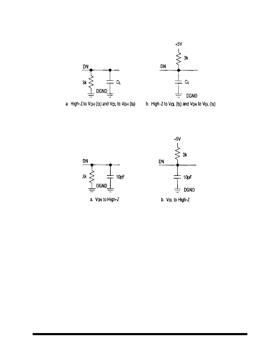
Data Access Time
4
4. t3 and t6 are measured with the load circuits of Figure 1 and are defined as the time required for an output to cross +0.8 or
+2.4.
CL = 100 pF, TA = +25 ∞C
CL = 100 pF, TA = -55 to +125 ∞C
9
10, 11
t3
--
--
125
170
ns
RD Pulse Width
TA = -55 to +125 ∞C
9, 10, 11
t4
t3
--
ns
CS to RD Hold Time
TA = -55 to +125 ∞C
9, 10, 11
t5
0
--
ns
Data Setup Time After BUSY4
CL = 100 pF, TA = +25 ∞C
CL = 100 pF, TA = -55 to +125 ∞C
9
10, 11
t6
--
--
--
70
100
ns
Bus Relinguish Time
5
5. t7 is defined as the time required for the data lines to change 0.5V when loaded with the circuit of Figure 2.
(TA = +25 ∞C)
(-55 < TA < +125 ∞C)
9
10, 11
t7
--
--
75
90
ns
Delay Between Read Operations
(-55 < TA < +125 ∞C)
9, 10, 11
t8
200
--
ns
T
ABLE
4. 7672 DC E
LECTRICAL
C
HARACTERISTICS
(V
DD
= 5V ±5%, V
SS
= -12V ±10%, V
REF
= -5V, T
A
= -55
TO
125 ∞C
UNLESS
OTHERWISE
SPECIFIED
)
P
ARAMETER
S
YMBOL
T
EST
C
ONDITION
S
UBGROUPS
M
IN
M
AX
U
NITS
Memory
5
All data sheets are subject to change without notice
©2002 Maxwell Technologies
All rights reserved.
12-Bit A/D Converter
7672
08.09.02 REV 13
F
IGURE
1. L
OAD
C
IRCUITS
FOR
A
CCESS
T
IME
F
IGURE
2. L
OAD
C
IRCUIT
FOR
B
US
R
ELINQUISH
T
IME