
1
Memory
All data sheets are subject to change without notice
(858) 503-3300 - Fax: (858) 503-3301 - www.maxwell.com
12-Bit A/D Converter
7672
©2002 Maxwell Technologies
All rights reserved.
08.09.02 Rev 13
F
EATURES
:
∑ 12-bit high speed A/D converter
∑ R
AD
-P
AK
Æ radiation-hardened against natural space radia-
tion
∑ Total dose hardness:
- > 100 krad (Si), depending upon space mission
∑ Excellent Single Event Effect
- SEL > 120 Mev/mg/cm
2
- SEU
TH
> 5.8 Mev/mg/cm
2
- SEU
Sat
= -1E-4 cm
2
/Device
∑ Package:
- 24 pin R
AD
-P
AK
Æ flat package
- 24 pin R
AD
-P
AK
Æ DIP
∑ Fast conversion times:
- 7672-05: 5 µs
∑ Low 110 mW typical power consumption
- Corrects all single-bit errors
- Detects all double and some triple-bit errors
∑ High-speed BiCMOS technology
- Choice of +5V and +10V input ranges
- Operates with +5V and -12V power supplies
- Fast 125 ns bus-access time
D
ESCRIPTION
:
Maxwell Technologies
' 7672 high-speed 12-bit analog-to-
digital converter microcircuit features a greater than 100 krad
(Si) total dose tolerance, depending upon space mission. The
7672 uses an accurate high-speed DAC and comparator to
achieve conversion time as low as 5 µs while dissipating only
110 mW of power. The 7672 is designed to be used with an
external reference voltage. This allows the user to choose a
reference whose performance suits the application or to drive
multiple 7672s from a single system reference, since the refer-
ence input is buffered and draws very little current. For digital
signal processing applications where absolute accuracy and
temperature coefficients may be unimportant, a low cost refer-
ence can be used. For optimal precision, a high accuracy ref-
erence where an absolute 12-bit accuracy can be obtained
over a wide temperature range may be used. Analog input
range is pin-selectable for 0 to +5V, 0 to +10V, or ±5V, making
the ADC ideal for data acquisition and analog input/output
cards. A high-speed digital interface (125 ns data access time)
with three state data outputs is compatible with most micro-
processors.
Maxwell Technologies' patented R
AD
-P
AK
Æ packaging technol-
ogy incorporates radiation shielding in the microcircuit pack-
age. It eliminates the need for box shielding while providing
the required radiation shielding for a lifetime in orbit or space
mission. In a GEO orbit, R
AD
-P
AK
provides greater than 100
krad (Si) radiation dose tolerance. This product is available
with screening up to Class S.
12-BIT DAC
+
-
+
-
SUCCESSIVE APPROXIMATION
REGISTER
CONTROL
LOGIC
CLOCK
OSCILLATOR
12-BIT LATCH
THREE-STATE
OUTPUT DRIVERS
2
1
24
23
22
21
19
20
18
17
4
11
12
13
16
3
V
REF
AIN1
AIN2
V
DD
V
SS
BUSY
CS
RD
CLK OUT
CLK IN
D0
D3
DGND
D4
D11
AGND
Logic Diagram
Memory
2
All data sheets are subject to change without notice
©2002 Maxwell Technologies
All rights reserved.
12-Bit A/D Converter
7672
08.09.02 REV 13
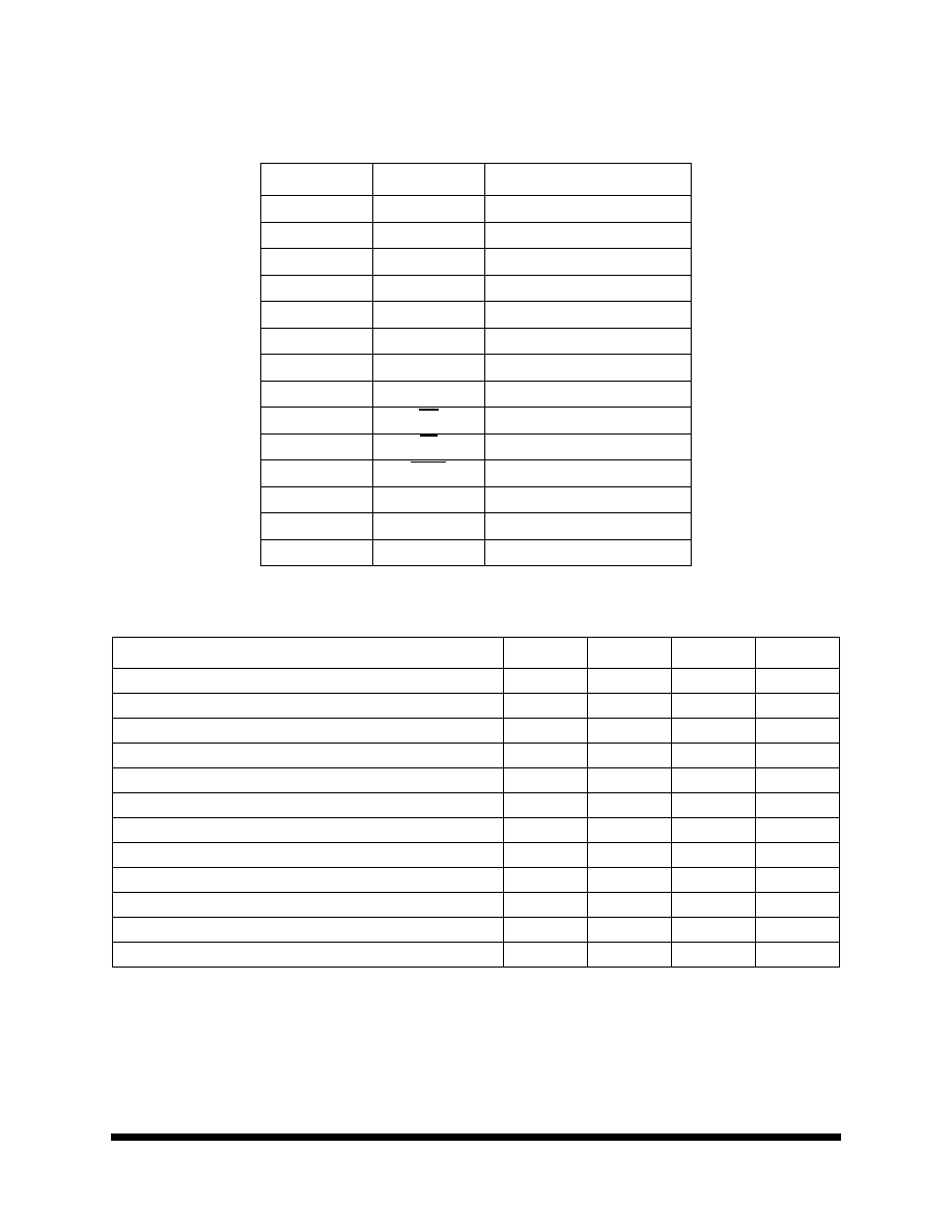
T
ABLE
1. 7672 P
INOUT
D
ESCRIPTION
P
IN
S
YMBOL
D
ESCRIPTION
1
AIN1
Analog Input
2
V
REF
Voltage-Reference Input
3
AGND
Analog Ground
4-11
D11-D4
Three-State Data Outputs
12
DGND
Digital Ground
13-16
D3-D0
Three-State Data Outputs
17
CLKIN
Clock Input
18
CLKOUT
Clock Output
19
RD
READ Input
20
CS
CHIP SELECT
21
BUSY
BUSY
22
V
SS
Negative Supply, -12V
23
V
DD
Positive Supply, +5V
24
AIN2
Analog Input
T
ABLE
2. 7672 A
BSOLUTE
M
AXIMUM
R
ATINGS
P
ARAMETER
S
YMBOL
M
IN
M
AX
U
NITS
Positive Supply Voltage to DGND
V
DD
-0.3
7.0
V
Negative Supply Voltage to DGND
V
SS
-17
+0.3c
V
AGND to DGND
--
-0.3
V
DD
+0.3
V
AIN1, AIN2 to AGND
--
-15
+15
V
Digital Input Voltage to DGND
V
IN
-0.3
V
DD
+0.3
V
Digital Output Voltage to DGND
V
OUT
-0.3
V
DD
+0.3
V
V
REF
to AGND
--
V
SS
-0.3
V
DD
+0.3
V
Power Dissipation to +75∞C
P
D
--
1000
mW
Power Dissipation above 75∞C (Derate)
--
--
10
mW/∞C
Thermal Impedance
JC
--
3.24
∞C/W
Storage Temperature Range
T
STG
-65
+150
∞C
Operating Temperature Range
T
A
-55
+125
∞C
Memory
3
All data sheets are subject to change without notice
©2002 Maxwell Technologies
All rights reserved.
12-Bit A/D Converter
7672
08.09.02 REV 13
T
ABLE
3. 7672 R
ECOMMENDED
O
PERATING
C
ONDITIONS
P
ARAMETER
S
UBGROUPS
S
YMBOL
M
IN
M
AX
U
NITS
Positive Supply Voltage
1
V
DD
4.75
5.25
V
Negative Supply Voltage
1
V
SS
-13.2
-10.8
V
V
REF
Input Range
1
V
REF
-5.05
-4.95
V
Power Dissipation V
DD
= 5V, V
SS
= -12V
1
P
D
--
179
mW
T
ABLE
4. 7672 DC E
LECTRICAL
C
HARACTERISTICS
(V
DD
= 5V ±5%, V
SS
= -12V ±10%, V
REF
= -5V, T
A
= -55
TO
125 ∞C
UNLESS
OTHERWISE
SPECIFIED
)
P
ARAMETER
S
YMBOL
T
EST
C
ONDITION
S
UBGROUPS
M
IN
M
AX
U
NITS
Input Low Voltage
V
IL
1, 2, 3
--
0.8
V
Input High Voltage
V
IH
1, 2, 3
2.4
--
V
Output Low Voltage
V
OL
I
SINK
= 1.6 mA
1, 2, 3
--
0.4
V
Output High Voltage
V
OH
I
SOURCE
= -200 µA
1, 2, 3
4.0
--
V
Input Leakage Current
I
IN
(CS,RD) V
IN
= V
DD
or GND
(CLKIN) V
IN
= V
DD
or GND
1, 2, 3
--
--
±10
±20
µA
Output Leakage Current
I
LKG
(D0-D11) V
OUT
= V
DD
or GND
1, 2, 3
--
±10
µA
Input Capacitance
1
C
IN
--
10
pF
Floating State Output Capacitance
2
C
OUT
--
15
pF
Power Supply Current
I
DD
I
SS
1, 2, 3
--
--
7
-12
mA
Power Supply Rejection, V
DD
PSRR (V
DD
) V
DD
= 4.75 to 5.25 volts
V
SS
= -12V
1, 2, 3
--
±1
LSB
Power Supply Rejection, V
SS
PSRR (V
SS
) V
SS
= -10.8 to -13.2 volts
V
DD
= 5V
1, 2, 3
--
±1
LSB
Analog Input Current (AIN1 or AIN2)
I
AIN
Unipolar Range: 0 to 5 V, 10V
Bipolar Range: ±5V
1, 2, 3
--
--
±3.5
±1.75
mA
V
REF
Input Range
1
V
REF
1, 2, 3
-5.05
-4.95
V
V
REF
Input Current
I
REF
1, 2, 3
--
±3
µA
Resolution RES
T
A
= -55 to +125∞C
1, 2, 3
12
--
bits
Integral Nonlinearity
INL
T
A
= +25 ∞C
T
A
= -55 to +125∞C
1
2, 3
--
--
±1
±1
LSB
Differential Nonlinearity
DNL
12 bits, no missing codes
T
A
= -55 to +125
∞
C
1, 2, 3
--
±0.9
LSB
Unipolar Offset Error
UOE
T
A
= +25
∞
C
T
A
= -55 to +125
∞
C
1
2, 3
--
--
±5
±6
LSB
Unipolar Gain Error
UGE
T
A
= +25
∞
C
T
A
= -55 to +125
∞
C
1
2, 3
--
--
±5
±7
LSB
Memory
4
All data sheets are subject to change without notice
©2002 Maxwell Technologies
All rights reserved.
12-Bit A/D Converter
7672
08.09.02 REV 13
Bipolar Zero Error
BZE
T
A
= +25
∞
C
T
A
= -55 to +125
∞
C
1
2, 3
--
--
±5
±6
LSB
Bipolar Gain Error
BGE
T
A
= +25
∞
C
T
A
= -55 to +125
∞
C
1
2, 3
--
--
±5
±7
LSB
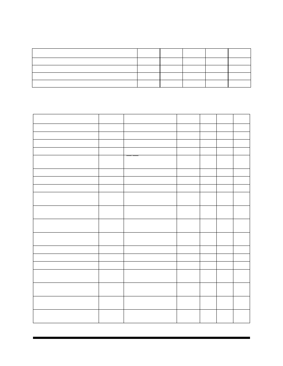
1. Guaranteed by design.
T
ABLE
5. 7672 T
IMING
C
HARACTERISTICS
1,2
(V
DD
= 5V ±5%, V
SS
= -12V ±10%, V
REF
= -5V, T
A
= -55
TO
125 ∞C
UNLESS
OTHERWISE
SPECIFIED
)
1. 1LSB = FS/4096; T
A
= 25
∞
C; Performance over power supply tolerance is guaranteed by power supply rejection test.
2. All inputs are 0V to +5V swing with t
r
= t
r
= 5ns (10 to 90% of +5V) and timed from a voltage level of +1.6V.
P
ARAMETER
T
EST
C
ONDITION
S
UBGROUPS
S
YMBOL
M
IN
M
AX
U
NITS
Conversion Time, Synchronous Clk,
3
3. Functionally tested.
12.5 clks, TA = -55 to +125 ∞C
9, 10, 11
tCONV
--
5.0
us
Conversion Time, Asynchronous Clk,
12-13 clks, TA = -55 to +125 ∞C
9, 10, 11
tCONV
4.8
5.2
us
CS to RD Setup Time
TA = -55 to +125 ∞C
9, 10, 11
t1
0
--
ns
RD to BUSY Delay
CL = 50 pF, TA = +25 ∞C
CL = 50 pF, TA = -55 to +125 ∞C
9
10, 11
t2
--
--
190
270
ns
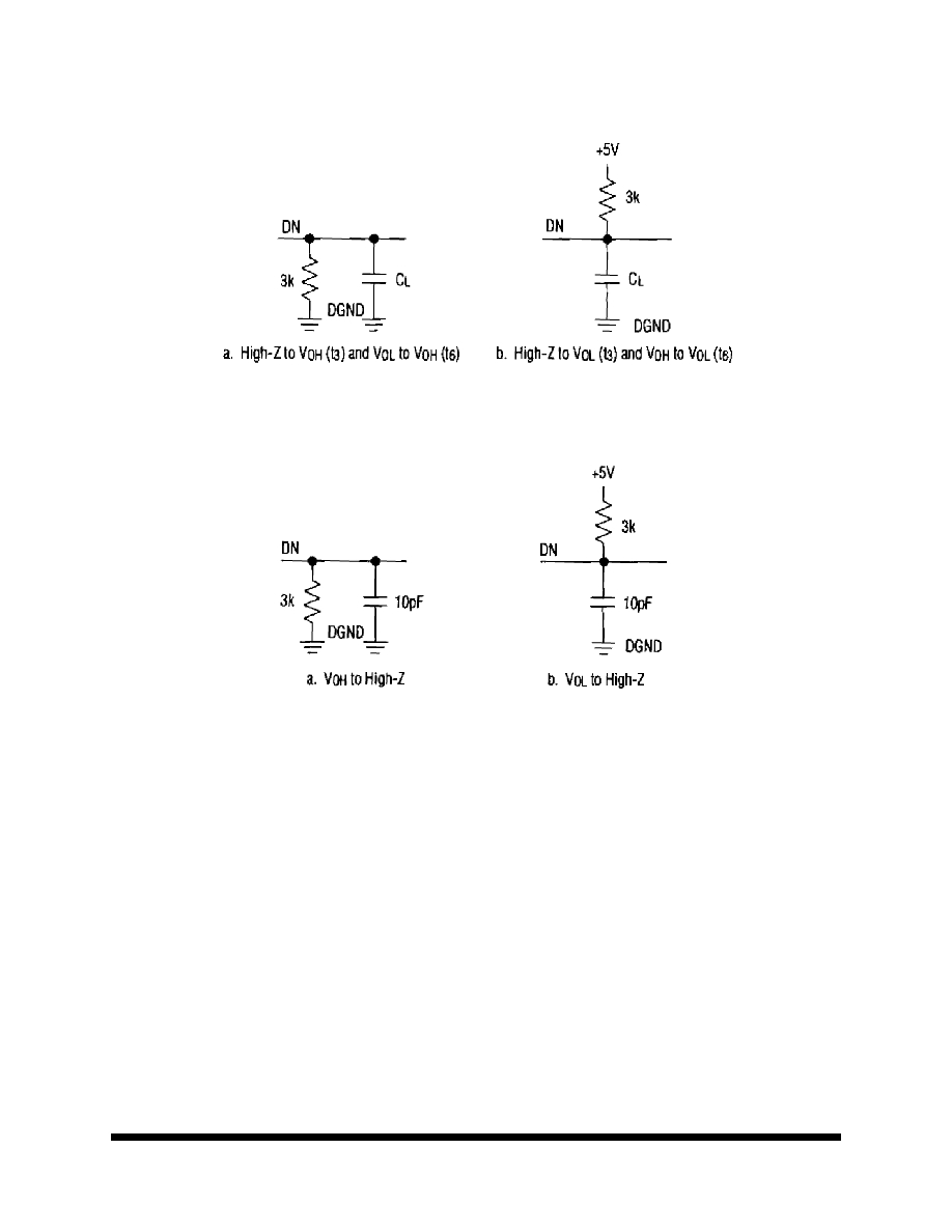
Data Access Time
4
4. t3 and t6 are measured with the load circuits of Figure 1 and are defined as the time required for an output to cross +0.8 or
+2.4.
CL = 100 pF, TA = +25 ∞C
CL = 100 pF, TA = -55 to +125 ∞C
9
10, 11
t3
--
--
125
170
ns
RD Pulse Width
TA = -55 to +125 ∞C
9, 10, 11
t4
t3
--
ns
CS to RD Hold Time
TA = -55 to +125 ∞C
9, 10, 11
t5
0
--
ns
Data Setup Time After BUSY4
CL = 100 pF, TA = +25 ∞C
CL = 100 pF, TA = -55 to +125 ∞C
9
10, 11
t6
--
--
--
70
100
ns
Bus Relinguish Time
5
5. t7 is defined as the time required for the data lines to change 0.5V when loaded with the circuit of Figure 2.
(TA = +25 ∞C)
(-55 < TA < +125 ∞C)
9
10, 11
t7
--
--
75
90
ns
Delay Between Read Operations
(-55 < TA < +125 ∞C)
9, 10, 11
t8
200
--
ns
T
ABLE
4. 7672 DC E
LECTRICAL
C
HARACTERISTICS
(V
DD
= 5V ±5%, V
SS
= -12V ±10%, V
REF
= -5V, T
A
= -55
TO
125 ∞C
UNLESS
OTHERWISE
SPECIFIED
)
P
ARAMETER
S
YMBOL
T
EST
C
ONDITION
S
UBGROUPS
M
IN
M
AX
U
NITS
Memory
5
All data sheets are subject to change without notice
©2002 Maxwell Technologies
All rights reserved.
12-Bit A/D Converter
7672
08.09.02 REV 13
F
IGURE
1. L
OAD
C
IRCUITS
FOR
A
CCESS
T
IME
F
IGURE
2. L
OAD
C
IRCUIT
FOR
B
US
R
ELINQUISH
T
IME
Memory
6
All data sheets are subject to change without notice
©2002 Maxwell Technologies
All rights reserved.
12-Bit A/D Converter
7672
08.09.02 REV 13
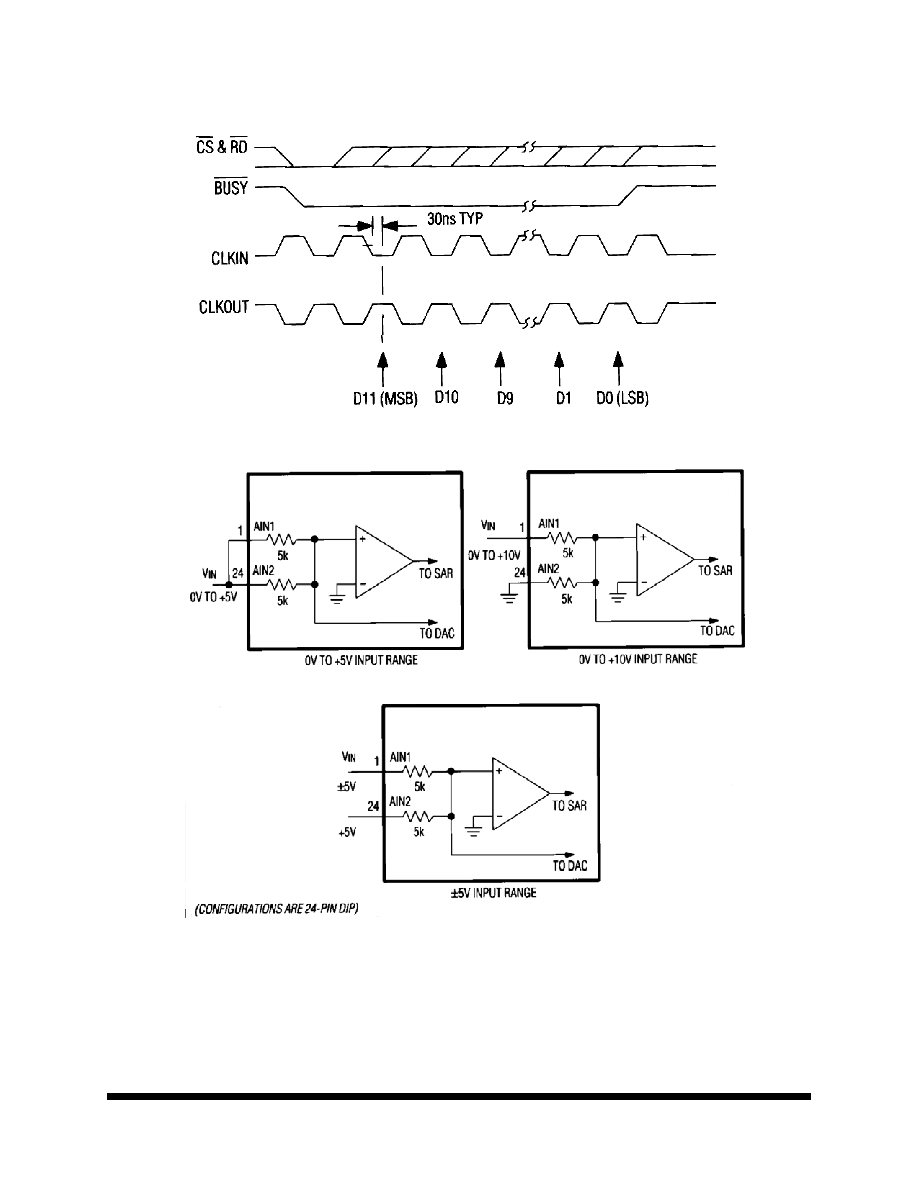
F
IGURE
3.
F
IGURE
4. A
NALOG
I
NPUT
R
ANGE
C
ONFIGURATIONS
Memory
7
All data sheets are subject to change without notice
©2002 Maxwell Technologies
All rights reserved.
12-Bit A/D Converter
7672
08.09.02 REV 13
F
IGURE
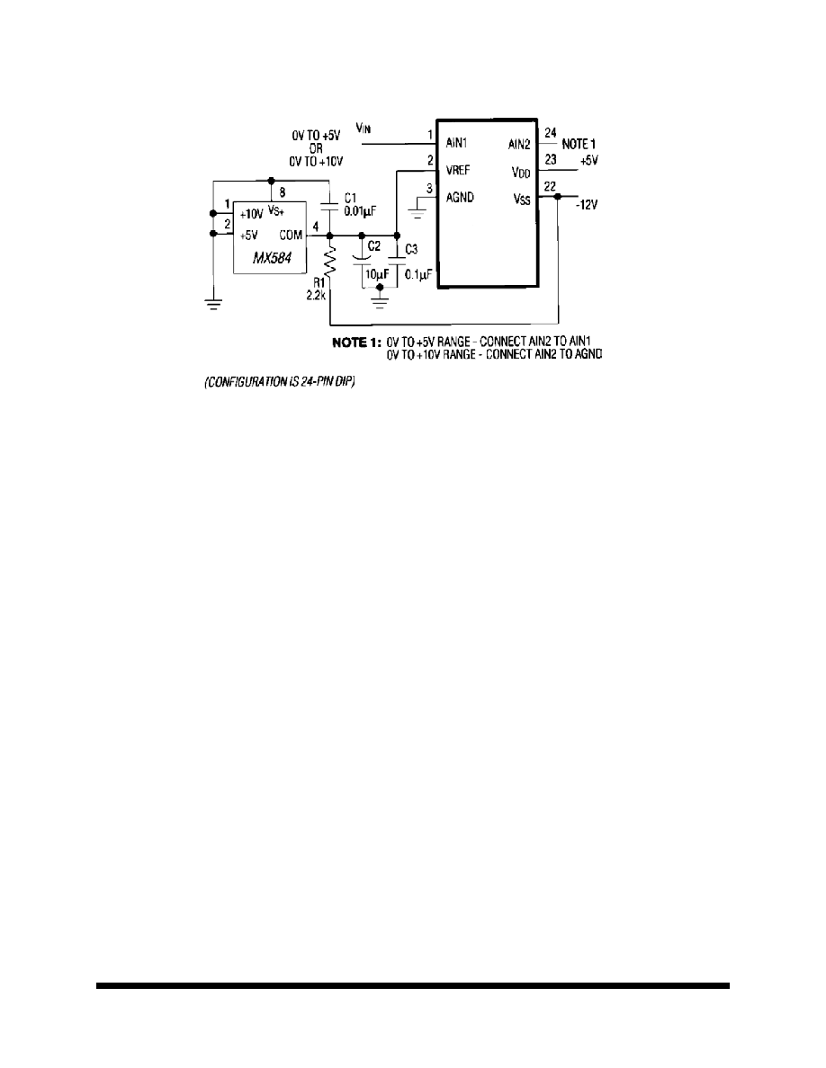
5. U
NIPOLAR
O
PERATING
U
SING
A
R
EFERENCE
Memory
8
All data sheets are subject to change without notice
©2002 Maxwell Technologies
All rights reserved.
12-Bit A/D Converter
7672
08.09.02 REV 13
D24-02
Note: All dimensions in inches
24 P
IN
R
AD
-P
AK
Æ D
UAL
I
N
L
INE
P
ACKAGE
S
YMBOL
D
IMENSION
M
IN
N
OM
M
AX
A
--
0.167
0.200
b
0.014
0.018
0.026
b2
0.045
0.050
0.065
c
0.008
0.010
0.018
D
--
1.200
1.280
E
0.510
0.594
0.620
eA
0.600 BSC
eA/2
0.300 BSC
e
0.100 BSC
L
0.135
0.145
0.155
Q
0.015
0.030
0.045
S1
0.005
0.025
--
S2
0.005
--
--
N
24
Memory
9
All data sheets are subject to change without notice
©2002 Maxwell Technologies
All rights reserved.
12-Bit A/D Converter
7672
08.09.02 REV 13
F24-01
Note: All dimensions in inches
24 P
IN
R
AD
-P
AK
Æ F
LAT
P
ACKAGE
S
YMBOL
D
IMENSION
M
IN
N
OM
M
AX
A
0.153
0.170
0.183
b
0.015
0.017
0.022
c
0.004
0.005
0.009
D
--
0.596
0.640
E
0.350
0.400
0.420
E1
--
--
0.450
E2
0.180
0.236
--
E3
0.030
0.082
--
e
0.050 BSC
L
0.315
0.325
0.335
Q
0.026
0.050
0.056
S1
0.005
0.015
--
N
24

Memory
10
All data sheets are subject to change without notice
©2002 Maxwell Technologies
All rights reserved.
12-Bit A/D Converter
7672
08.09.02 REV 13
Important Notice:
These data sheets are created using the chip manufacturer's published specifications. Maxwell Technologies verifies
functionality by testing key parameters either by 100% testing, sample testing or characterization.
The specifications presented within these data sheets represent the latest and most accurate information available to
date. However, these specifications are subject to change without notice and Maxwell Technologies assumes no
responsibility for the use of this information.
Maxwell Technologies' products are not authorized for use as critical components in life support devices or systems
without express written approval from Maxwell Technologies.
Any claim against Maxwell Technologies must be made within 90 days from the date of shipment from Maxwell Tech-
nologies. Maxwell Technologies' liability shall be limited to replacement of defective parts.

Memory
11
All data sheets are subject to change without notice
©2002 Maxwell Technologies
All rights reserved.
12-Bit A/D Converter
7672
08.09.02 REV 13
Product Ordering Options
Model Number
Feature
Option Details
7672
RP
F
X
Screening Flow
Package
Radiation Feature
Base Product
Nomenclature
Monolithic
S = Maxwell Class S
B = Maxwell Class B
I = Industrial (testing @ -55∞C,
+25∞C, +125∞C)
E = Engineering (testing @ +25∞C)
D = Dual In-line Package (DIP)
F = Flat Pack
RP = R
AD
-P
AK
Æ package
12-Bit A/D Converter
-XX
Access Time
05 = 5 us