
1
M
e
m
o
r
y
All data sheets are subject to change without notice
(858) 503-3300 Fax: (858) 503-3301- www.maxwell.com
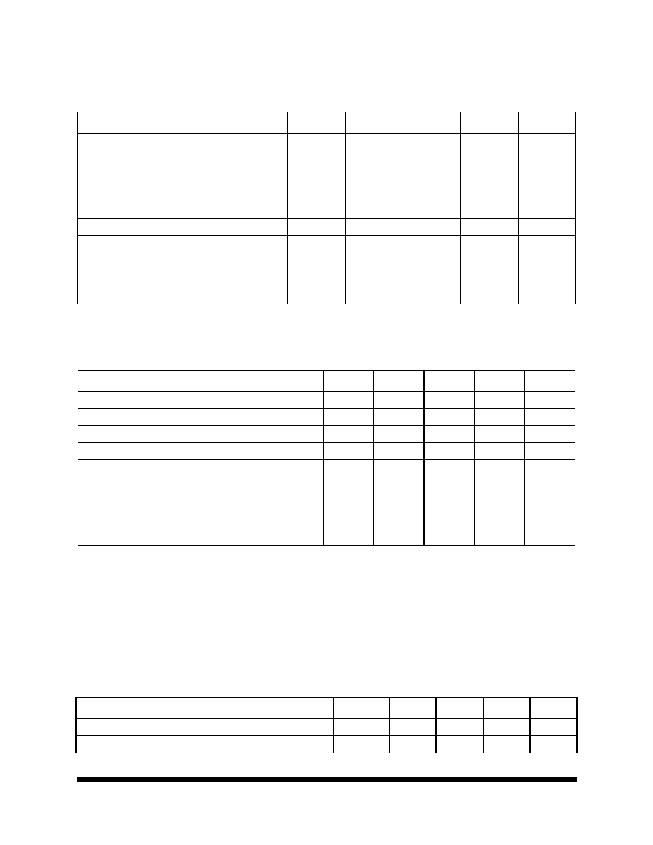
16-Bit Latchup Protected ADC
7805ALP
©2005 Maxwell Technologies
All rights reserved.
01.10.05 Rev 9
F
EATURES
:
∑ 16-bit organization
∑ Latchup Protection TechnologyTM
∑ R
AD
-P
AK
Æ radiation-hardened against natural space radia-
tion
∑ Total dose hardness:
- > 50 krads(Si), depending upon space mission
∑ Latchup converted to reset.
- Rate based on cross section and mission.
∑ Package:
- 28 pin R
AD
-P
AK
Æ flat pack
- 28 pin R
AD
-P
AK
Æ DIP
∑ 100 kHz min sampling rate
∑ Standard ± 10V input range
∑ Advance CMOS technology
- 86 dB min SINAD with 20 kHz input
- Single 5V supply operation
- Utilizes internal or external reference
- Full parallel data output
- Power dissipation: 132 mW max
D
ESCRIPTION
:
Maxwell Technologies' 7805ALP high-speed analog-to-digital
converter features a greater than 50 krad (Si) total dose toler-
ance, depending upon space mission. Using Mawell's radia-
tion-hardened R
AD
-P
AK
Æ packaging technology, the 7805ALP
incorporates the commercial ADS7805 from Burr Brown. This
device is latchup protected by Maxwell Technologies' LPTTM
technology. The 7805ALP, 16-bit sampling CMOS A/D . The
device contains a complete 16-bit capacitor-based SAR A/D
with S/H, reference, clock, interface for microprocessor use,
and three-state output drivers. The 7805ALP is specified at a
100 kHz sampling rate, and guaranteed over the full tempera-
ture range. Laser-trimmed scaling resistors provide an indus-
try-standard ± 10V input range, while the innovative design
allows operation from a single 5V supply, with power dissipa-
tion of under 132 mW.
Maxwell Technologies' patented R
AD
-P
AK
Æ packaging technol-
ogy incorporates radiation shielding in the microcircuit pack-
age. It eliminates the need for box shielding while providing
the required radiation shielding for a lifetime in orbit or space
mission. In a GEO orbit, R
AD
-P
AK
Æ provides greater than 50
krad (Si) radiation dose tolerance. This product is available
with screening up to Maxwell Technologies self-defiened
Class K.
Logic Diagram

M
e
m
o
r
y
2
All data sheets are subject to change without notice
©2005 Maxwell Technologies
All rights reserved.
16-Bit Latchup Protected ADC
7805ALP
01.10.05 Rev 9
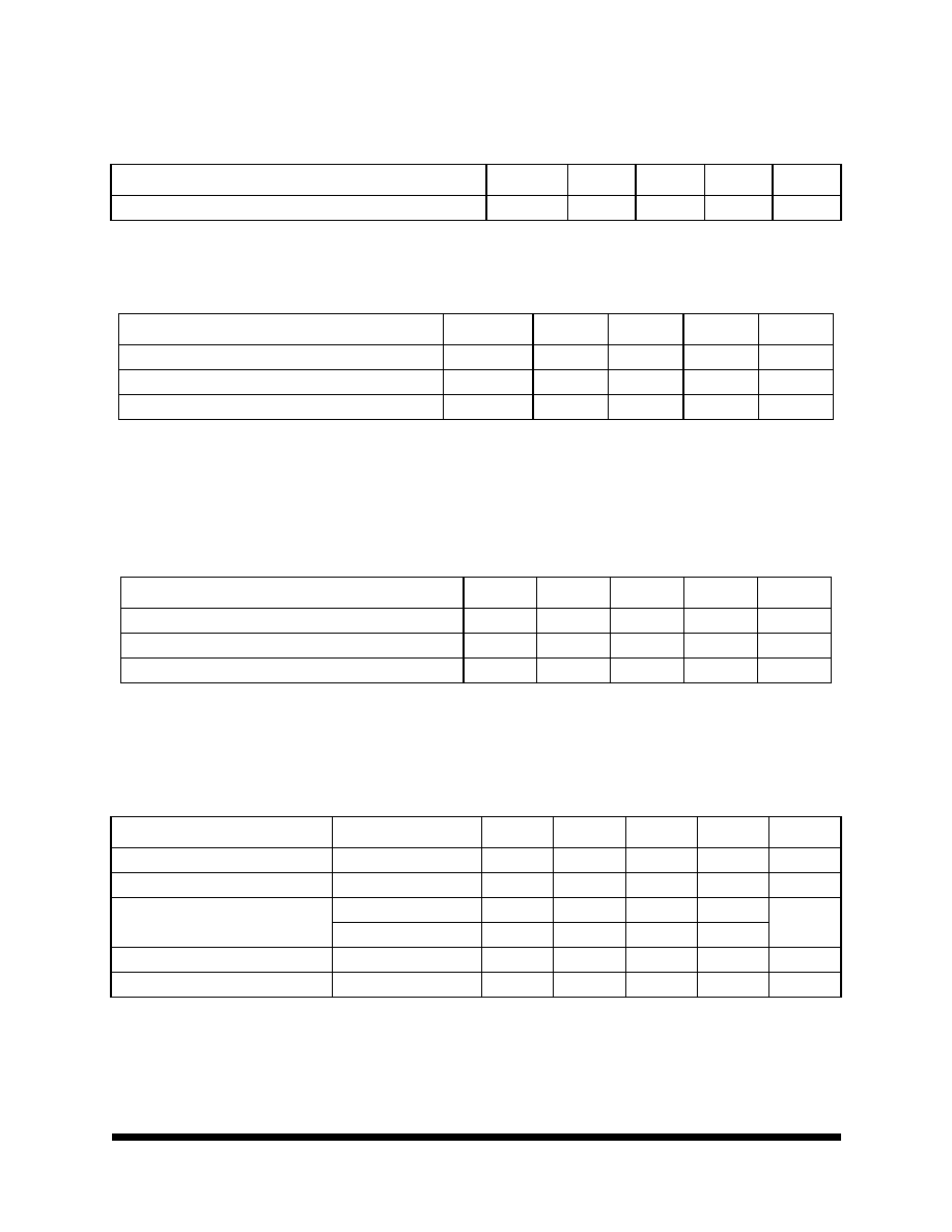
T
ABLE
1. 7805ALP P
INOUT
D
ESCRIPTION
P
IN
N
UMBER
N
AME
D
IGITAL
I/O
D
ESCRIPTION
1
V
IN
Analog input.
2
AGND1
Analog ground. Used internally as ground reference point.
3
REF
Reference input/output. 2.2 µ F tantalum capacitor to ground
4
CAP
Reference buffer capacitor. 2.2 µ F tantalum capacitor to ground.
5
AGND2
Analog ground.
6
D15 (MSB)
0
Data bit 15. Most Significant Bit (MSB) of conversion results. When STATUS is
HIGH*, D15 must not be driven high.
7
D14
0
Data bit 14. When STATUS is HIGH*, D14 must not be driven high.
8
D13
0
Data bit 13. When STATUS is HIGH*, D13 must not be driven high.
9
D12
0
Data bit 12. When STATUS is HIGH*, D12 must not be driven high.
10
D11
0
Data bit 11. When STATUS is HIGH*, D11 must not be driven high.
11
D10
0
Data bit 10. When STATUS is HIGH*, D10 must not be driven high.
12
D9
0
Data bit 9. When STATUS is HIGH*, D9 must not be driven high.
13
D8
0
Data bit 8. When STATUS is HIGH*, D8 must not be driven high.
14
DGND
Digital Ground
15
D7
0
Data bit 7. When STATUS is HIGH*, D7 must not be driven high.
16
D6
0
Data bit 6. When STATUS is HIGH*, D6 must not be driven high.
17
D5
0
Data bit 5. When STATUS is HIGH*, D5 must not be driven high.
18
D4
0
Data bit 4. When STATUS is HIGH*, D4 must not be driven high.
19
D3
0
Data bit 3. When STATUS is HIGH*, D3 must not be driven high.
20
D2
0
Data bit 2. When STATUS is HIGH*, D2 must not be driven high.
21
D1
0
Data bit 1. When STATUS is HIGH*, D1 must not be driven high.
22
D0 (LSB)
0
Data bit 0. Least Significant Bit (LSB) of conversion results. When STATUS is
HIGH*, D0 must not be driven high.
23
STATUS*
0
STATUS when HIGH indicates latchup protection is active and output data is
invalid. Capacitive loading should not exceed 1000 pF.
24
R/C
I
With CS LOW and BUSY HIGH, a falling edge of R/C initiates a new conversion.
When STATUS is HIGH*, CS and R/C must not be driven high.
25
CS
I
Internally OR'd with R/C. If R/C LOW, a falling edge on CS initiates a new conver-
sion. When STATUS is HIGH*, CS and R/C must not be driven high.
26
BUSY
0
At the start of a conversion, BUSY goes LOW and stays LOW until the conversion
is completed and the digital outputs have been updated.
27
DECPLNG
Supply voltage high speed decoupling pin. Decouple to ground with 1.0 µ F ceramic
capacitor.
28
V
S
Supply input. Nominally 5V. Decouple to ground with 10 µ F tantalum capacitor.
M
e
m
o
r
y
3
All data sheets are subject to change without notice
©2005 Maxwell Technologies
All rights reserved.
16-Bit Latchup Protected ADC
7805ALP
01.10.05 Rev 9
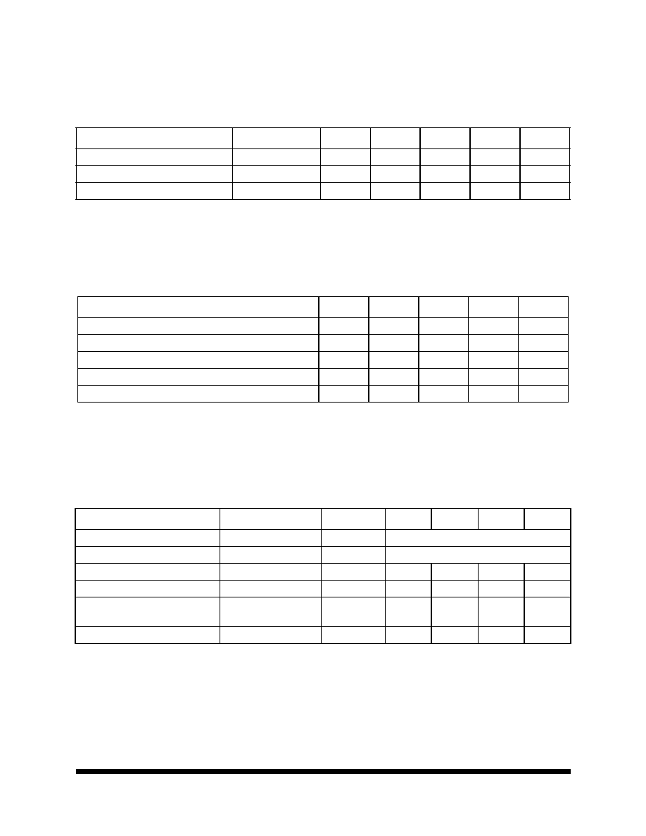
T
ABLE
2. 7805ALP A
BSOLUTE
M
AXIMUM
R
ATINGS
P
ARAMETER
S
YMBOL
M
IN
T
YP
M
AX
U
NIT
Analog Inputs
V
IN
CAP
REF
-25
V
S
9
--
--
--
25
AGND2 - 0.3
--
V
Ground Voltage Difference
DGND
AGND1
AGND2
-0.3
-0.3
-0.3
--
--
--
0.3
0.3
0.3
V
Supply Input
V
S
--
7
V
Digital Inputs
-0.3
--
VS + 0.3
V
Thermal Impedance
JC
11
∞
C/W
Internal Power Dissipation
--
--
825
mW
Maximum Junction Temperature
T
J
--
--
165
∞
C
T
ABLE
3. 7805ALP DC A
CCURACY
S
PECIFICATIONS
(V
S
= 5V, T
A
= -40
TO
+85
∞
C U
NLESS
O
THERWISE
S
PECIFIED
)
P
ARAMETER
C
ONDITIONS
S
UBGROUPS
M
IN
T
YP
M
AX
U
NIT
Integral Linearity Error
--
--
±3
LSB
Differential Linearity Error
--
--
4, -1
LSB
No Missing Codes
1
1. Guaranteed by design
15
--
--
Bits
Transition Noise
2
2. Typical rms noise at worst case transitions and temperatures.
--
1.3
--
LSB
Full Scale Error
3,4
3. Measured with various fixed resistors.
4. Full scale error is worst case - Full Scale or +Full Scale untrimmed deviation from ideal first and last code transitions, divided
by the transition voltage (not divided by the full-scale range) and included the effect of offset error.
--
--
±0.5
%
Full Scale Error Drift
--
±7
--
ppm/
∞
C
Bipolar Zero Error
3
--
--
±10
mV
Bipolar Zero Error Drift
--
±2
--
ppm/
∞
C
Power Supply Sensitivity
4.8V < V
S
< 5.25V
--
--
±8
LSB
T
ABLE
4. 7805ALP D
IGITAL
I
NPUTS
(V
S
= 5V, T
A
= -40
TO
+85
∞
C U
NLESS
O
THERWISE
S
PECIFIED
)
P
ARAMETER
S
UBGROUPS
M
IN
T
YP
M
AX
U
NIT
V
IL
1, 2, 3
-0.3
--
0.8
V
V
IH
2.0
--
V
S
+0.3
V
M
e
m
o
r
y
4
All data sheets are subject to change without notice
©2005 Maxwell Technologies
All rights reserved.
16-Bit Latchup Protected ADC
7805ALP
01.10.05 Rev 9
I
IL
, I
IH
1, 2, 3
--
--
±10
µ A
T
ABLE
5. 7805ALP A
NALOG
I
NPUTS
(V
S
= 5V, T
A
= -40
TO
+85
∞
C U
NLESS
O
THERWISE
S
PECIFIED
)
P
ARAMETER
S
UBGROUPS
M
IN
T
YP
M
AX
U
NIT
Voltage Ranges
1
1. Tested by application of signal.
1, 2, 3
-10
±10
10
V
Impedance
1, 2, 3
--
23
--
k
Capacitance
2
2. Guarenteed by design
--
--
35
--
pF
T
ABLE
6. 7805ALP T
HROUGHPUT
S
PEED
(V
S
= 5V, T
A
= -40
TO
+85
∞
C U
NLESS
O
THERWISE
S
PECIFIED
)
P
ARAMETER
S
UBGROUPS
M
IN
T
YP
M
AX
U
NIT
Conversion Time
9, 10, 11
--
7.6
8
µ s
Complete Cycle (Acquire and Convert)
9, 10, 11
--
--
10
µ s
Throughput Rate
1
1. Guaranteed by design
100
--
--
kHz
T
ABLE
7. 7805ALP AC A
CCURACY
S
PECIFICATIONS
(V
S
= 5V, T
A
= -40
TO
+85
∞
C U
NLESS
O
THERWISE
S
PECIFIED
)
P
ARAMETER
T
EST
C
ONDITIONS
S
UBGROUPS
M
IN
T
YP
M
AX
U
NIT
Spurious-Free Dynamic Range
1,2
1. All specifications in dB are referred to a full-scale 10V input.
2. Guaranteed by design.
f
IN
= 45 kHz
4, 5, 6
90
--
--
dB
Total Harmonic Distortion
1,2
f
IN
= 45 kHz
4, 5, 6
--
--
-90
dB
Signal-to-(Noise + Distortion)
1,2
f
IN
= 45 kHz
4, 5, 6
83
--
--
dB
-60dB Input
4, 5, 6
--
30
--
Signal-to-Noise
1,2
f
IN
= 45 kHz
4, 5, 6
83
--
--
dB
Full-Power Bandwidth
3
3. Full-power bandwidth defined as full-scale input frequency at which signal-to-(noise + distortion) degrades to 60 dB or 10 bits of
accuracy.
4, 5, 6
--
250
--
kHz
T
ABLE
4. 7805ALP D
IGITAL
I
NPUTS
(V
S
= 5V, T
A
= -40
TO
+85
∞
C U
NLESS
O
THERWISE
S
PECIFIED
)
P
ARAMETER
S
UBGROUPS
M
IN
T
YP
M
AX
U
NIT
M
e
m
o
r
y
5
All data sheets are subject to change without notice
©2005 Maxwell Technologies
All rights reserved.
16-Bit Latchup Protected ADC
7805ALP
01.10.05 Rev 9
T
ABLE
8. 7805ALP S
AMPLING
D
YNAMICS
(V
S
= 5V, T
A
= -40
TO
+85
∞
C U
NLESS
O
THERWISE
S
PECIFIED
)
P
ARAMETER
T
EST
C
ONDITIONS
S
UBGROUPS
M
IN
T
YP
M
AX
U
NIT
Aperture Delay
9, 10, 11
--
40
--
nS
Transient Response
FS Step
9, 10, 11
--
2
--
µ S
Overvoltage Recovery
1
1. Recovers to specified performance after 2 x f
S
input overvoltage.
9, 10, 11
--
150
--
nS
T
ABLE
9. 7805ALP R
EFERENCE
T
ABLE
10.
(V
S
= 5V, T
A
= -40
TO
+85
∞
C U
NLESS
O
THERWISE
S
PECIFIED
)
P
ARAMETER
S
UBGROUPS
M
IN
T
YP
M
AX
U
NIT
Internal Reference Voltage
1, 2, 3
2.48
2.5
2.52
V
Internal Reference Source Current (Must use external buffer)
1, 2, 3
--
1
--
µ A
Internal Reference Drift
1, 2, 3
--
8
--
ppm/
∞
C
External Reference Voltage Range for Specified Linearity
1
1. Tested by application of signal.
1, 2, 3
--
2.5
--
V
External Reference Current Drain
2
2. Guaranteed by design
--
--
--
100
µ A
T
ABLE
11. 7805ALP D
IGITAL
O
UTPUTS
(V
S
= 5V, T
A
= -40
TO
+85
∞
C U
NLESS
O
THERWISE
S
PECIFIED
)
P
ARAMETER
T
EST
C
ONDITIONS
S
UBGROUPS
M
IN
T
YP
M
AX
U
NIT
Data Formatting
(Parallel 16-bits Binary Two's Complement)
Data Coding
Binary Two's Complement
V
OL
(I
SINK
= 1.6mA) 4.0
1, 2, 3
--
--
0.4
V
V
OH
(I
SOURCE
= -400 µ A)
1, 2, 3
4.0
--
--
V
Leakage Current
High-Z State, V
OUT
= 0V
to V
S
1, 2, 3
--
--
±5
µ A
Output Capacitance
1
1. Guarenteed by design
High-Z State
--
--
10
--
pF