1
M
e
m
o
r
y
All data sheets are subject to change without notice
(858) 503-3300 - Fax: (858) 503-3301 - www.maxwell.com
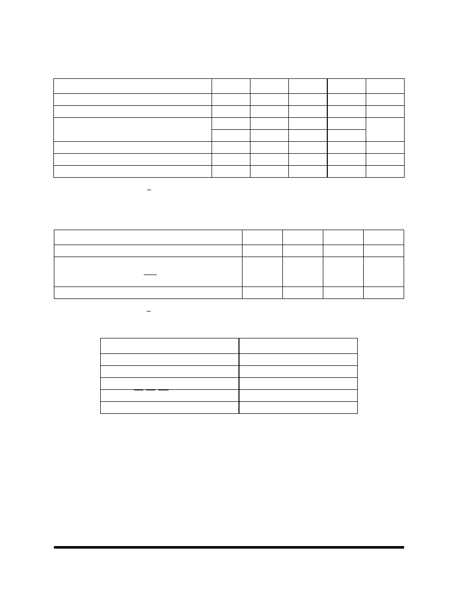
8 Megabit (256K x 32-Bit)
Low Voltage EEPROM MCM
79LV0832
©2005 Maxwell Technologies
All rights reserved.
01.10.05 Rev 8
F
EATURES
:
∑ 256k x 32-bit EEPROM MCM
∑ R
AD
-P
AK
Æ radiation-hardened against natural
space radiation
∑ Total dose hardness:
- >100 krad (Si)
- Dependent upon orbit
∑ Excellent Single event effects
- SEL
TH
> 84.7 MeV/mg/cm
2
- SEU > 26.6 MeV/mg/cm
2
read mode
- SEU = 11.4 MeV/mg/cm
2
write mode
∑ High endurance
- 10,000 cycles/dword, 10 year data retention
∑ Page Write Mode: 2 X 128 dword page
∑ High Speed:
- 200 and 250 ns maximum access times
∑ Automatic programming
- 15 ms automatic Page/dword write
D
ESCRIPTION
:
Maxwell Technologies' 79LV0832 multi-chip module (MCM)
memory features a greater than 100 krad (Si) total dose toler-
ance, dependent upon orbit. Using Maxwell Technologies' pat-
ented radiation-hardened R
AD
-P
AK
Æ MCM packaging
technology, the 79LV0832 is the first radiation-hardened 8
megabit MCM EEPROM for space application. The 79LV0832
uses eight 1 Megabit high speed CMOS die to yield an 8
megabit product. The 79LV0832 is capable of in-system elec-
trical dword and page programmability. It has a 128 x 32 byte
page programming function to make its erase and write opera-
tions faster. It also features Data Polling and a Ready/Busy
signal to indicate the completion of erase and programming
operations. In the 79LV0832, hardware data protection is pro-
vided with the RES pin. Software data protection is imple-
mented using the JEDEC standard algorithm.
Maxwell Technologies' patented R
AD
-P
AK
Æ packaging technol-
ogy incorporates radiation shielding in the microcircuit pack-
age. It eliminates the need for box shielding while providing
the required radiation shielding for a lifetime in orbit or space
mission. In a GEO orbit, R
AD
-P
AK
Æ` provides greater than 100
krad (Si) radiation dose tolerance. This product is available
with screening up to MAxwell Technologies self-defined Class
K.

M
e
m
o
r
y
2
01.10.05 Rev 8
All data sheets are subject to change without notice
©2005 Maxwell Technologies
All rights reserved
Low Voltage 8 Megabit (256K x 32-Bit) EEPROM MCM
79LV0832
T
ABLE
1. 79LV0832 P
INOUT
D
ESCRIPTION
P
IN
S
YMBOL
D
ESCRIPTION
84-77, 29-37
ADDR0 to ADDR16
Address Input
48-55, 66-73, 96,
1-7, 18-25
I/O0 to I/O31
Data Input/Output
61
OE
Output Enable
41, 43
CE0-1
Chip Enable 0 through 1
45
WE
Write Enable
10, 17, 28, 40, 44,
58, 65, 76, 87, 93
3.3V
Power Supply
8, 9, 11-16, 26, 27,
38, 42, 46, 56, 57,
59, 60, 62-64, 74,
75, 85, 86, 88-92,
94, 95
GND
Ground
39
RDY/BUSY
Ready/Busy
47
RES
Reset
M
e
m
o
r
y
3
01.10.05 Rev 8
All data sheets are subject to change without notice
©2005 Maxwell Technologies
All rights reserved
Low Voltage 8 Megabit (256K x 32-Bit) EEPROM MCM
79LV0832
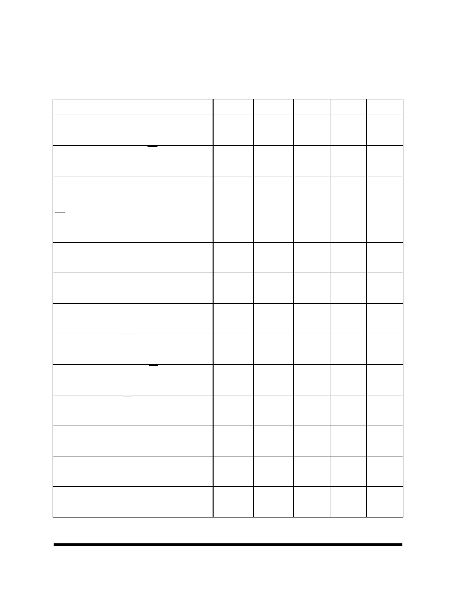
T
ABLE
2. 79LV0832 A
BSOLUTE
M
AXIMUM
R
ATINGS
P
ARAMETER
S
YMBOL
M
IN
TYP
M
AX
U
NIT
Supply Voltage
V
CC
-0.6
7.0
V
Input Voltage
V
IN
-0.5
1
1. V
IN
min = -3.0V for pulse width <50ns.
7.0
V
Package Weight
RP
45
Grams
RT
38
Thermal Impedance (RP and RT Packages; XP TBD)
F
JC
3
∞
C/W
Operating Temperature Range
T
OPR
-55
125
∞
C
Storage Temperature Range
T
STG
-65
150
∞
C
T
ABLE
3. 79LV0832 R
ECOMMENDED
DC O
PERATING
C
ONDITIONS
P
ARAMETER
S
YMBOL
M
IN
M
AX
U
NIT
Supply Voltage
V
CC
3.0
3.6
V
Input Voltage
RES_PIN
V
IL
V
IH
V
H
-0.3
1
2.2
V
CC
-0.5
1. V
IL
min = -1.0V for pulse width < 50 ns
0.8
V
CC
+0.3
V
CC
+1
V
V
V
Operating Temperature Range
T
OPR
-55
125
∞
C
T
ABLE
4. D
ELTA
L
IMITS1
1. Delta limits are calculated from test data taken at preburn-in and post burn-in as
defined in MIL-STD-883
P
ARAMETER
V
ARIATION2
2. Specified value in Table 6
I
CC1A
+/- 10 %
I
CC2A
+/- 10 %
I
CC2C
+/- 10 %
I
LI
- ADDR, CE, OE, WE
+/- 10 %
I
Lo
- D0 - D31
+/- 10 %

M
e
m
o
r
y
4
01.10.05 Rev 8
All data sheets are subject to change without notice
©2005 Maxwell Technologies
All rights reserved
Low Voltage 8 Megabit (256K x 32-Bit) EEPROM MCM
79LV0832
T
ABLE
5. 79LV0832 C
APACITANCE
(T
A
= 25
∞
C, f = 1 MHz)
P
ARAMETER
S
YMBOL
M
IN
M
AX
U
NIT
Input Capacitance: V
IN
= 0V
1
C
IN
--
6
pF
C
IN
OE
--
6
C
IN
WE
--
6
C
IN
CE
0-1
--
6
C
IN
A0-A16
--
6
C
IN
RES
--
48
Output Capacitance: V
OUT
= 0V
1
C
Out
RDY/BSY
--
6
pF
C
O ut
D0-D31
--
12
1. Guaranteed by design.
T
ABLE
6. 79LV0832 DC E
LECTRICAL
C
HARACTERISTICS
(V
CC
= 3.3V ±10%, T
A
= -55
TO
+125∞C)
P
ARAMETER
T
EST
C
ONDITION
S
YMBOL
S
UBGROUPS
M
IN
M
AX
U
NITS
Input Leakage Current
1
A0-A16, CE,WE, OE
V
IN
= V
CC
I
LI
1, 2, 3
--
4
2
µ A
V
IN
=V
IH
720
2
µ A
V
IN
=0V
720
2
µ A
Input Leakage Current
D0-D31
V
IN
=V
CC
I
LI
1, 2, 3
4
µ A
Output Leakage Current (V
CC
= 3.6V, V
OUT
= 3.6V/0.4V)
I
LO
1, 2, 3
--
4
µ A
Standby V
CC
Current
1
CE = ADDR=WE=OE =V
CC
I
CC1A
1, 2, 3
--
80
µ A
CE = ADDR=WE=OE =V
IH
I
CC1B
--
15
mA
CE = V
IH
; ADDR=WE=OE =0V
I
CC1C
--
15
mA
Operating
V
CC
Current
1,3
OE = 0V; ADDR=WE=V
CC
I
OUT
= 0mA, CE Duty = 100%,
Cycle = 1 us at V
CC
= 3.6V
I
CC2A
1, 2, 3
24
mA
OE =ADDR=WE=0V
I
OUT
= 0mA, CE Duty = 100%,
Cycle = 1 us at V
CC
= 3.6V
I
CC2B
1, 2, 3
--
40
mA
OE = 0V; ADDR=WE=V
CC
I
OUT
= 0mA, CE Duty = 100%,
Cycle = 200 ns at V
CC
=3.6V
I
CC2C
1, 2, 3
60
mA
OE =ADDR=WE=0V
I
OUT
= 0mA, CE Duty = 100%,
Cycle = 200 ns at V
CC
= 3.6V
I
CC2D
1, 2, 3
--
100
mA
Input Voltage
RES_PIN
V
IL
V
IH
V
H
1, 2, 3
2.2
V
CC
-0.5
0.8
V
M
e
m
o
r
y
5
01.10.05 Rev 8
All data sheets are subject to change without notice
©2005 Maxwell Technologies
All rights reserved
Low Voltage 8 Megabit (256K x 32-Bit) EEPROM MCM
79LV0832
Output Voltage
Data Lines: V
CC
Min, I
OL
= 2.1mA
RDY/BSY_Line: V
CC
Min, I
OL
= 12mA
Data Lines: V
CC
Min, I
OH
= -400µ A
RDY/BSY_Line: V
CC
Min, I
OH
= -12mA
All Outputs: V
CC
Min, I
OH
=-100uA
V
OL
V
OL
V
OH
V
OH
1, 2, 3
--
2.4
2.4
V
CC
-0.3V
0.4
0.4
--
--
V
V
V
V
V
1. All Inputs are tied to Vcc with a 5.5K
W resistor, except for RES which is 30KW.
2. For RES I
LI
=800uA max.
3. Only one CE active (low) at a time
T
ABLE
7. 79LV0832 AC E
LECTRICAL
C
HARACTERISTICS
FOR
R
EAD
O
PERATION
1
(V
CC
= 3.3V ±10%, T
A
= -55
TO
+125∞C)
P
ARAMETER
S
YMBOL
S
UBGROUPS
M
IN
M
AX
U
NIT
Address Access Time CE = OE = V
IL
, WE = V
IH
-200
-250
t
ACC
9, 10, 11
--
--
200
250
ns
Chip Enable Access Time OE = V
IL
, WE = V
IH
-200
-250
t
CE
9, 10, 11
--
--
200
250
ns
Output Enable Access TIme CE = V
IL
, WE = V
IH
-200
-250
t
OE
9, 10, 11
0
0
110
120
ns
Output Hold to Address Change CE = OE =V
IL
, WE = V
IH
-200
-250
t
OH
9, 10, 11
0
0
--
--
ns
Output Disable to High-Z
2
CE = V
IL
, WE = V
IH
-200
-250
CE = OE = V
IL
, WE = V
IH
-200
-250
t
DF
t
DFR
9, 10, 11
0
0
0
0
50
50
300
350
ns
ns
RES to Output Delay CE = OE = V
IL
, WE = V
IH
3
-200
-250
T
RR
9, 10, 11
0
0
525
550
ns
1. Test conditions: input pulse levels = 0.4V to 2.2V; input rise and fall times < 20 ns; output load = 1 TTL gate + 100 pF (including
scope and jig); reference levels for measuring timing = 0.8 V/1.8 V.
2. t
DF
and t
DFR
are defined as the time at which the output becomes an open circuit and data is no longer driven.
3. Guaranteed by design.
T
ABLE
6. 79LV0832 DC E
LECTRICAL
C
HARACTERISTICS
(V
CC
= 3.3V ±10%, T
A
= -55
TO
+125∞C)
P
ARAMETER
T
EST
C
ONDITION
S
YMBOL
S
UBGROUPS
M
IN
M
AX
U
NITS
M
e
m
o
r
y
6
01.10.05 Rev 8
All data sheets are subject to change without notice
©2005 Maxwell Technologies
All rights reserved
Low Voltage 8 Megabit (256K x 32-Bit) EEPROM MCM
79LV0832
T
ABLE
8. 79LV0832 AC E
LECTRICAL
C
HARACTERISTICS
P
AGE
/D
WORD
E
RASE
AND
P
AGE
/D
WORD
W
RITE
O
PERATION
(V
CC
= 3.3V ±10%, T
A
= -55
TO
+125∞C)
P
ARAMETER
S
YMBOL
S
UBGROUPS
M
IN
1
M
AX
U
NITS
Address Setup Time
-200
-250
t
AS
9, 10, 11
0
0
--
--
ns
Chip Enable to Write Setup Time (WE controlled)
-200
-250
t
CS
9, 10, 11
0
0
--
--
ns
Write Pulse Width
CE controlled
-200
-250
WE controlled
-200
-250
t
CW
t
WP
9, 10, 11
200
250
200
250
--
--
--
--
ns
ns
Address Hold Time
-200
-250
t
AH
9, 10, 11
200
250
--
--
ns
Data Setup Time
-200
-250
t
DS
9, 10, 11
150
200
--
--
ns
Data Hold Time
-200
-250
t
DH
9, 10, 11
10
10
--
--
ns
Chip Enable Hold Time (WE controlled)
-200
-250
t
CH
9, 10, 11
0
0
--
--
ns
Write Enable to Write Setup Time (CE controlled)
-200
-250
t
WS
9, 10, 11
0
0
--
--
ns
Write Enable Hold Time (CE controlled)
-200
-250
t
WH
9, 10, 11
0
0
--
--
ns
Output Enable to Write Setup Time
-200
-250
t
OES
9, 10, 11
0
0
--
--
ns
Output Enable Hold Time
-200
-250
t
OEH
9, 10, 11
0
0
--
--
ns
Write Cycle Time
2
-200
-250
t
WC
9, 10, 11
--
--
15
15
ms

M
e
m
o
r
y
7
01.10.05 Rev 8
All data sheets are subject to change without notice
©2005 Maxwell Technologies
All rights reserved
Low Voltage 8 Megabit (256K x 32-Bit) EEPROM MCM
79LV0832
Data Latch Time
-200
-250
t
DL
9, 10, 11
700
750
--
--
ns
Byte Load Window
-200
-250
t
BL
9, 10, 11
100
200
--
--
µ s
Byte Load Cycle
-200
-250
t
BLC
9, 10, 11
1
1
30
30
µ s
Time to Device Busy
-200
-250
t
DB
9, 10, 11
100
120
--
--
ns
Write Start Time
3
-200
-250
t
DW
9, 10, 11
250
250
--
--
ns
RES to Write Setup Time
4
-200
-250
t
RP
9, 10, 11
100
100
--
--
µ s
V
CC
to RES Setup Time
4
-200
-250
t
RES
9, 10, 11
1
1
--
--
µ s
1. Use this device in a longer cycle than this value.
2. t
WC
must be longer than this value unless polling techniques or RDY/BUSY are used. This device automatically completes the
internal write operation within this value.
3. Next read or write operation can be initiated after t
DW
if polling techniques or RDY/BUSY are used.
4. Guaranteed by desgin.
T
ABLE
8. 79LV0832 AC E
LECTRICAL
C
HARACTERISTICS
P
AGE
/D
WORD
E
RASE
AND
P
AGE
/D
WORD
W
RITE
O
PERATION
(V
CC
= 3.3V ±10%, T
A
= -55
TO
+125∞C)
P
ARAMETER
S
YMBOL
S
UBGROUPS
M
IN
1
M
AX
U
NITS
M
e
m
o
r
y
8
01.10.05 Rev 8
All data sheets are subject to change without notice
©2005 Maxwell Technologies
All rights reserved
Low Voltage 8 Megabit (256K x 32-Bit) EEPROM MCM
79LV0832
T
ABLE
9. 79LV0832 M
ODE
S
ELECTION
1, 2
P
ARAMETER
CE
3
OE
WE
I/O
RES
RDY/BUSY
Read
V
IL
V
IL
V
IH
D
OUT
V
H
V
OH
Standby
V
IH
X
X
High-Z
X
V
OH
Write
V
IL
V
IH
V
IL
D
IN
V
H
V
OH
--> V
OL
Deselect
V
IL
V
IH
V
IH
High-Z
V
H
V
OH
Write Inhibit
X
X
V
IH
--
X
--
X
V
IL
X
--
X
--
Data Polling
V
IL
V
IL
V
IH
Data Out (I/O7)
V
H
V
OL
Program Reset
X
X
X
High-Z
V
IL
V
OH
1. X = Don't care.
2. Refer to the recommended DC operating conditions.
3. For CE
0-1
only one CE can be enabled (Low) at a time.
M
e
m
o
r
y
9
01.10.05 Rev 8
All data sheets are subject to change without notice
©2005 Maxwell Technologies
All rights reserved
Low Voltage 8 Megabit (256K x 32-Bit) EEPROM MCM
79LV0832
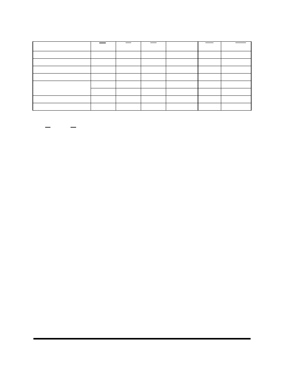
F
IGURE
1. R
EAD
T
IMING
W
AVEFORM
F
IGURE
2. D
WORD
W
RITE
T
IMING
W
AVEFORM
(1) (WE C
ONTROLLED
)
High
M
e
m
o
r
y
10
01.10.05 Rev 8
All data sheets are subject to change without notice
©2005 Maxwell Technologies
All rights reserved
Low Voltage 8 Megabit (256K x 32-Bit) EEPROM MCM
79LV0832
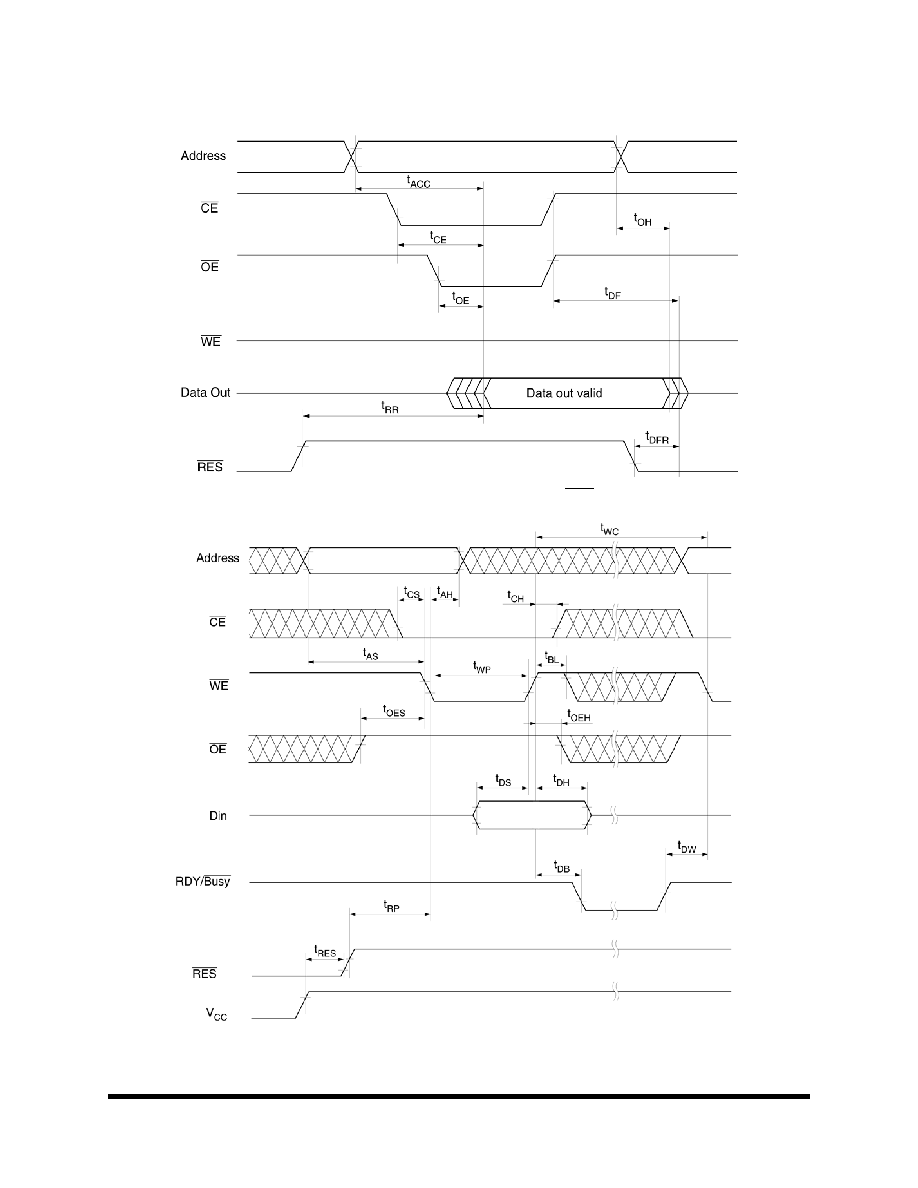
F
IGURE
3. D
WORD
W
RITE
T
IMING
W
AVEFORM
(2) (CE C
ONTROLLED
)
F
IGURE
4. P
AGE
W
RITE
T
IMING
W
AVEFORM
(1) (WE C
ONTROLLED
)
M
e
m
o
r
y
11
01.10.05 Rev 8
All data sheets are subject to change without notice
©2005 Maxwell Technologies
All rights reserved
Low Voltage 8 Megabit (256K x 32-Bit) EEPROM MCM
79LV0832
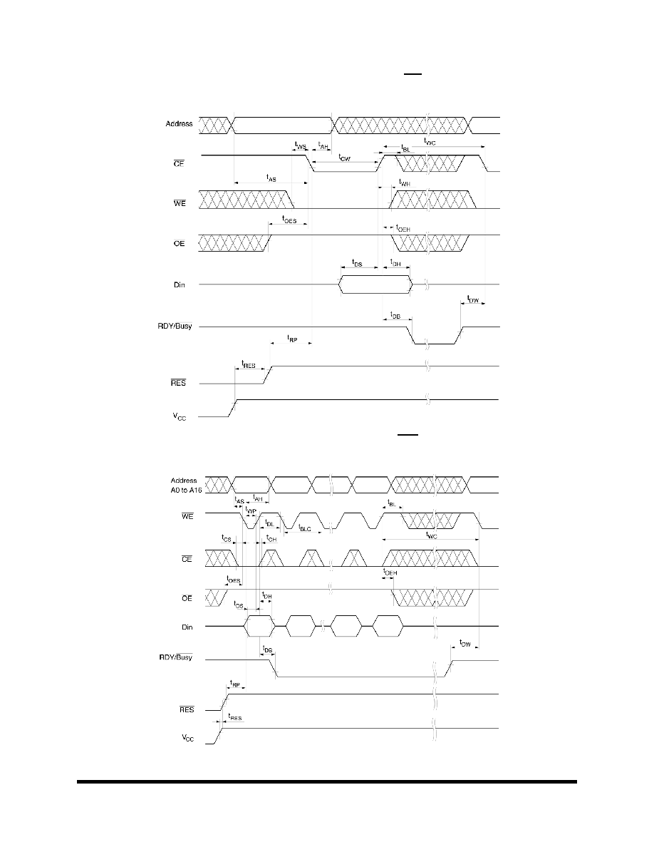
F
IGURE
5. P
AGE
W
RITE
T
IMING
W
AVEFORM
(2) (CE C
ONTROLLED
)
1,2
F
IGURE
6. D
ATA
P
OLLING
T
IMING
W
AVEFORM1
1) A7-A16
ARE
P
AGE
A
DDRESSES
AND
MUST
BE
THE
SAME
WITHIN
A
P
AGE
W
RITE
O
PERATION
2)
R
EFER
TO
T
ABLE
7
AND
8
FOR
TIMING
CHARACTERISTICS
I/O7, 15, 23, 31
1) R
EFER
TO
T
ABLE
7
AND
8
FOR
TIMING
CHARACTORISTICS

M
e
m
o
r
y
12
01.10.05 Rev 8
All data sheets are subject to change without notice
©2005 Maxwell Technologies
All rights reserved
Low Voltage 8 Megabit (256K x 32-Bit) EEPROM MCM
79LV0832
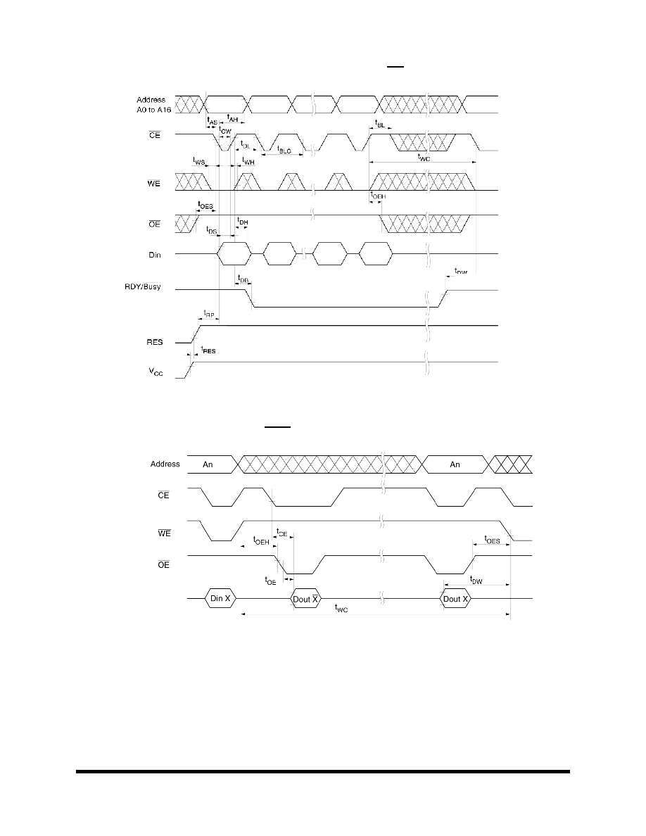
F
IGURE
7. S
OFTWARE
D
ATA
P
ROTECTION
T
IMING
W
AVEFORM
(1) (
IN
PROTECTION
MODE
)
1
F
IGURE
8. S
OFTWARE
D
ATA
P
ROTECTION
W
AVEFORM
(2) (
IN
NON
-
PROTECTION
MODE
)
1
EEPROM A
PPLICATION
N
OTES
This application note describes the programming procedures for the EEPROM modules and with details of various
techniques to preserve data integrity.
Automatic Page Write
Page-mode write feature allows 1 to 128 dwords of data to be written into the EEPROM in a single write cycle. Loading
the first dword of data, the data load window opens 30µ s for the second dword. In the same manner each additional
dword of data can be loaded within 30µ s of the preceding falling edge of either WE or CE. When CE and WE are kept
1)R
EPEAT
THE
DATA
PATTERN
IN
EACH
OF
THE
FOUR
BYTES
.
1) R
EPEAT
THE
DATA
PATTERN
IN
EACH
OF
THE
FOUR
BYTES
.
M
e
m
o
r
y
13
01.10.05 Rev 8
All data sheets are subject to change without notice
©2005 Maxwell Technologies
All rights reserved
Low Voltage 8 Megabit (256K x 32-Bit) EEPROM MCM
79LV0832
high for 100µ s after data input, the EEPROM enters the write mode automatically and the data input is written into the
EEPROM.
WE, CE Pin Operation
During a write cycle, addresses are latched by the falling edge of WE or CE, and data is latched by the rising edge of
WE or CE.
Data Polling
Data Polling function allows the status of the EEPROM to be determined. If EEPROM is set to read mode during a
write cycle, an inversion of the last dword of data to be loaded outputs from I/O 7, 15, 23, 31 to indicate that the
EEPROM is performing a write operation.
RDY/Busy Signal
RDY/Busy signal also allows a comparison operation to determine the status of the EEPROM. The RDY/Busy signal
goes low (V
OL)
after the first write signal. At the end of the write cycle, the RDY/Busy returns to a high state ( V
OH
).
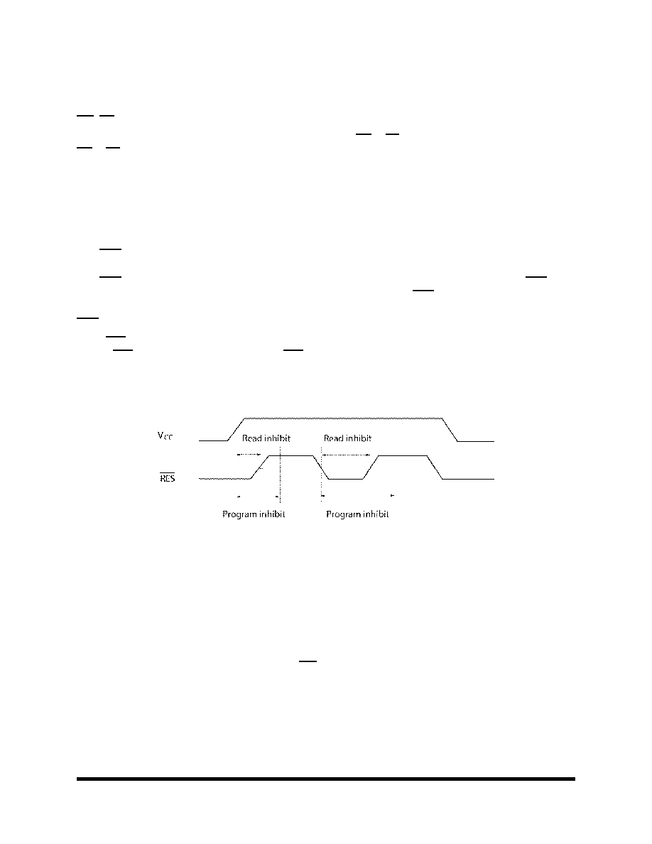
RES Signal
When RES is LOW (V
L
), the EEPROM cannot be read or programmed. The EEPROM data must be protected by
keeping RES low when V
CC
is power on and off. RES should be high (V
H
) during read and programming operations.
Data Protection
To protect the data during operation and power on/off, the EEPROM has the internal functions described below.
1. Data Protection at V
CC
on/off
When V
CC
is turned on or off, noise on the control pins generated by external circuits, such as CPUs, may turn the EEPROM to
programming mode by mistake. To prevent this unintentional programming, the EEPROM must be kept in an unprogrammable
state during V
CC
on/off by using a CPU reset signal to RES pin.
M
e
m
o
r
y
14
01.10.05 Rev 8
All data sheets are subject to change without notice
©2005 Maxwell Technologies
All rights reserved
Low Voltage 8 Megabit (256K x 32-Bit) EEPROM MCM
79LV0832
Data Protection
To protect the data during operation and power on/off, the EEPROM has the internal functions described below.
1. Data Protection against Noise of Control Pins (CE, OE, WE) during Operation.
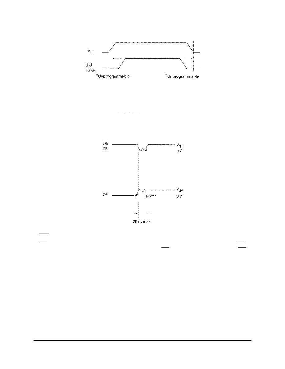
During readout or standby, noise on the control pins may act as a trigger and turn the EEPROM to programming mode by mis-
take. To prevent this phenomenon, the EEPROM has a noise cancellation function that cuts noise if its width is 20ns or less in
programming mode. Be careful not to allow noise of a width of more than 20ns on the control pins.
2. RES Signal
RES should be kept at V
SS
level when V
CC
is turned on or off. The EEPROM breaks off programming operation when RES
become low, programming operation doesn't finish correctly in case that RES falls low during programming operation. RES
should be kept high for 10 ms after the last data is input

M
e
m
o
r
y
15
01.10.05 Rev 8
All data sheets are subject to change without notice
©2005 Maxwell Technologies
All rights reserved
Low Voltage 8 Megabit (256K x 32-Bit) EEPROM MCM
79LV0832
.
3. Software Data Protection
Enable
The 79LV0832 contains a software controlled write protection feature that allows the user to inhibit all write operations to the
device. This is useful in protecting the device from unwanted write cycles due to uncontrollable circuit noise or inadvertent
writes caused by minor bus contentions. Software data protection is enabled by writing the following data sequence to the
EEPROM and allowing the write cycle period (t
WC
) of 10ms to elapse:
.
Software Data Protection Enable Sequence
4. Writing to the Memory with Software Data Protection Enabled
To write to the device once Software protection is enabled, the enable sequence must precede the data to be written. This
sequence allows the write to occur while at the same time keeping the software protection enabled
Sequence for Writing Data with Software Protection Enabled
.
15mS
Address
5555
AAAA or 2AAA
5555
Data
AA AA AA AA
55 55 55 55
A0 A0 A0 A0
Address
5555
AAAA or 2AAA
5555
Data
AA AA AA AA
55 55 55 55
A0 A0 A0 A0
Write Address(s)
Normal Data Input

M
e
m
o
r
y
16
01.10.05 Rev 8
All data sheets are subject to change without notice
©2005 Maxwell Technologies
All rights reserved
Low Voltage 8 Megabit (256K x 32-Bit) EEPROM MCM
79LV0832
5. Disabling Software Protection
Software data protection mode can be disabled by inputting the following data sequence. Once the software pro-
tection sequence has been written, no data can be written to the memory until the write cycle (T
WC
) has elapsed.
Software Protection Disable Sequence
Devices are shipped in the "unprotected" state, meaning that the contents of the memory can be changed as required
by the user. After the software data protection is enabled, the device enters the Protect Mode where no further write
commands have any effect on the memory contents.
Address
5555
AAAA or 2AAA
5555
Data
AAAA or 2AAA
55 55 55 55
20 20 20 20
5555
AA AA AA AA
80 80 80 80
55 55 55 55
AA AA AA AA
5555
M
e
m
o
r
y
17
01.10.05 Rev 8
All data sheets are subject to change without notice
©2005 Maxwell Technologies
All rights reserved
Low Voltage 8 Megabit (256K x 32-Bit) EEPROM MCM
79LV0832
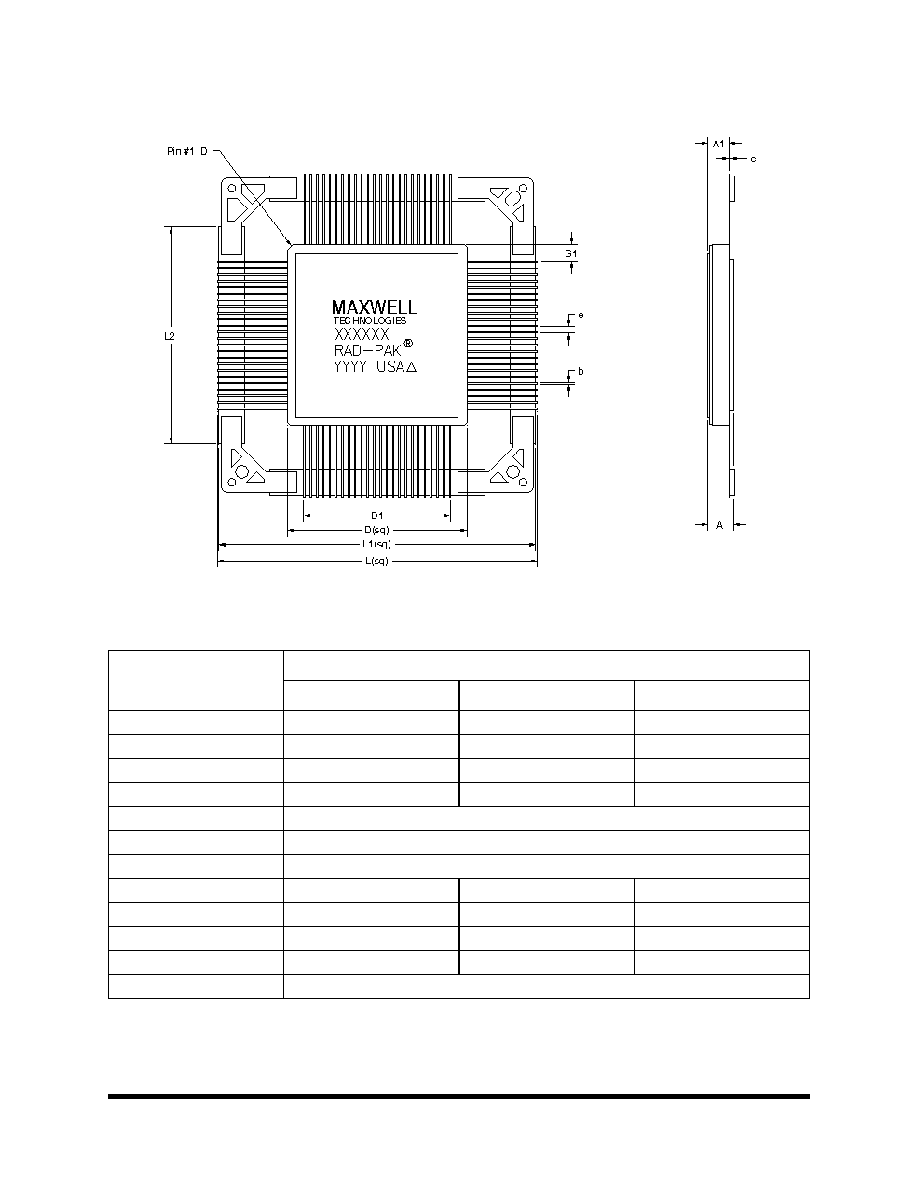
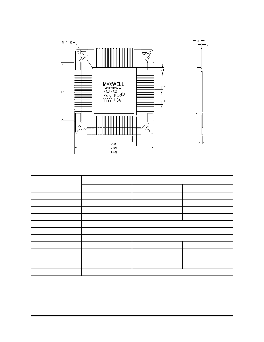
Note: All dimensions in inches
96-P
IN
R
AD
-P
AK
Æ Q
UAD
F
LAT
P
ACKAGE
S
YMBOL
D
IMENSION
M
IN
N
OM
M
AX
A
.184
.200
.216
b
.010
.012
.013
c
---
.009
.012
D
1.408
1.420
1.432
D1
1.162
e
.050
S1
.129
L
---
2.528
2.543
L1
2.485
2.500
2.505
L2
---
1.700
A1
.152
.165
.178
N
96
M
e
m
o
r
y
18
01.10.05 Rev 8
All data sheets are subject to change without notice
©2005 Maxwell Technologies
All rights reserved
Low Voltage 8 Megabit (256K x 32-Bit) EEPROM MCM
79LV0832
96 P
IN
R
AD
-T
OLERANT
Q
UAD
F
LAT
P
ACKAGE
Note: All dimensions in inches
S
YMBOL
D
IMENSION
M
IN
N
OM
M
AX
A
.167
.183
.199
b
.010
.012
.013
c
--
.009
.012
D
1.408
1.420
1.432
D1
1.162
e
.050
S1
.129
L
--
2.528
2.543
L1
2.485
2.500
2.505
L2
--
1.700
--
A1
.152
.165
.178
N
96
A
A1
c
L1(sq)
L(sq)
D(sq)
D1
L2
Pin #1 ID
S1
MAXWELL
TECHNOLOGIES
b
e
M
e
m
o
r
y
19
01.10.05 Rev 8
All data sheets are subject to change without notice
©2005 Maxwell Technologies
All rights reserved
Low Voltage 8 Megabit (256K x 32-Bit) EEPROM MCM
79LV0832
96 P
IN
X
RAY
Q
UAD
F
LAT
P
ACKAGE
Note: All dimensions in inches
S
YMBOL
D
IMENSION
M
IN
N
OM
M
AX
A
.200
.222
.245
b
.007
.010
.013
c
.009
.009
.012
D
1.690
1.707
1.725
D1
1.150
e
0.050
S1
.278
L
3.000
3.020
3.040
L1
2.985
3.000
3.005
L2
2.090
2.200
2.210
A1
.115
.130
.145
N
96

M
e
m
o
r
y
20
01.10.05 Rev 8
All data sheets are subject to change without notice
©2005 Maxwell Technologies
All rights reserved
Low Voltage 8 Megabit (256K x 32-Bit) EEPROM MCM
79LV0832
Important Notice:
These data sheets are created using the chip manufacturers published specifications. Maxwell Technologies verifies
functionality by testing key parameters either by 100% testing, sample testing or characterization.
The specifications presented within these data sheets represent the latest and most accurate information available to
date. However, these specifications are subject to change without notice and Maxwell Technologies assumes no
responsibility for the use of this information.
Maxwell Technologies' products are not authorized for use as critical components in life support devices or systems
without express written approval from Maxwell Technologies.
Any claim against Maxwell Technologies must be made within 90 days from the date of shipment from Maxwell Tech-
nologies. Maxwell Technologies' liability shall be limited to replacement of defective parts.
M
e
m
o
r
y
21
01.10.05 Rev 8
All data sheets are subject to change without notice
©2005 Maxwell Technologies
All rights reserved
Low Voltage 8 Megabit (256K x 32-Bit) EEPROM MCM
79LV0832
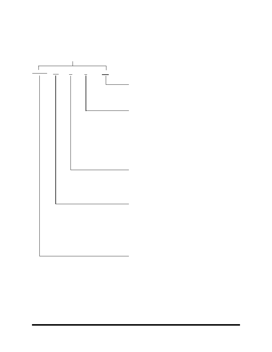
Product Ordering Options
1) Products are manufactured and screened to Maxwell Technologies self-defined Class H and Class K flows.
Model Number
Feature
Option Details
79LV0832
XX
Q
X
-XX
Access Time
Screening Flow
Package
Radiation Feature
Base Product
Nomenclature
20 = 200 ns
25 = 250 ns
Multi Chip Module (MCM)
1
K = Maxwell Self-Defined Class K
H = Maxwell Self-Defined Class H
I = Industrial (testing @ -55∞C,
+25∞C, +125∞C)
E = Engineering (testing @ +25∞C)
Q = Quad Flat Pack
RP = R
AD
-P
AK
Æ Package
XP = X
RAY
-P
AK
Package
RT1 = Guaranteed to 10 krad at
die level
RT2 = Guaranteed to 25 krad at
die level
RT4 = Guaranteed to 40 krad at
8 Megabit (256K x 32-Bit)
Low Voltage EEPROM MCM