 | –≠–ª–µ–∫—Ç—Ä–æ–Ω–Ω—ã–π –∫–æ–º–ø–æ–Ω–µ–Ω—Ç: 7B991 | –°–∫–∞—á–∞—Ç—å:  PDF PDF  ZIP ZIP |

1
Memory
All data sheets are subject to change without notice
(858) 503-3300 - Fax: (858) 503-3301 - www.maxwell.com
Programmable Skew
7B991
©2002 Maxwell Technologies.
All rights reserved.
Clock Buffer (PSCB)
09.23.02 Rev 4
F
EATURES
:
∑ All output pair skew < 100 ps typical (250 max.)
∑ 3.75 to 80 MHz output operation
∑ User-selectable output functions
∑ Selectable skew to 18 ns
∑ Inverted and non-inverted
∑ Operation at Ω and º input frequency
∑ Operation at 2x and 4x input frequency (input as low as
3.75 MHz)
∑ Zero input to output delay
∑ 50% duty-cycle outputs
∑ Outputs drive 50
terminated lines
∑ Low operating current
∑ Package: 32-pin R
AD
-P
AK
Æ flat package
∑ Jitter < 200 ps peak-to-peak (< 25 ps RMS)
∑ Compatible with PentiumTM-based processor
∑ Total dose hardness:
- >100 krads (Si), depending upon space mission
∑ Excellent Single Event Effects:
- SEL > 116MeV/mg/cm
2
- SEU
TH
-3 MeV/mg/cm
2
- SEU sat cross section: 1E-3/device
D
ESCRIPTION
:
Maxwell Technologies' 7B991 Programmable Skew Clock
Buffers (PSCB) offer user-selectable control over system
clock functions. These multiple-output clock drivers provide
the system integrator with functions necessary to optimize tim-
ing of high-performance computer systems. Eight individual
drivers, arranged as four pairs of user-controllable outputs,
can each drive terminated transmission lines with impedances
as low as 50
while delivering minimal and specified output
skews and full-swing logic levels.
Each output can be hardwired to one of nine delay or function
configurations. Delay increments of 0.7 to 1.5 ns are deter-
mined by the operating frequency with outputs able to skew up
to ± 6 time units from their nominal "zero" skew position. The
completely integrated PLL allows external load and transmis-
sion line delay effects to be canceled. When this "zero delay"
capability of the PSCB is combined with the selectable output
skew functions, the user can create output-to-output delays of
up to ±12 time units.
Maxwell Technologies' patented R
AD
-P
AK
Æ packaging technol-
ogy incorporates radiation shielding in the microcircuit pack-
age. It eliminates the need for box shielding while providing
the required radiation shielding for a lifetime in orbit or space
mission. In a GEO orbit, R
AD
-P
AK
provides greater than 100
krad (Si) radiation dose tolerance. This product is available
with screening up to Class S.
Logic Diagram

Memory
2
All data sheets are subject to change without notice
©2002 Maxwell Technologies.
All rights reserved.
Programmable Skew Clock Buffer (PSCB)
7B991
09.23.02 Rev 4
T
ABLE
1. 7B991 P
INOUT
D
ESCRIPTIONS
P
IN
S
YMBOL
I/O
D
ESCRIPTION
1
REF
I
Reference frequency input supplies the frequency and timing
against which all functional variation is measured.
17
FB
I
PLL feedback (typically connected to one of the eight outputs)
3
FS
I
Three-level frequency range select. See Table 2.
26, 27
1F0, 1F1
I
Three-level function select inputs for output pair 1 (1Q0, 1Q1). See
Table 2.
29, 30
2F0, 2F1
I
Three-level function select inputs for output pair 2 (2Q0, 2Q1). See
Table 2.
4, 5
3F0, 3F1
I
Three-level function select inputs for output pair 3 (3Q0, 3Q1). See
Table 2.
6, 7
4F0, 4F1
I
Three-level function select inputs for output pair 4 (4Q0, 4Q1). See
Table 2.
31
TEST
I
Three-level select. See test mode section under the block diagram
descriptions.
23, 24
1Q1, 1Q0
O
Output pair 1. See Table 2.
21, 22
2Q1, 2Q0
O
Output pair 2. See Table 2.
14, 15
3Q1, 3Q0
O
Output pair 3. See Table 2.
10, 11
4Q1, 4Q0
O
Output pair 4. See Table 2.
9, 16, 18, 25
V
CCN
PWR
Power supply for output drivers
2
V
CCQ
PWR
Power supply for internal circuitry
12, 13, 21,
22, 28, 32
GND
PWR
Ground.
T
ABLE
2. 7B991 A
BSOLUTE
M
AXIMUM
R
ATINGS
P
ARAMETER
S
YMBOL
M
IN
M
AX
U
NIT
Storage Temperature
T
S
-65
150
∞C
Operating Temperature Range
T
A
-40
85
∞C
Supply Voltage to Ground Potential
V
S
-0.5
7.0
V
DC Input Voltage
V
I
-0.5
7.0
V
Output Current into Outputs (LOW)
I
OUT
--
64
mA
Static Discharge Voltage (per MIL-STD-882, Method 3015)
V
SD
>2001
--
V
Latchup Current
I
LU
>200
--
mA
Memory
3
All data sheets are subject to change without notice
©2002 Maxwell Technologies.
All rights reserved.
Programmable Skew Clock Buffer (PSCB)
7B991
09.23.02 Rev 4
T
ABLE
3. D
ELTA
L
IMITS
P
ARAMETER
V
ARIATION
I
CCQ
±10% of specified value in Table 5
I
CCN
±10% of specified value in Table 5
T
ABLE
4. 7B991 R
ECOMMENDED
O
PERATING
C
ONDITIONS
P
ARAMETER
S
YMBOL
M
IN
M
AX
U
NIT
Supply Voltage
V
CC
-0.5
+7.0
V
Input HIGH Voltage (REF and FB
inputs only)
V
IH
2.0
V
CC
V
Input LOW Voltage (REF and FB
inputs only)
V
IL
-0.5
0.8
V
Three-Level Input HIGH Voltage (Test,
FS, xFn)
1
1. These inputs are normally wired to V
CC
,GND, or left unconnected (actual threshold voltages vary as a percentage of V
CC
).
Internal termination resistors hold unconnected inputs at V
CC
/2. If these inputs are switched, the function and timing of the out-
puts may glitch and the PLL may require an additional t
LOCK
time before all datasheet limits are achieved.
V
IHH
V
CC
-0.85
V
CC
V
Thermal Impedance
JC
--
3.43
∞C/W
T
ABLE
5. 7B991 DC E
LECTRICAL
C
HARACTERISTICS
(V
CC
= 5V ±10%, T
A
= -40
TO
85∞C,
UNLESS
OTHERWISE
SPECIFIED
)
P
ARAMETER
S
YMBOL
T
EST
C
ONDITIONS
S
UBGROUPS
M
IN
M
AX
U
NIT
Output HIGH Voltage
V
OH
V
CC
= Min, I
OH
= -16 mA
1, 2, 3
2.4
--
V
Output LOW Voltage
V
OL
V
CC
= Min, I
OL
= 46 mA
1, 2, 3
--
0.45
V
Input HIGH Voltage (REF and FB
inputs only)
V
IH
1, 2, 3
2.0
--
V
Input LOW Voltage (REF and FB
inputs only)
V
IL
1, 2, 3
--
0.8
V
Three-Level Input HIGH Voltage
(Test, FS, xFn)
1
V
IHH
Min < V
CC
< Max
1, 2, 3
V
CC
-0.85
--
V
Three-Level Input MID Voltage
(Test, FS, xFn)
1
V
IMM
Min < V
CC
< Max
1, 2, 3
V
CC
/2 -
500 mV
V
CC
/2 +
500 mV
V
Three-Level Input LOW Voltage
(Test, FS, xFn)
1
V
ILL
Min < V
CC
< Max
1, 2, 3
0.0
0.85
V
Input HIGH Leakage Current
(REF and FB inputs only)
I
IH
V
CC
= Max, V
IN
= 5V
1, 2, 3
--
10
µ A
Input LOW Leakage Current
(REF and FB inputs only)
I
IL
V
CC
= Max, V
IN
= 0.4V
1, 2, 3
-500
--
µ A

Memory
4
All data sheets are subject to change without notice
©2002 Maxwell Technologies.
All rights reserved.
Programmable Skew Clock Buffer (PSCB)
7B991
09.23.02 Rev 4
Input HIGH Current (Test, FS, xFn)
I
IH
V
IN
= V
CC
1, 2, 3
--
200
µ A
Input MID Current (Test, FS, xFn)
I
IMM
V
IN
= 2.75
1, 2, 3
-200
200
µ A
Input LOW Current (Test, FS, xFn)
I
ILL
V
IN
= GND
1, 2, 3
--
-200
µ A
Output Short Circuit (Test, FS, xFn)
2
I
OS
V
CC
= Max., V
OUT
= GND
(25
∞
C only)
1
--
-250
mA
Operating Current used by Internal
Circuitry
I
CCQ
V
CCN
= V
CCQ
= Max, all input
selects open
1, 2, 3
--
90
mA
Output Buffer Current per Output
Pair
3
I
CCN
V
CCN
= V
CCQ
= Max,
I
OUT
= 0 mA,
Input selects open, fMAX
1, 2, 3
--
14
mA
Power Dissipation per Output Pair
4
P
D
V
CCN
= V
CCQ
= Max,
I
OUT
= 0 mA
Input selects open, fMAX
1, 2, 3
--
78
mW
1. These inputs are normally wired to V
CC
,GND, or left unconnected (actual threshold voltages vary as a percentage of V
CC
). Inter-
nal termination resistors hold unconnected inputs at V
CC
/2. If these inputs are switched, the function and timing of the outputs
may glitch and the PLL may require an additional t
LOCK
time before all datasheet limits are achieved.
2. This device should be tested one output at a time, output shorted for less than one second, less than 10% duty cycle. Room
temperature only.
3. Total output current per output pair can be approximated by the following expression that includes device current plus load cur-
rent:
ICCN = [(4 + 0.11F) + [((835-3F)/Z) + (.0022FC)]N] x 1.1
Where:
f = frequency in MHz
C = capacitive load in pF
Z = line impedance in ohms
N = number of loaded outputs; 0, 1, or 2
FC = F * C
4. Total power dissipation per output pair can be approximated by the following expression that includes device power dissipation
due to the load circuit:
PD = [(22 + 0.61F) + [((1550-2.7F)/Z) + (.0125FC)]N] x 1.1
T
ABLE
6. 7B991 C
APACITANCE1
1. Guaranteed by design.
P
ARAMETER
S
YMBOL
T
EST
C
ONDITIONS
M
AX
U
NIT
Input Capacitance
C
IN
T
A
= 25
∞
C, f = 1 MHz, V
CC
= 5.0V
10
pF
T
ABLE
5. 7B991 DC E
LECTRICAL
C
HARACTERISTICS
(V
CC
= 5V ±10%, T
A
= -40
TO
85∞C,
UNLESS
OTHERWISE
SPECIFIED
)
P
ARAMETER
S
YMBOL
T
EST
C
ONDITIONS
S
UBGROUPS
M
IN
M
AX
U
NIT

Memory
5
All data sheets are subject to change without notice
©2002 Maxwell Technologies.
All rights reserved.
Programmable Skew Clock Buffer (PSCB)
7B991
09.23.02 Rev 4
F
IGURE
1. TTL AC T
EST
L
OAD
F
IGURE
2. TTL I
NPUT
T
EST
W
AVEFORM
T
ABLE
7. AC E
LECTRICAL
C
HARACTERISTICS
1,2,3
(V
CC
= 5V ±10%, T
A
= -40
TO
85∞C,
UNLESS
OTHERWISE
SPECIFIED
)
P
ARAMETER
S
YMBOL
S
UBGROUPS
M
IN
T
YP
M
AX
U
NIT
Operating Clock Frequency in MHz
FS = LOW
1,4
f
NOM
9, 10, 11
15
--
30
MHz
FS = MID
1,4
25
--
50
FS = HIGH
1,4,5
40
--
80
REF Pulse Width HIGH
t
RPWH
9, 10, 11
5.0
--
--
ns
REF Pulse Width LOW
t
RPWL
9, 10, 11
5.0
--
--
ns
Programmable Skew Unit
t
U
9, 10, 11
See Table 2
Zero Output Matched-Pair Skew (XQ0, XQ1)
6,7
t
SKEWPR
9, 10, 11
--
0.1
0.50
ns
Zero Output Skew (All Outputs)
6,8,9
t
SKEW0
9, 10, 11
--
0.3
0.75
ns
Output Skew (Rise-Rise, Fall-Fall, Same Class Out-
puts)
6,10
t
SKEW1
9, 10, 11
--
0.6
1.0
ns
Output Skew (Rise-Fall, Nominal-Inverted, Divided-
Divided)
6,10
t
SKEW2
9, 10, 11
--
1.0
1.5
ns
Output Skew (Rise-Rise, Fall-Fall, Different Class
Outputs)
6,10
t
SKEW3
9, 10, 11
--
0.7
1.2
ns
Output Skew (Rise-Fall, Nominal-Divided, Divided-
Inverted)
6,10
t
SKEW4
9, 10, 11
--
1.2
1.7
ns
Device-to-Device Skew
1,11,12
t
DEV
9, 10, 11
--
--
1.65
ns
Propagation Delay, REF Rise to FB Rise
t
PD
9, 10, 11
-1
0.0
1
ns
Output Duty Cycle Variation
13
t
ODCV
9, 10, 11
-1.2
0.0
1.2
ns

Memory
6
All data sheets are subject to change without notice
©2002 Maxwell Technologies.
All rights reserved.
Programmable Skew Clock Buffer (PSCB)
7B991
09.23.02 Rev 4
Output HIGH Time Deviation from 50%
14,15
t
PWH
9, 10, 11
--
--
3
ns
Output LOW Time Deviation from 50%
14,15
t
PWL
9, 10, 11
--
--
3.5
ns
Output Rise Time
14,16
t
ORISE
9, 10, 11
0.15
1.5
2.5
ns
Output Fall Time
14,16
t
OFALL
9, 10, 11
0.15
1.5
2.5
ns
PLL Lock Time
17
t
LOCK
9, 10, 11
--
--
0.5
ms
Cycle-to-Cycle Output Jitter
Peak-to-
Peak
3
t
JR
9, 10, 11
--
--
200
ps
1. The level to be set of FS in determined by the "normal" operating frequency (f
NOM
) of the V
CO
and Time Unit Generator (see
Logic Block Diagram). Nominal frequency (f
NOM
) always appears at 1Q0 and the other outputs when they are operated in their
undivided modes (See Table 9). The frequency appearing at the REF and FB inputs will be f
NOM
when the output connected to
FB is undivided. The frequency of the REF and FB inputs will be f
NOM
/2 or f
NOM
/4 when the part is configured for a frequency
multiplication by using a divided output as the FB input.
2. Test measurement levels for the 7B991 are TTL levels (1.5V to 1.5V). Test conditions assume signal transition times of 2 ns or
less and output loading as shown in the AC Test Loads and Waveforms unless otherwise specified.
3. Guaranteed by statistical correlation. Tested initially and after any design or process changes that may affect these parameters.
4. For all three state inputs. HIGH indicates a connection to V
CC
, LOW indicates a connection to GND, and MID indicates an open
connections. Internal termination circuitry holds an unconnected input to V
CC
/2.
5. When the FS pin is selected HIGH, the REF input must not transition upon power-up until V
CC
has reached 4.3V.
6. SKEW is defined as the time between the earliest and the latest output transition among all outputs for which the same t
U
delay
has been selected when all are loaded with 50 pF and terminated with 50
to 2.06V.
7. t
SKEWPR
is defined as the skew between a pair of outputs (XQ0 and XQ1) when all eight outputs are selected for 0t
U
.
8. t
SKEW0
is defined as the skew between outputs when they are selected for 0t
U
. Other outputs are divided or inverted but not
shifted.
9. C
L
= 0 pF. For C
L
= 30 pF, t
SKEW0
= 0.35 ns.
10.There are three classes of outputs: Nominal (multiple of t
U
delay), Inverted (4Q0 and 4Q1 only with 4F0 = 4F1 = HIGH), and
divided (3Qx and 4Qx only in Divide-by-2 or Divide-by-4 mode).
11. t
DEV
is the output-to-output skew between any two devices operating under the same conditions (V
CC
ambient temperature, air
flow, etc.)
12.Guaranteed by design.
13.t
ODCV
is the deviation of the output from a 50% duty cycle. Output pulse width variations are included in t
SKEW2
and t
SKEW4
spec-
ifications.
14.Specified with outputs loaded 30 pF for the 7B99 devices. Devices are terminated through 50
to 2.05V.
15.t
PWH
is measured at 2.0V. t
PWL
is measured at 0.8V.
16.t
ORISE
and t
OFALL
measured between 0.8V and 2.0V.
17.t
LOCK
is the time that is required before synchronization is achieved. This specification is valid only after V
CC
is stable and within
normal operating limits. This parameter is measured from the application of a new signal or frequency at REF or FB until t
PD
is
within specified limits.
T
ABLE
7. AC E
LECTRICAL
C
HARACTERISTICS
1,2,3
(V
CC
= 5V ±10%, T
A
= -40
TO
85∞C,
UNLESS
OTHERWISE
SPECIFIED
)
P
ARAMETER
S
YMBOL
S
UBGROUPS
M
IN
T
YP
M
AX
U
NIT
Memory
7
All data sheets are subject to change without notice
©2002 Maxwell Technologies.
All rights reserved.
Programmable Skew Clock Buffer (PSCB)
7B991
09.23.02 Rev 4
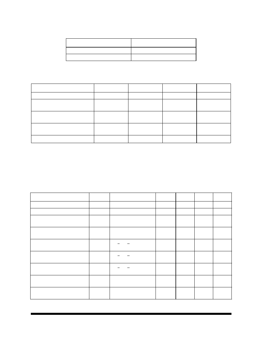
F
IGURE
3. AC T
IMING
D
IAGRAMS

Memory
8
All data sheets are subject to change without notice
©2002 Maxwell Technologies.
All rights reserved.
Programmable Skew Clock Buffer (PSCB)
7B991
09.23.02 Rev 4
B
LOCK
D
IAGRAM
D
ESCRIPTION
Phase Frequency Detector and Filter
These two blocks accept inputs from the reference frequency (REF) input and the feedback (FB) input and generate
correction information to control the frequency of the Voltage-Controlled Oscillator (VCO). These blocks, along with
the VCO, form a Phase-Locked Loop (PLL) that tracks the incoming REF signal.
VCO and Time Unit Generator
The VCO accepts analog control inputs from the PLL filter block and generates a frequency that is used by the time
unit generator to create discrete time units that are selected in the skew select matrix. The operational range of the
VCO is determined by the FS control pin. The time unit (t
U
) is determined by the operating frequency of the device and
the level of the FS pin as shown in Table 1.
Skew Select Matrix
The skew select matrix is comprised of four independent sections. Each section has two low-skew, high-fanout driv-
ers(xQ0, xQ1), and two corresponding three-level function select (xF0, xF1) inputs. Table 9 below shows the nine pos-
sible output functions for each section as determined by the function select inputs. All times are measured with respect
to the REF input assuming that the output connected to the FB input has 0t
U
selected.
T
ABLE
8. 7B991 F
REQUENCY
R
ANGE
S
ELECT
AND
t
U
C
ALCULATION1
1. For all three state inputs. HIGH indicates a connection to V
CC
. LOW indicates a connection to GND, and MID indicates an
open connection. Internal termination circuitry holds an unconnected input to V
CC
/2.
FS
2,3
2. The level to be set of FS is determined by the "normal" operating frequency (f
NOM
) of the V
CO
and Time Unit Generator (see
Logic Block Diagram). Nominal frequency (f
NOM
) always appears at 1Q0 and the other outputs when they are operated in their
undivided modes (See Table 9). The frequency appearing at the REF and FB inputs will be f
NOM
when the output connected to
FB is undivided. The frequency appearing at the REF and FB inputs will be f
NOM
/2 or f
NOM
/4 when the part is configured for a
frequency multiplication by using a divided output as the FB input.
3. When the FS pin is selected HIGH, the REF input must not transition upon power-up until V
CC
has reached 4.3V.
fNOM (MH
Z
)
t
U
= 1/fNOM
X
N
WHERE
N =
A
PPROXIMATE
F
REQUENCY
(MH
Z
)
AT
WHICH
t
U
= 1.0 ns
M
IN
M
AX
LOW
15
30
44
22.7
MID
25
50
26
38.5
HIGH
40
80
16
62.5
Memory
9
All data sheets are subject to change without notice
©2002 Maxwell Technologies.
All rights reserved.
Programmable Skew Clock Buffer (PSCB)
7B991
09.23.02 Rev 4
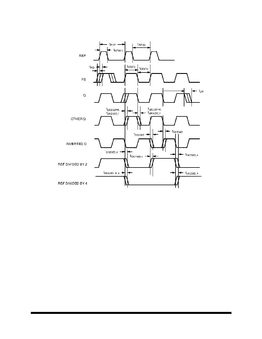
F
IGURE
4. T
YPICAL
O
UTPUTS
WITH
FB C
ONNECTED
TO
A
Z
ERO
-S
KEW
O
UTPUT1
1. FB connected to an output selected for "zero" skew (i.e. xF1 = xF0 = MID)
T
ABLE
9. 7B991 P
ROGRAMMABLE
S
KEW
C
ONFIGURATIONS
1
1. For all three state inputs. HIGH indicates a connection to V
CC
. LOW indicates a connection to GND, and MID indicates an open
connections. Internal termination circuitry holds an inconnected input to V
CC
/2.
F
UNCTION
S
ELECTS
O
UTPUT
F
UNCTIONS
1F1, 2F1, 3F1, 4F1
1F0, 2F0, 3F0, 4F0
1Q0, 1Q1, 2Q0, 2Q1
3Q0, 3Q1
4Q0, 4Q1
LOW
LOW
-4t
U
Divide by 2
Divide by 2
LOW
MID
-3t
U
-6t
U
-6t
U
LOW
HIGH
-2t
U
-4t
U
-4t
U
MID
LOW
-1t
U
-2t
U
-2t
U
MID
MID
0t
U
0t
U
0t
U
MID
HIGH
+1t
U
+2t
U
+2t
U
HIGH
LOW
+2t
U
+4t
U
+4t
U
HIGH
MID
+3t
U
+6t
U
+6t
U
HIGH
HIGH
+4t
U
Divide by 4
Inverted

Memory
10
All data sheets are subject to change without notice
©2002 Maxwell Technologies.
All rights reserved.
Programmable Skew Clock Buffer (PSCB)
7B991
09.23.02 Rev 4
Test Mode
The TEST input is a three-level input. In normal system operation, this pin is connected to ground, allowing the
7B991RP to operate as explained briefly above (for testing purposes, any of the three-level inputs can have a remov-
able jumper to ground, or be tied LOW through a 100
resistor. This will allow an external tester to change the state
of these pins.)
If the TEST input is forced to its MID or HIGH state, the device will operate with its internal phase locked loop discon-
nected, and input levels supplied to REF will directly control all outputs. Relative output to output functions are the
same as in normal mode.
In contrast with normal operation (TEST tied LOW). All outputs will function based only on the connection of their own
function select inputs (xF0 and xF1) and the waveform characteristics of the REF input.

Memory
11
All data sheets are subject to change without notice
©2002 Maxwell Technologies.
All rights reserved.
Programmable Skew Clock Buffer (PSCB)
7B991
09.23.02 Rev 4
O
PERATIONAL
M
ODE
D
ESCRIPTIONS
F
IGURE
5. Z
ERO
-S
KEW
AND
/
OR
Z
ERO
-D
ELAY
C
LOCK
D
RIVER
Figure 5 shows the PSCB configured as a zero-skew clock buffer. In this mode, the 7B991 can be used as the basis
for a low-skew clock distribution tree. When all of the function select inputs (xF0, xF1) are left open, the outputs are
aligned and may each drive a terminated transmission line to an independent load. The FB input can be tied to any
output in this configuration and the operating frequency range is selected with the FS pin. The low-skew specification,
coupled with the ability to drive terminated transmission lines (with impedances as low as 50
), allow efficient printed
circuit board design.
F
IGURE
6. P
ROGRAMMABLE
-S
KEW
C
LOCK
D
RIVE
Figure 6 shows a configuration to equalize skew between metal traces of different lengths. In addition to low skew
between outputs, the PSCB can be programmed to stagger the timing of its outputs. The four groups of output pairs
can each be programmed to different output timing. Skew timing can be adjusted over a wide range in small incre-
ments with the appropriate strapping of the function select pins. In this configuration, the 4Q0 output is fed back to FB
and configured for zero skew. The other three pairs of outputs are programmed to yield different skews relative to the
feedback. By advancing the clock signal on the longer traces or retarding the clock signal on shorter traces, all loads
can receive the clock pulse at the same time.
In this illustration, the FB input is connected to an output with 0-ns skew (xF1, xF0 = MID) selected. The internal PLL
synchronizes the FB and REF inputs and aligns their rising edges to insure that all outputs have precise phase align-
ment.

Memory
12
All data sheets are subject to change without notice
©2002 Maxwell Technologies.
All rights reserved.
Programmable Skew Clock Buffer (PSCB)
7B991
09.23.02 Rev 4
Clock skews can be advanced by ± 6 time units (t
U
) when using an output selected for zero skew as the feedback. A
wider range of delays is possible if the output connected to FB is also skewed. Since "Zero Skew", +t
U
and -t
U
are
defined relative to output groups, and since the PLL aligns the rising edges of REF and FB, it is possible to create
wider output skews by proper selection of the xFn inputs. For example, a +10 t
U
between REG and 3Qx can be
achieved by connecting 1Q0 to FB and setting 1F0 = 1F1 = GND, 3F0 = MID, and 3F1 = HIGH (Since FB aligns at -4
t
U
and 3Qx skews to +6 t
U
, a total of +10 t
U
skew is realized.). Many other configurations can be realized by skewing
both the output used as the FB input and skewing the other outputs.
F
IGURE
7. I
NVERTED
O
UTPUT
C
ONNECTIONS
Figure shows an example of the invert function of the PSCB. In this example the 4Q0 output used as the FB input is
programmed for invert (4F0 = 4F1 = HIGH) while the other three pairs of outputs are programmed for zero skew.
When 4F0 and 4F1 are tied high, 4Q0 and 4Q1 become inverted zero phase outputs. The PLL aligns the rising edge
of the FB input with the rising edge of the REF. This causes the 1Q, 2Q, and 3Q outputs to become the "inverted" out-
puts with respect to the REF input. By selecting which output connects to FB, it is possible to have 2 inverted and 6
non-inverted output or 6 inverted and 2 non-inverted outputs. The correct configuration would be determined by the
need for more (or fewer) inverted outputs. 1Q, 2Q, and 3Q outputs can also be skewed to compensate for varying
trace delays independent of inversion on 4Q.
F
IGURE
8. F
REQUENCY
M
ULTIPLIER
WITH
S
KEW
C
ONNECTIONS
Figure illustrates the PSCB configured as a clock multiplier. The 3Q0 output is programmed to divide by four and is
fed back to FB. This causes the PLL to increase its frequency until the 3Q0 and 3Q1 outputs are locked at 20 MHz
while the 1Qx and 2Qx outputs run at 80 MHz. The 4Q0 and 4Q1 outputs are programmed to divide by two, which

Memory
13
All data sheets are subject to change without notice
©2002 Maxwell Technologies.
All rights reserved.
Programmable Skew Clock Buffer (PSCB)
7B991
09.23.02 Rev 4
results in a 40 MHz waveform at these outputs. Note that the 20 and 40 MHz clocks fall simultaneously and are out of
phase on their rising edge. This will allow the designer to use the rising edges of the Ω frequency and º frequency
outputs without concern for rising-edge skew. The 2Q0, 2Q1, 1Q0, and 1Q1 outputs run at 80 MHz and are skewed by
programming their select inputs accordingly. Note that the FS pin is wired for 80 MHz operation because that is the fre-
quency of the fastest output.
F
IGURE
9. F
REQUENCY
D
IVIDER
C
ONNECTIONS
Figure demonstrates the PSCB in a clock divider application. 2Q0 is fed back to the FB input and programmed for
zero skew. 3Qx is programmed to divide by four. 4Qx is programmed to divide by two. Note that the falling edges of
the 4Qx and 3Qx outputs are aligned. This allows use of the rising edges of the Ω frequency and º frequency without
concern for skew mismatch. The 1Qx outputs are programmed to zero skew and are aligned with the 2Qx outputs. In
this example, the FS input is grounded to configure the device in the 15 to 30 MHz range since the highest frequency
output is running at 20 MHz.
F
IGURE
10. M
ULTI
-F
UNCTION
C
LOCK
D
RIVER
Figure shows some of the functions that are selectable on the 3Qx and 4Qx outputs. These include inverted outputs
and outputs that offer divide-by-2 and divide-by-4 timing. An inverted output allows the system designer to clock differ-
ent sub-systems on opposite edges, without suffering from the pulse asymmetry typical of non-ideal loading. This
function allows the two subsystems to each be clocked 180 degrees out of phase, but still to be aligned within the
skew specification.
The divided outputs offer a zero-delay divider for portions of the system that need the clock to be divided by either two
or four, and still remain within a narrow skew of the "1X" clock. Without this feature, an external divider would need to
be added, and the propagation delay of the divider would add to the skew between the different clock signals.

Memory
14
All data sheets are subject to change without notice
©2002 Maxwell Technologies.
All rights reserved.
Programmable Skew Clock Buffer (PSCB)
7B991
09.23.02 Rev 4
These divided outputs, coupled with the Phase Locked Loop, allow the PSCB to multiply the clock rate at the REF
input by either two or four. This mode will enable the designer to distribute a low-frequency clock between various por-
tions of the system, and then locally multiply the clock rate to a more suitable frequency, while still maintaining the low-
skew characteristics described above at the same time. It can multiply by two and four or divide by two (and four) at
the same time that it is shifting its outputs over a wide range or maintaining zero skew between selected outputs.
F
IGURE
11. B
OARD
-
TO
-B
OARD
C
LOCK
D
ISTRIBUTION
Figure shows the 7B991 connected in series to construct a zero-skew clock distribution tree between boards. Delays
of the downstream clock buffers can be programmed to compensate for the wire length (i.e. select negative skew
equal to the wire delay) necessary to connect them to the master clock source, approximating a zerp-delay clock tree.
Cascaded clock buffers will accumulate low-frequency jitter because of the non-ideal filtering characteristics of the
PLL filter. It is recommended that not more than two clock buffers be connected in series.

Memory
15
All data sheets are subject to change without notice
©2002 Maxwell Technologies.
All rights reserved.
Programmable Skew Clock Buffer (PSCB)
7B991
09.23.02 Rev 4
F32-01
Note: All dimensions in inches
32 P
IN
R
AD
-P
AK
Æ F
LAT
P
ACKAGE
S
YMBOL
D
IMENSION
M
IN
N
OM
M
AX
A
0.117
0.130
0.163
b
0.015
0.017
0.022
c
0.004
0.005
0.009
D
--
0.820
0.830
E
0.404
0.410
0.416
E1
--
--
0.440
E2
0.234
0.240
--
E3
0.030
0.085
--
e
0.050 BSC
L
0.350
0.370
0.390
Q
0.020
0.033
0.036
S1
0.005
0.027
--
N
32

Memory
16
All data sheets are subject to change without notice
©2002 Maxwell Technologies.
All rights reserved.
Programmable Skew Clock Buffer (PSCB)
7B991
09.23.02 Rev 4
Important Notice:
These data sheets are created using the chip manufacturer's published specifications. Maxwell Technologies verifies
functionality by testing key parameters either by 100% testing, sample testing or characterization.
The specifications presented within these data sheets represent the latest and most accurate information available to
date. However, these specifications are subject to change without notice and Maxwell Technologies assumes no
responsibility for the use of this information.
Maxwell Technologies' products are not authorized for use as critical components in life support devices or systems
without express written approval from Maxwell Technologies.
Any claim against Maxwell Technologies must be made within 90 days from the date of shipment from Maxwell Tech-
nologies. Maxwell Technologies' liability shall be limited to replacement of defective parts.

Memory
17
All data sheets are subject to change without notice
©2002 Maxwell Technologies.
All rights reserved.
Programmable Skew Clock Buffer (PSCB)
7B991
09.23.02 Rev 4
Product Ordering Options
Model Number
Feature
Option Details
7B991
XX
F
X
Screening Flow
Package
Radiation Feature
Base Product
Nomenclature
Monolithic
S = Maxwell Class S
B = Maxwell Class B
I = Industrial (testing @ -40∞C,
+25∞C, +85∞C)
E = Engineering (testing @ +25∞C)
F = Flat Pack
RP = R
AD
-P
AK
Æ package
Programmable Skew Clock Buffer
(PSCB)