 | –≠–ª–µ–∫—Ç—Ä–æ–Ω–Ω—ã–π –∫–æ–º–ø–æ–Ω–µ–Ω—Ç: 80387 | –°–∫–∞—á–∞—Ç—å:  PDF PDF  ZIP ZIP |

1
M
e
m
o
r
y
All data sheets are subject to change without notice
(858) 503-3300 - Fax: (858) 503-3301 - www.maxwell.com
Math Coprocessor
80387DX
©2002 Maxwell Technologies
All rights reserved.
05.07.02 REV 1
F
EATURES
:
∑ 80-Bit numeric processor
∑ R
AD
-P
AK
Æ radiation hardened against natural space radia-
tion
∑ Total dose hardness:
- > 100 krad (Si)
- dependant upon space mission
∑ Single Event Effects:
- SEU Threshold is ~ 3.38 MeV/mg/cm
2
- SEL Threshold = 37.1 - 59.9 MeV/mg/cm
2
∑ Package: 68-pin R
AD
-P
A
Æ quad flat pack
∑ Eight 80-bit numeric registers, usable as individual addres-
sable general registers or as a register stack
∑ Data types include:
- 32-, 64-, 80-bit floating point
- 32-, 64-bit integers
- 18-digit BCD operands
∑ 5 V Only power
∑ Built-in exception handling
∑ Upward object code compatible with All 80X87DX micro-
processors
∑ Full-range transcendental operations for SINE, COSINE,
TANGENT, ARCTANGENT and LOGARITHM
D
ESCRIPTION
:
Maxwell's 80387DX high speed microcircuit features a greater
than 100 kilorad (Si) total dose tolerance. Using Maxwell's
radiation hardened R
AD
-P
AK
Æ packaging technology, the
80387DX is a high-performance numerics processor that
extends the 80386DX architecture with floating point,
extended integer and BCD data types. The computing system
fully conforms to the ANSI/IEEE floating-point standard.
Using a numerics oriented architecture, the 80387DX adds
over seventy mnemonics to the 80386DX instruction set, mak-
ing the 80386DX/80387DX a complete solution for high-per-
formance numerics processing.
Maxwell Technologies' patented R
AD
-P
AK
packaging technol-
ogy incorporates radiation shielding in the microcircuit pack-
age. It eliminates the need for box shielding while providing
the required radiation shielding for a lifetime in orbit or space
mission. In a GEO orbit, R
AD
-P
AK
provides greater than 100
krad (Si) radiation dose tolerance. This product is available
with screening up to Class S.
Logic Diagram
Logic Diagram
80387

M
e
m
o
r
y
2
05.07.02 REV 1
All data sheets are subject to change without notice
©2002 Maxwell Technologies
All rights reserved.
Math Coprocessor
80387DX
T
ABLE
1. P
INOUT
D
ESCRIPTION
P
IN
S
YMBOL
D
ESCRIPTION
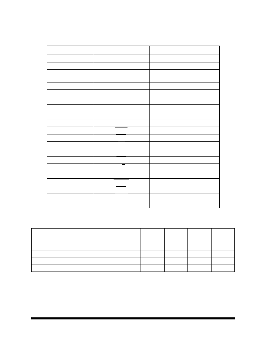
1, 12, 19, 21, 35, 49, 53, 56
V
SS
Ground
2, 13, 20, 32, 36, 39, 52, 68
V
CC
Positive Power Supply
3-11, 18, 22-31, 33, 34, 37,
38, 40, 41, 64-67
D4-D12, D15, D16-25, D26, D27,
D28, D29, D30, D31, D0-D3
Data Bus
42
CKM
Clock Mode
43
386CLK2
386 CPU Clock 2
44
387CLK2
387 MCP Clock 2
45
RESETIN
System Reset
46
NC
Not Connected
47 59
Tie High
Tie High
48
READY
Bus Ready Input
50
CMD0
Command
51
ADS
Address Strobe
54
NPS2
MCP Select #2
55
NPS1
MCP Select #1
57
W/R
Write/Read
58
STEN
Status Enable
60
READYO
Ready Output
61
BUSY
Busy Status
62
ERROR
Error Status
63
PEREQ
Processor Extension Request
T
ABLE
2. A
BSOLUTE
M
AXIMUM
R
ATINGS
P
ARAMETER
S
YMBOL
M
IN
M
AX
U
NIT
Voltage, any pin, with respect to Ground
V
CC
-0.5
V
CC
+0.5
V
Power Dissipation
P
D
--
1.5
W
Storage Temperature Range
T
S
-65
150
∞
C
Operating Temperature Range
T
A
-55
125
∞
C
Lead Temperature (soldering 10 seconds)
--
260
∞
C

M
e
m
o
r
y
3
05.07.02 REV 1
All data sheets are subject to change without notice
©2002 Maxwell Technologies
All rights reserved.
Math Coprocessor
80387DX
T
ABLE
3. D
ELTA
L
IMITS
P
ARAMETER
V
ARIATION
I
LI
± 1.5 µ A
I
LO
±1.5 µ A
I
CC
CLK2 = 32 MHz
±25 mA
I
CC
CLK2 = 50 MHz
±39 mA
T
ABLE
4. R
ECOMMENDED
O
PERATING
C
ONDITIONS
P
ARAMETER
S
YMBOL
M
IN
M
AX
U
NIT
Supply Voltage
V
CC
4.75
5.25
V
Input Low Voltage
V
IL
-0.3
0.8
V
Input High Voltage
V
IH
2.0
V
CC
+0.3
V
Operating Temperature
T
A
-55
125
∞C
T
ABLE
5. 80387DX DC E
LECTRICAL
C
HARACTERISTICS
(V
CC
= 4.75V
TO
5.25V; T
A
= -55
TO
+125∞C,
UNLESS
OTHERWISE
SPECIFIED
)
P
ARAMETER
S
YMBOL
T
EST
C
ONDITIONS
M
IN
M
AX
U
NIT
Input Low Voltage
V
IL
1
1. This parameter is for all inputs, including 387CLK2 but excluding 386CLK2.
--
--
0.8
--
V
Input High Voltage
V
IH
1
2.0
--
V
386 CLK2 Input Low Voltage
V
CL
--
0.8
V
386 CLK2 Input High Voltage
V
CH
3.7
--
V
Output Low Voltage
V
OL
I
OL
= 4 mA, D0-D31, I
OL
= 2.5 mA
READYO , ERROR, BUSY, PEREQ
--
0.45
V
Output High Voltage
V
OH
I
OH
= -1 mA, D0-D31, I
OH
= -0.6 mA
READYO, READYO, ERROR, BUSY,
PEREQ
2.4
--
V
Input Leakage Current
I
LI
0V < V
IN
< V
CC
±15
µ A
Output Leakage Current
I
LO
0.45V < V
OUT
< V
CC
--
±15
µ A
Power Supply Current
I
CC
CLK2 = 32 MHz
CLK2 = 40 MHz
CLK2 = 50 MHz
2
2. Icc is measured at steady state, maximum capacitive loading on the outputs, and worst-case DC level at the inputs;
386CLK2 at the same frequency as 387CLK2.
--
--
--
250
310
390
mA
Input Capacitance
3
3. Guaranteed By Design
C
IN
F
C
= 1 MHz
--
10
pF
Output Capacitance
3
C
O
F
C
= 1 MHz
--
12
pF
CLK2 Capacitance
3
C
CLK
F
C
= 1 MHz
--
20
pF

M
e
m
o
r
y
4
05.07.02 REV 1
All data sheets are subject to change without notice
©2002 Maxwell Technologies
All rights reserved.
Math Coprocessor
80387DX
T
ABLE
6. 80387DX C
OMBINATIONS
OF
B
US
I
NTERFACE
AND
E
XECUTION
S
PEEDS
(V
CC
= 4.75V
TO
5.25V; T
A
= -55
TO
+125∞C,
UNLESS
OTHERWISE
SPECIFIED
)
P
ARAMETER
S
YMBOL
T
EST
C
ONDITIONS
M
IN
M
AX
U
NIT
Bus INterface Unit
-16
-20
-25
16
20
25
--
--
--
MHz
Execution Unit
-16
-20
-25
16
20
25
--
--
--
MHz
T
ABLE
7. 80387DX T
IMING
R
EQUIREMENTS
OF
T
HE
E
XECUTION
U
NIT
(V
CC
= 4.75V
TO
5.25V; T
A
= -55
TO
+125∞C,
UNLESS
OTHERWISE
SPECIFIED
)
P
ARAMETER
S
YMBOL
T
EST
C
ONDITION
M
IN
M
AX
U
NIT
387CLK2 Period
1
-16
-20
-25
1. Guaranteed By Design
t
1
At 2V
31
25
20
125
125
125
ns
387CLK2 High Time
-16
-20
-25
t
2a
At 2V
9
8
7
--
--
--
ns
387CLK2 High Time
1
-16
-20
-25
t
2b
At 3.7V
5
5
4
--
--
--
ns
387CLK2 Low Time
-16
-20
-25
t
3a
At 2V
9
8
7
--
--
--
ns
387CLK2 Low Time
1
-16
-20
-25
t
3b
At 0.8V
7
6
5
--
--
--
ns
387CLK2 Fall Time
1
-16
-20
-25
t
4
At 3.7V to 0.8V
--
--
--
8
8
7
ns
387CLK2 Rise Time
1
-16
-20
-25
t
5
At 0.8V to 3.7V
--
--
--
8
8
7
ns

M
e
m
o
r
y
5
05.07.02 REV 1
All data sheets are subject to change without notice
©2002 Maxwell Technologies
All rights reserved.
Math Coprocessor
80387DX
T
ABLE
8. 80387DX T
IMING
R
EQUIREMENTS
OF
T
HE
B
US
I
NTERFACE
U
NIT
(O
UTPUT
T
RIP
L
EVEL
= 1.5V)
(V
CC
= 4.75V
TO
5.25V; T
A
= -55
TO
+125∞C,
UNLESS
OTHERWISE
SPECIFIED
)
P
ARAMETER
C
ONDITIONS
S
YMBOL
M
IN
M
AX
U
NIT
386CLK2 Period
1
-16
-20
-25
At 2.0V
t
1
31
25
20
125
125
125
ns
386CLK2 High Time
-16
-20
-25
At 2.0V
t
2a
9
8
7
--
--
--
ns
386CLK2 High Time1
-16
-20
-25
At 3.7V
t
2b
5
5
4
--
--
--
ns
386CLK2 Low Time
-16
-20
-25
At 2V
t
3a
9
8
7
--
--
--
ns
386CLK2 Low Time
1
-16
-20
-25
At 0.8V
t
3b
7
6
5
--
--
--
ns
386CLK2 Fall Time
1
-16
-20
-25
At 3.7V to 0.8V
t
4
--
--
--
8
8
7
ns
386CLK2 Rise Time
1
-16
-20
-25
At 0.8V to 3.7V
t
5
--
--
--
8
8
7
ns
386 CLK2/387CLK2 Ratio
--
10/16
14/10
--
READYO Out Delay
-16
-20
-25
C
L
= 50 pF
t
7
4
3
3
34
31
24
ns
PEREQ, ERROR Out Delay
-16
-20
-25
C
L
= 50 pF
t
7
5
5
4
34
34
33
ns
BUSY Out Delay
-16
-20
-25
C
L
= 50 pF
t
7
5
5
4
34
29
29
ns


