
1
M
e
m
o
r
y
All data sheets are subject to change without notice
(858) 503-3300 - Fax: (858) 503-3301 - www.maxwell.com
Math Coprocessor
80387DX
©2002 Maxwell Technologies
All rights reserved.
05.07.02 REV 1
F
EATURES
:
∑ 80-Bit numeric processor
∑ R
AD
-P
AK
Æ radiation hardened against natural space radia-
tion
∑ Total dose hardness:
- > 100 krad (Si)
- dependant upon space mission
∑ Single Event Effects:
- SEU Threshold is ~ 3.38 MeV/mg/cm
2
- SEL Threshold = 37.1 - 59.9 MeV/mg/cm
2
∑ Package: 68-pin R
AD
-P
A
Æ quad flat pack
∑ Eight 80-bit numeric registers, usable as individual addres-
sable general registers or as a register stack
∑ Data types include:
- 32-, 64-, 80-bit floating point
- 32-, 64-bit integers
- 18-digit BCD operands
∑ 5 V Only power
∑ Built-in exception handling
∑ Upward object code compatible with All 80X87DX micro-
processors
∑ Full-range transcendental operations for SINE, COSINE,
TANGENT, ARCTANGENT and LOGARITHM
D
ESCRIPTION
:
Maxwell's 80387DX high speed microcircuit features a greater
than 100 kilorad (Si) total dose tolerance. Using Maxwell's
radiation hardened R
AD
-P
AK
Æ packaging technology, the
80387DX is a high-performance numerics processor that
extends the 80386DX architecture with floating point,
extended integer and BCD data types. The computing system
fully conforms to the ANSI/IEEE floating-point standard.
Using a numerics oriented architecture, the 80387DX adds
over seventy mnemonics to the 80386DX instruction set, mak-
ing the 80386DX/80387DX a complete solution for high-per-
formance numerics processing.
Maxwell Technologies' patented R
AD
-P
AK
packaging technol-
ogy incorporates radiation shielding in the microcircuit pack-
age. It eliminates the need for box shielding while providing
the required radiation shielding for a lifetime in orbit or space
mission. In a GEO orbit, R
AD
-P
AK
provides greater than 100
krad (Si) radiation dose tolerance. This product is available
with screening up to Class S.
Logic Diagram
Logic Diagram
80387
M
e
m
o
r
y
2
05.07.02 REV 1
All data sheets are subject to change without notice
©2002 Maxwell Technologies
All rights reserved.
Math Coprocessor
80387DX
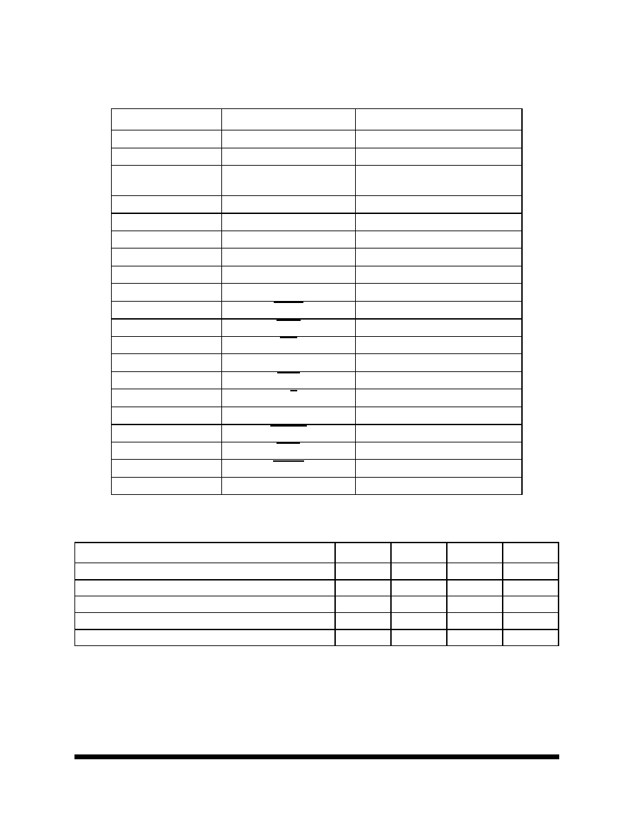
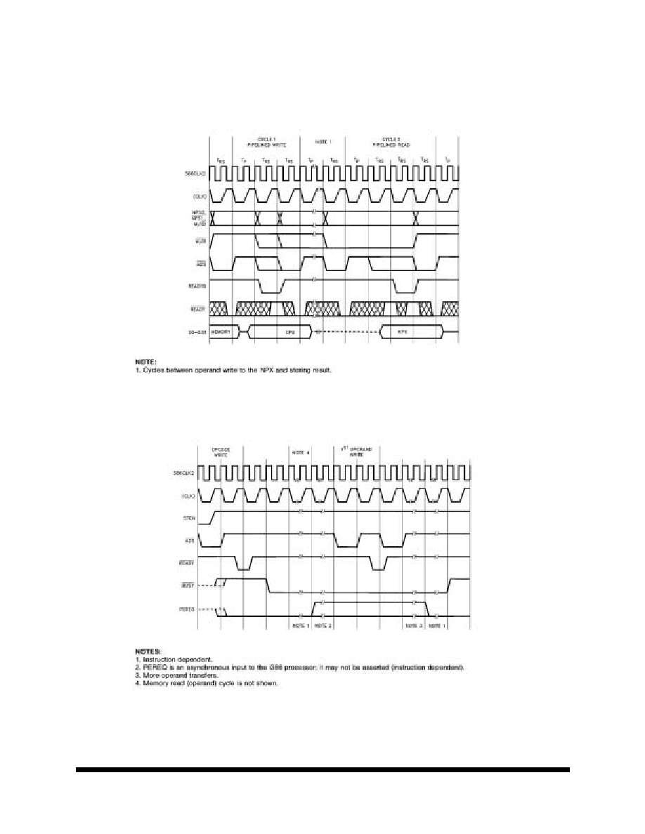
T
ABLE
1. P
INOUT
D
ESCRIPTION
P
IN
S
YMBOL
D
ESCRIPTION
1, 12, 19, 21, 35, 49, 53, 56
V
SS
Ground
2, 13, 20, 32, 36, 39, 52, 68
V
CC
Positive Power Supply
3-11, 18, 22-31, 33, 34, 37,
38, 40, 41, 64-67
D4-D12, D15, D16-25, D26, D27,
D28, D29, D30, D31, D0-D3
Data Bus
42
CKM
Clock Mode
43
386CLK2
386 CPU Clock 2
44
387CLK2
387 MCP Clock 2
45
RESETIN
System Reset
46
NC
Not Connected
47 59
Tie High
Tie High
48
READY
Bus Ready Input
50
CMD0
Command
51
ADS
Address Strobe
54
NPS2
MCP Select #2
55
NPS1
MCP Select #1
57
W/R
Write/Read
58
STEN
Status Enable
60
READYO
Ready Output
61
BUSY
Busy Status
62
ERROR
Error Status
63
PEREQ
Processor Extension Request
T
ABLE
2. A
BSOLUTE
M
AXIMUM
R
ATINGS
P
ARAMETER
S
YMBOL
M
IN
M
AX
U
NIT
Voltage, any pin, with respect to Ground
V
CC
-0.5
V
CC
+0.5
V
Power Dissipation
P
D
--
1.5
W
Storage Temperature Range
T
S
-65
150
∞
C
Operating Temperature Range
T
A
-55
125
∞
C
Lead Temperature (soldering 10 seconds)
--
260
∞
C
M
e
m
o
r
y
3
05.07.02 REV 1
All data sheets are subject to change without notice
©2002 Maxwell Technologies
All rights reserved.
Math Coprocessor
80387DX
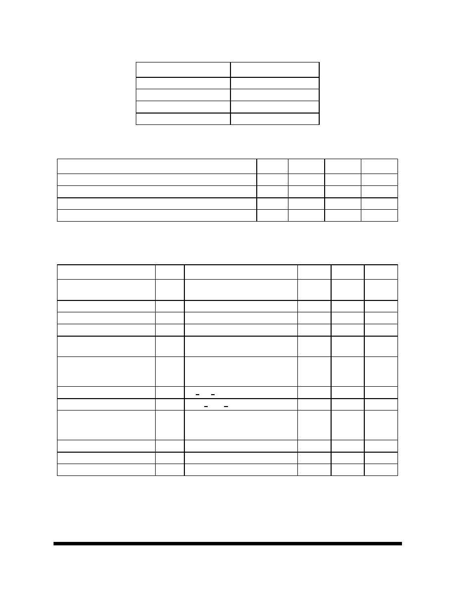
T
ABLE
3. D
ELTA
L
IMITS
P
ARAMETER
V
ARIATION
I
LI
± 1.5 µ A
I
LO
±1.5 µ A
I
CC
CLK2 = 32 MHz
±25 mA
I
CC
CLK2 = 50 MHz
±39 mA
T
ABLE
4. R
ECOMMENDED
O
PERATING
C
ONDITIONS
P
ARAMETER
S
YMBOL
M
IN
M
AX
U
NIT
Supply Voltage
V
CC
4.75
5.25
V
Input Low Voltage
V
IL
-0.3
0.8
V
Input High Voltage
V
IH
2.0
V
CC
+0.3
V
Operating Temperature
T
A
-55
125
∞C
T
ABLE
5. 80387DX DC E
LECTRICAL
C
HARACTERISTICS
(V
CC
= 4.75V
TO
5.25V; T
A
= -55
TO
+125∞C,
UNLESS
OTHERWISE
SPECIFIED
)
P
ARAMETER
S
YMBOL
T
EST
C
ONDITIONS
M
IN
M
AX
U
NIT
Input Low Voltage
V
IL
1
1. This parameter is for all inputs, including 387CLK2 but excluding 386CLK2.
--
--
0.8
--
V
Input High Voltage
V
IH
1
2.0
--
V
386 CLK2 Input Low Voltage
V
CL
--
0.8
V
386 CLK2 Input High Voltage
V
CH
3.7
--
V
Output Low Voltage
V
OL
I
OL
= 4 mA, D0-D31, I
OL
= 2.5 mA
READYO , ERROR, BUSY, PEREQ
--
0.45
V
Output High Voltage
V
OH
I
OH
= -1 mA, D0-D31, I
OH
= -0.6 mA
READYO, READYO, ERROR, BUSY,
PEREQ
2.4
--
V
Input Leakage Current
I
LI
0V < V
IN
< V
CC
±15
µ A
Output Leakage Current
I
LO
0.45V < V
OUT
< V
CC
--
±15
µ A
Power Supply Current
I
CC
CLK2 = 32 MHz
CLK2 = 40 MHz
CLK2 = 50 MHz
2
2. Icc is measured at steady state, maximum capacitive loading on the outputs, and worst-case DC level at the inputs;
386CLK2 at the same frequency as 387CLK2.
--
--
--
250
310
390
mA
Input Capacitance
3
3. Guaranteed By Design
C
IN
F
C
= 1 MHz
--
10
pF
Output Capacitance
3
C
O
F
C
= 1 MHz
--
12
pF
CLK2 Capacitance
3
C
CLK
F
C
= 1 MHz
--
20
pF
M
e
m
o
r
y
4
05.07.02 REV 1
All data sheets are subject to change without notice
©2002 Maxwell Technologies
All rights reserved.
Math Coprocessor
80387DX
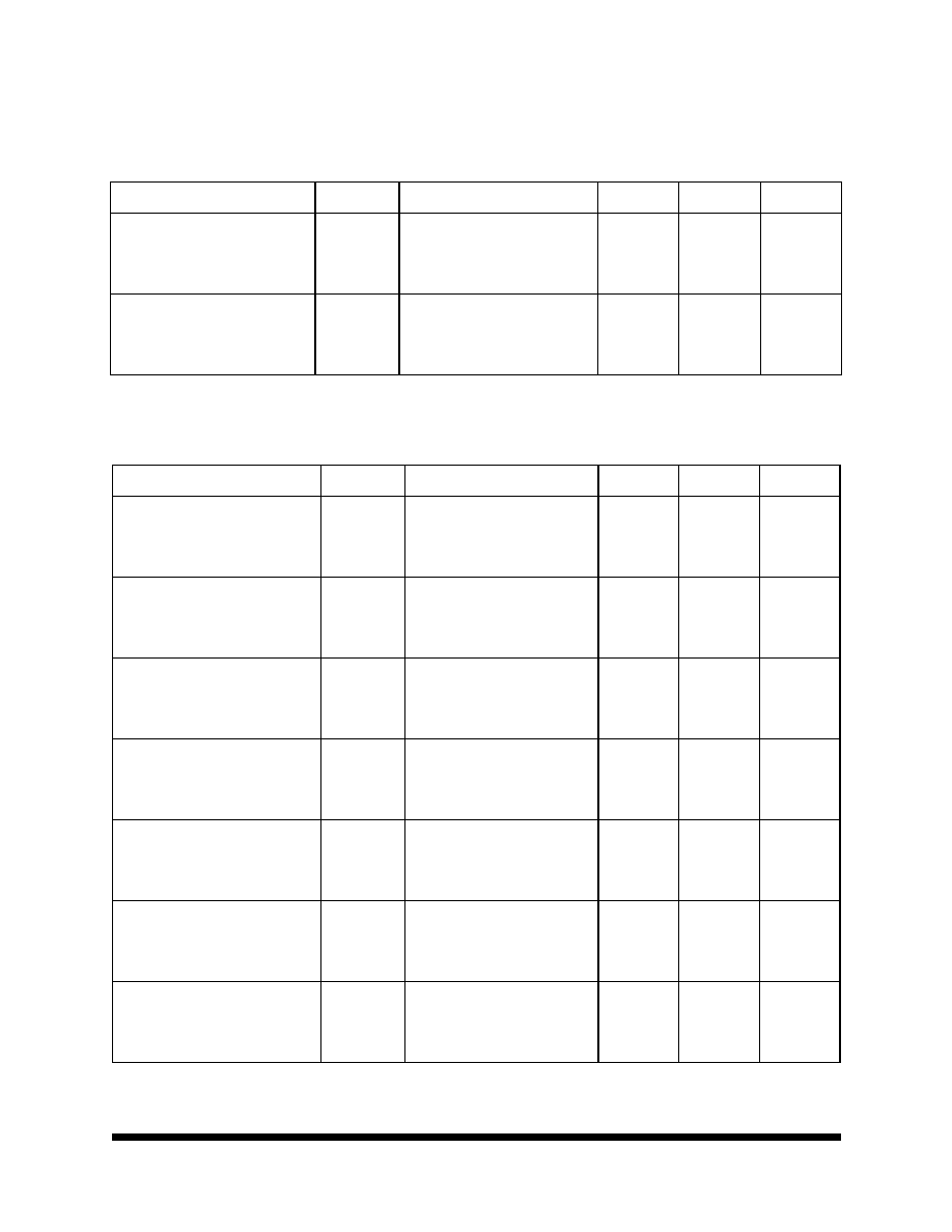
T
ABLE
6. 80387DX C
OMBINATIONS
OF
B
US
I
NTERFACE
AND
E
XECUTION
S
PEEDS
(V
CC
= 4.75V
TO
5.25V; T
A
= -55
TO
+125∞C,
UNLESS
OTHERWISE
SPECIFIED
)
P
ARAMETER
S
YMBOL
T
EST
C
ONDITIONS
M
IN
M
AX
U
NIT
Bus INterface Unit
-16
-20
-25
16
20
25
--
--
--
MHz
Execution Unit
-16
-20
-25
16
20
25
--
--
--
MHz
T
ABLE
7. 80387DX T
IMING
R
EQUIREMENTS
OF
T
HE
E
XECUTION
U
NIT
(V
CC
= 4.75V
TO
5.25V; T
A
= -55
TO
+125∞C,
UNLESS
OTHERWISE
SPECIFIED
)
P
ARAMETER
S
YMBOL
T
EST
C
ONDITION
M
IN
M
AX
U
NIT
387CLK2 Period
1
-16
-20
-25
1. Guaranteed By Design
t
1
At 2V
31
25
20
125
125
125
ns
387CLK2 High Time
-16
-20
-25
t
2a
At 2V
9
8
7
--
--
--
ns
387CLK2 High Time
1
-16
-20
-25
t
2b
At 3.7V
5
5
4
--
--
--
ns
387CLK2 Low Time
-16
-20
-25
t
3a
At 2V
9
8
7
--
--
--
ns
387CLK2 Low Time
1
-16
-20
-25
t
3b
At 0.8V
7
6
5
--
--
--
ns
387CLK2 Fall Time
1
-16
-20
-25
t
4
At 3.7V to 0.8V
--
--
--
8
8
7
ns
387CLK2 Rise Time
1
-16
-20
-25
t
5
At 0.8V to 3.7V
--
--
--
8
8
7
ns

M
e
m
o
r
y
5
05.07.02 REV 1
All data sheets are subject to change without notice
©2002 Maxwell Technologies
All rights reserved.
Math Coprocessor
80387DX
T
ABLE
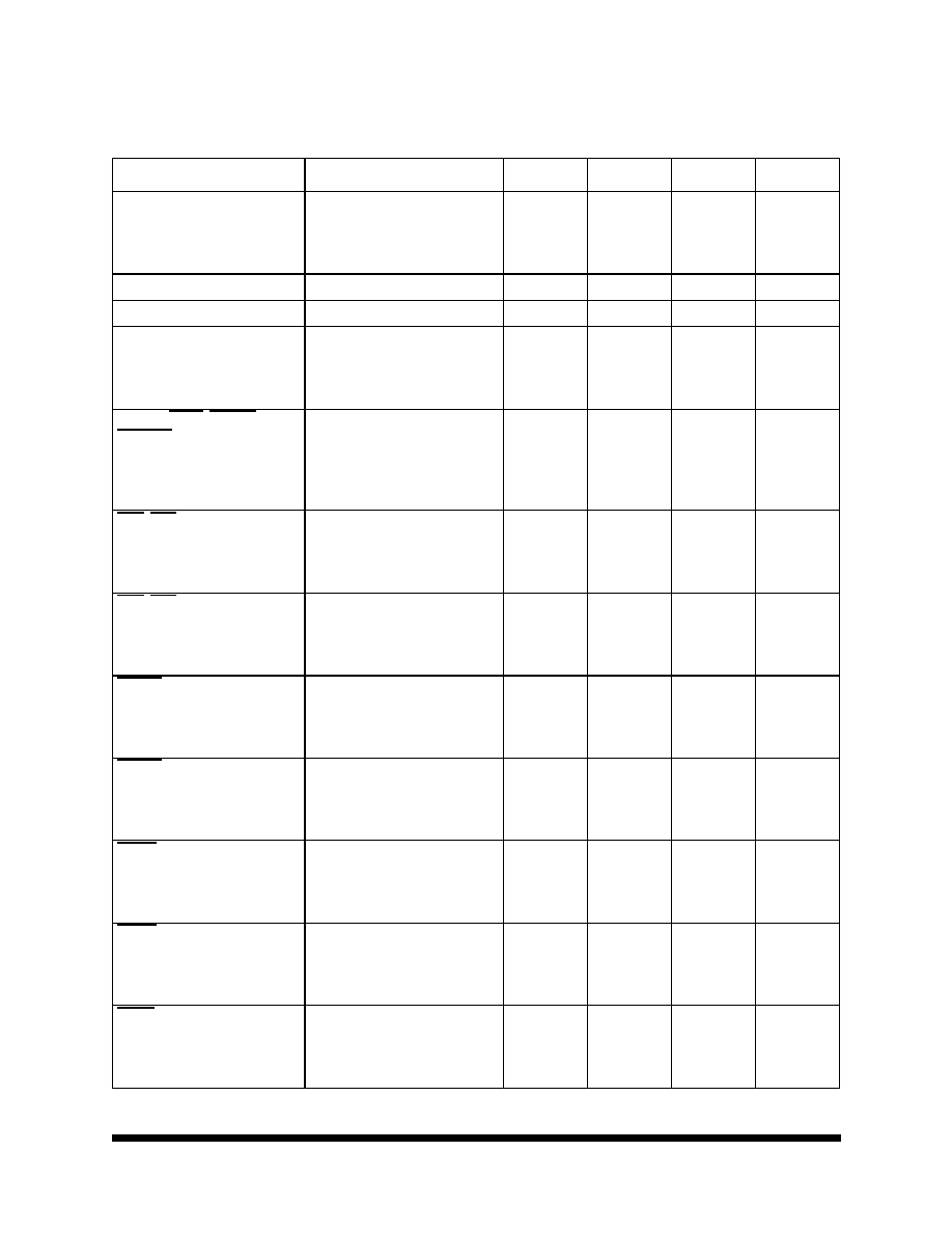
8. 80387DX T
IMING
R
EQUIREMENTS
OF
T
HE
B
US
I
NTERFACE
U
NIT
(O
UTPUT
T
RIP
L
EVEL
= 1.5V)
(V
CC
= 4.75V
TO
5.25V; T
A
= -55
TO
+125∞C,
UNLESS
OTHERWISE
SPECIFIED
)
P
ARAMETER
C
ONDITIONS
S
YMBOL
M
IN
M
AX
U
NIT
386CLK2 Period
1
-16
-20
-25
At 2.0V
t
1
31
25
20
125
125
125
ns
386CLK2 High Time
-16
-20
-25
At 2.0V
t
2a
9
8
7
--
--
--
ns
386CLK2 High Time1
-16
-20
-25
At 3.7V
t
2b
5
5
4
--
--
--
ns
386CLK2 Low Time
-16
-20
-25
At 2V
t
3a
9
8
7
--
--
--
ns
386CLK2 Low Time
1
-16
-20
-25
At 0.8V
t
3b
7
6
5
--
--
--
ns
386CLK2 Fall Time
1
-16
-20
-25
At 3.7V to 0.8V
t
4
--
--
--
8
8
7
ns
386CLK2 Rise Time
1
-16
-20
-25
At 0.8V to 3.7V
t
5
--
--
--
8
8
7
ns
386 CLK2/387CLK2 Ratio
--
10/16
14/10
--
READYO Out Delay
-16
-20
-25
C
L
= 50 pF
t
7
4
3
3
34
31
24
ns
PEREQ, ERROR Out Delay
-16
-20
-25
C
L
= 50 pF
t
7
5
5
4
34
34
33
ns
BUSY Out Delay
-16
-20
-25
C
L
= 50 pF
t
7
5
5
4
34
29
29
ns
M
e
m
o
r
y
6
05.07.02 REV 1
All data sheets are subject to change without notice
©2002 Maxwell Technologies
All rights reserved.
Math Coprocessor
80387DX
D31 - D0 Out Delay
-16
-20
-25
C
L
= 50 pF
t
8
1
1
0
54
54
50
ns
D31 - D0 Setup Time
t
10
11
ns
D31 - D0 Hold Delay
t
11
11
ns
D31 - D0 Float Time
-16
-20
-25
C
L
= 50 pF
2
t
12
6
6
5
33
27
24
ns
PEREQ, BUSY, ERROR,
READYO Float Time
1
-16
-20
-25
C
L
= 50 pF
1
t
13
1
1
1
60
50
40
ns
ADS, W/R Setup Time
-16
-20
-25
t
14
26
21
16
--
--
--
ns
ADS, W/R Hold Time
-16
-20
-25
t
15
5
5
4
--
--
--
ns
READY SetupTime
-16
-20
-25
t
16
21
12
9
--
--
--
ns
READY Hold Time
-16
-20
-25
t
17
4
4
4
--
--
--
ns
CMDO SetupTime
-16
-20
-25
t
16
21
19
16
--
--
--
ns
CMDO HoldTime
-16
-20
-25
t
17
2
4
4
--
--
--
ns
NPS1, NPS2 Setup Time
-16
-20
-25
t
16
21
19
16
--
--
--
ns
T
ABLE
8. 80387DX T
IMING
R
EQUIREMENTS
OF
T
HE
B
US
I
NTERFACE
U
NIT
(O
UTPUT
T
RIP
L
EVEL
= 1.5V)
(V
CC
= 4.75V
TO
5.25V; T
A
= -55
TO
+125∞C,
UNLESS
OTHERWISE
SPECIFIED
)
P
ARAMETER
C
ONDITIONS
S
YMBOL
M
IN
M
AX
U
NIT
M
e
m
o
r
y
7
05.07.02 REV 1
All data sheets are subject to change without notice
©2002 Maxwell Technologies
All rights reserved.
Math Coprocessor
80387DX
NPS1, NPS2 Hold Time
-16
-20
-25
t
17
2
2
4
--
--
--
ns
STEN Setup Time
-16
-20
-25
t
16
21
21
15
--
--
--
ns
STEN Hold Time
-16
-20
-25
t
17
2
2
4
--
--
--
ns
RESETIN Setup Time
-16
-20
-25
t
18
13
12
10
--
--
--
ns
RESETIN Hold Time
-16
-20
-25
t
19
4
4
3
--
--
--
ns
1. Guaranteed By Design
2. Float condition occurs when maximum output current becomes less than I
LO
in magnitude. Float Delay is not tested.
T
ABLE
9. 80387DX T
IMING
R
EQUIREMENT
OF
O
THER
P
ARAMETER
P
ARAMETER
S
YMBOL
M
IN
M
AX
U
NIT
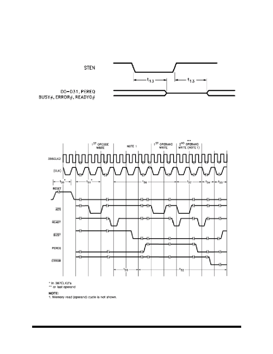
RESETIN Duration
t
30
40
(387 CLK2)
RESETIN Inactive to First Opcode Write
t
31
50
(387 CLK2)
BUSY Duration
t
32
6
(386 CLK2)
ERROR Inactive to BUSY Inactive
t
33
6
(386 CLK2)
PEREQ Inactive to ERROR Active
t
34
6
(386 CLK2)
READY Active to Busy Active
t
35
4
4
(386 CLK2)
READY Minimum Time from Opcode Write to Opcode to Opcode/
Operand Write
t
36
6
(386 CLK2)
READY Minimum Time from Operand Write to Operand Write
t
37
8
(386 CLK2)
T
ABLE
8. 80387DX T
IMING
R
EQUIREMENTS
OF
T
HE
B
US
I
NTERFACE
U
NIT
(O
UTPUT
T
RIP
L
EVEL
= 1.5V)
(V
CC
= 4.75V
TO
5.25V; T
A
= -55
TO
+125∞C,
UNLESS
OTHERWISE
SPECIFIED
)
P
ARAMETER
C
ONDITIONS
S
YMBOL
M
IN
M
AX
U
NIT
M
e
m
o
r
y
8
05.07.02 REV 1
All data sheets are subject to change without notice
©2002 Maxwell Technologies
All rights reserved.
Math Coprocessor
80387DX
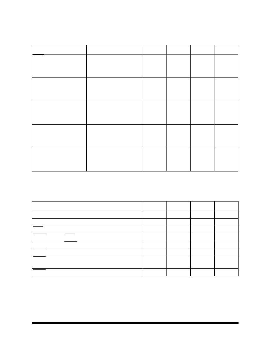
F
IGURE
1. T
IMING
D
IAGRAMS
- F
AST
T
RANSITIONS
TO
AND
FROM
P
IPELINED
C
YCLES
M
e
m
o
r
y
9
05.07.02 REV 1
All data sheets are subject to change without notice
©2002 Maxwell Technologies
All rights reserved.
Math Coprocessor
80387DX
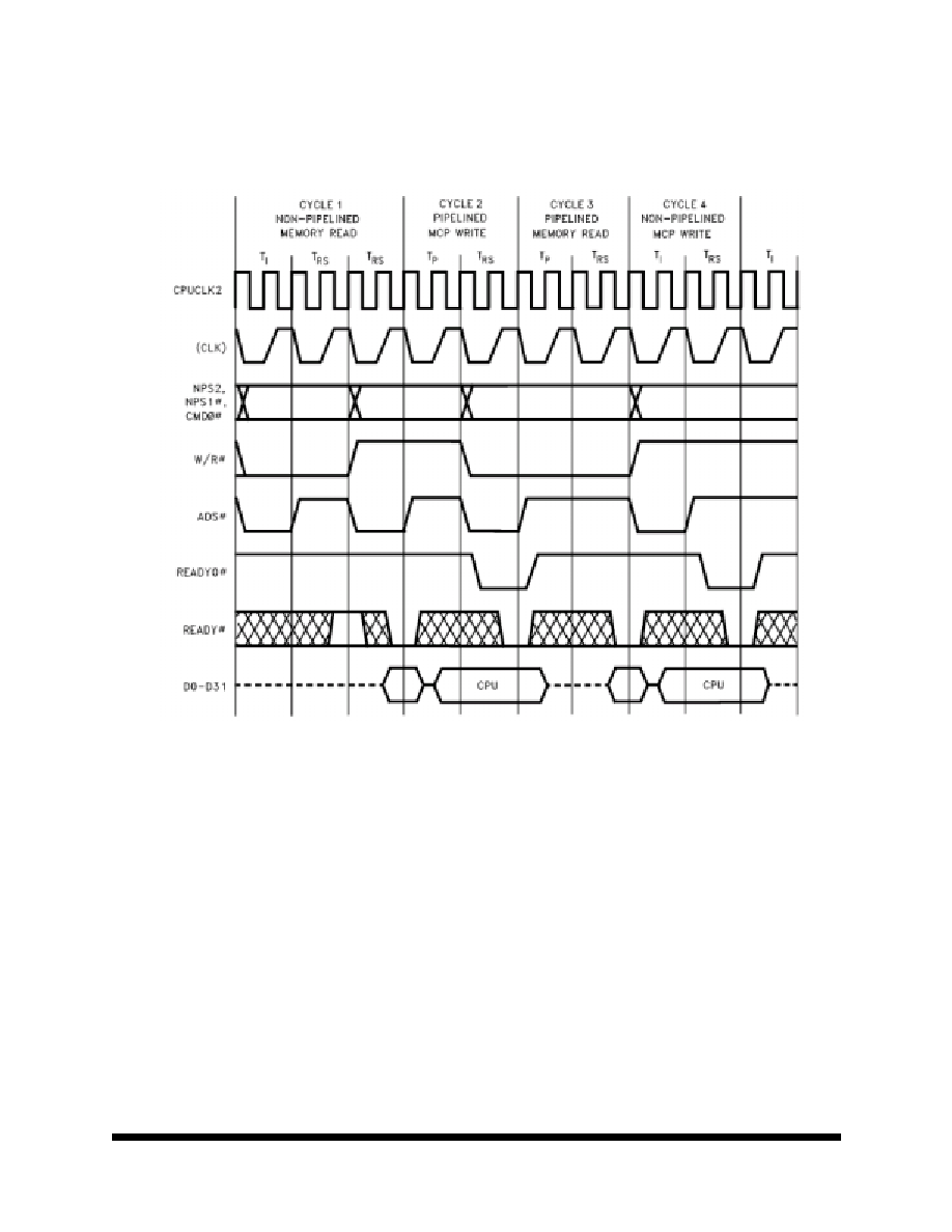
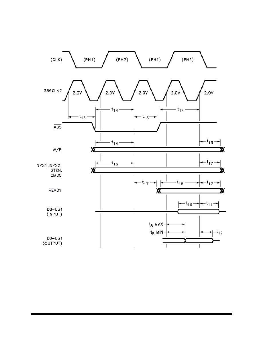
F
IGURE
2. T
IMING
D
IAGRAM
≠ N
ON
-
PIPELINED
R
EAD
AND
W
RITE
C
YCLES
M
e
m
o
r
y
10
05.07.02 REV 1
All data sheets are subject to change without notice
©2002 Maxwell Technologies
All rights reserved.
Math Coprocessor
80387DX
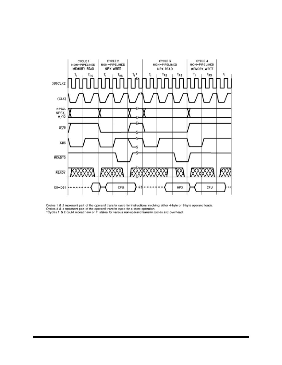
F
IGURE
3. T
IMING
D
IAGRAM
≠ P
IPLINED
C
YCLES
WITH
W
AIT
S
TATES
F
IGURE
4. T
IMING
D
IAGRAM
≠ STEN, BUSY,
AND
PEREQ T
IMING
R
ELATIONSHIP

M
e
m
o
r
y
11
05.07.02 REV 1
All data sheets are subject to change without notice
©2002 Maxwell Technologies
All rights reserved.
Math Coprocessor
80387DX
F
IGURE
5. T
IMING
D
IAGRAM
≠ 386CLK2/387CLK2 W
AVEFORM
AND
M
EASUREMENT
P
OINTS
FOR
I
NPUT
/
O
UTPUT
AC S
PECIFICATIONS
F
IGURE
6. T
IMING
D
IAGRAM
≠ T
EST
C
IRCUIT
M
e
m
o
r
y
12
05.07.02 REV 1
All data sheets are subject to change without notice
©2002 Maxwell Technologies
All rights reserved.
Math Coprocessor
80387DX
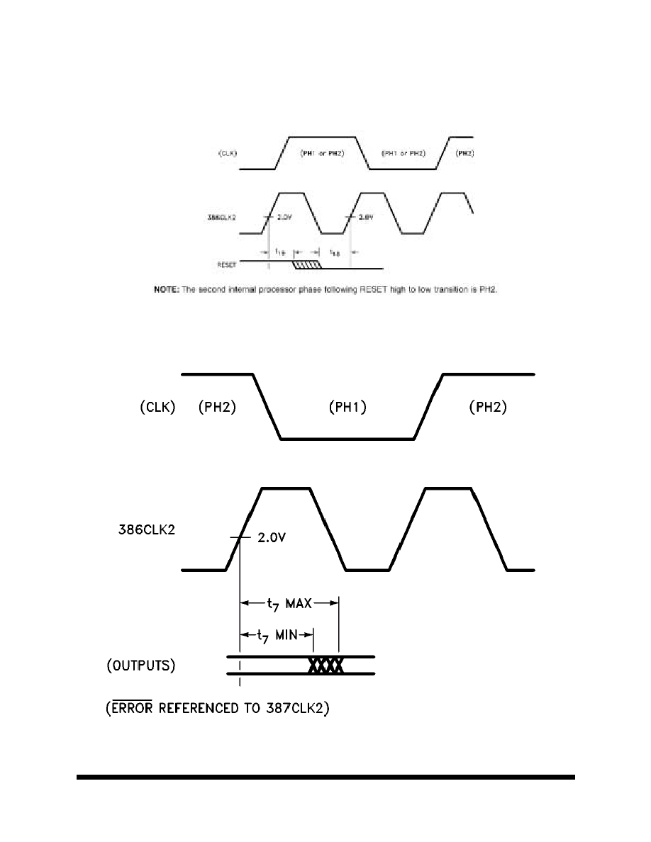
F
IGURE
7. T
IMING
D
IAGRAM
≠ R
ESET
F
IGURE
8. T
IMING
D
IAGRAM
≠ O
UTPUT
M
e
m
o
r
y
13
05.07.02 REV 1
All data sheets are subject to change without notice
©2002 Maxwell Technologies
All rights reserved.
Math Coprocessor
80387DX
F
IGURE
9. T
IMING
D
IAGRAM
≠ I
NPUT
AND
I/O S
IGNALS
M
e
m
o
r
y
14
05.07.02 REV 1
All data sheets are subject to change without notice
©2002 Maxwell Technologies
All rights reserved.
Math Coprocessor
80387DX
F
IGURE
10. T
IMING
D
IAGRAM
≠ F
LOAT
FROM
STEN
F
IGURE
11. T
IMING
D
IAGRAM
≠ O
THER
P
ARAMETERS

M
e
m
o
r
y
15
05.07.02 REV 1
All data sheets are subject to change without notice
©2002 Maxwell Technologies
All rights reserved.
Math Coprocessor
80387DX
Note: All dimensions in inches.
Q68-01
14 P
IN
R
AD
-P
AK
Æ F
LAT
P
ACKAGE
S
YMBOL
D
IMENSION
M
IN
N
OM
M
AX
A
0.121
0.135
0.145
b
0.016
0.018
0.020
c
0.008
0.010
0.012
D
0.940
0.950
0.960
D1
0.800 BSC
e
0.050 BSC
S1
0.013
0.066
--
F1
0.645
0.650
0.655
F2
0.645
0.650
0.655
L
0.477
0.487
0.497
A1
0.080
0.090
0.100
N
68

M
e
m
o
r
y
16
05.07.02 REV 1
All data sheets are subject to change without notice
©2002 Maxwell Technologies
All rights reserved.
Math Coprocessor
80387DX
Important Notice:
These data sheets are created using the chip manufacturer's published specifications. Maxwell Technologies verifies
functionality by testing key parameters either by 100% testing, sample testing or characterization.
The specifications presented within these data sheets represent the latest and most accurate information available to
date. However, these specifications are subject to change without notice and Maxwell Technologies assumes no
responsibility for the use of this information.
Maxwell Technologies' products are not authorized for use as critical components in life support devices or systems
without express written approval from Maxwell Technologies.
Any claim against Maxwell Technologies must be made within 90 days from the date of shipment from Maxwell Tech-
nologies. Maxwell Technologies' liability shall be limited to replacement of defective parts.
M
e
m
o
r
y
17
05.07.02 REV 1
All data sheets are subject to change without notice
©2002 Maxwell Technologies
All rights reserved.
Math Coprocessor
80387DX
Product Ordering Options
Model Number
Feature
Option Details
80387DX RP
Q
X
Screening Flow
Package
Radiation Feature
Base Product
Nomenclature
Monolithic
S = Maxwell Class S
B = Maxwell Class B
E = Engineering (testing @ +25∞C)
I = Industrial (testing @ -55∞C,
+25∞C, +125∞C)
Q = Quad Flat Pack
RP = R
AD
-P
AK
Æ package
Math Coprocessor