 | –≠–ª–µ–∫—Ç—Ä–æ–Ω–Ω—ã–π –∫–æ–º–ø–æ–Ω–µ–Ω—Ç: 81840RPQK | –°–∫–∞—á–∞—Ç—å:  PDF PDF  ZIP ZIP |

1
M
e
m
o
r
y
All data sheets are subject to change without notice
(858) 503-3300 - Fax: (858) 503-3301 - www.maxwell.com
128 Channel Multiplexer
81840
©2021 Maxwell Technologies
All rights reserved.
06.17.02 REV 5
F
EATURES
:
∑
128 channel multiplexer, MCM
∑
Package:
- 256 pin R
AD
-P
AK
Æ quad flat pack
∑
Total dose hardness:
- > 300 krads(Si)
∑
- Dependent upon orbit
∑
Excellent Single Event Effects:
SEL: > 110 MeV-cm
2
/mg
SEU: > 110 MeV-cm
2
/mg
D
ESCRIPTION
:
Maxwell Technologies' 81840 high-performance 128-channel
multiplexer features a typical 300 krad (Si) total dose tolerance.
This datasheet defines the design, performance, and test require-
ments for a hermetic, telemetry multiplexer, multi-chip-module
(MCM), utilizing chip and wire technology to be used in space
systems. The 81840 is intended for use in the environments
encountered by high reliability spacecraft applications. The pat-
ented radiation-hardened R
AD
-P
AK
Æ technology incorporates radi-
ation shielding in the microcircuit package. Capable of surviving
in-space environment, the 81840 is ideal for satellite, spacecraft,
and space probe missions. It is available up to Class K screening.
16:1
1840A
16:1
1840A
16:1
1840A
16:1
1840A
16:1
1840A
16:1
1840A
16:1
1840A
(8 TOTAL 1840A's)
GRND
5
4
GRND
5
4
GRND
GRND
OUT
IN
IN
OUT
8
8
5
16
16
GRND
8
5
GRND
8
5
IN
OUT
8
8
GRND
8
5
IN
NEGATIVE
OUTPUT
POSITIVE
OUTPUT
OUT
4
4
8
4
ADDRESS ENABLE
128 TOTAL
ANALOG INPUTS
GROUND
REFERENCE
INPUTS
SPARE
INPUTS
ADDRESS
ENABLE
SPARE
OUTPUT
ADDRESS
ENABLE
7
SPARE
INPUT
VREF
(+5V)
GRND
ADDRESS
ENABLE
SPARE
OUTPUT
ADDRESS
ENABLE
8
8
IN
IN
ADDRESS ENABLE
COMMON TO ALL
INPUT MUX's
CLAMP/
PRECHARGE
ADDRESS
ENABLE
CASCADE
INPUT
BYPASS
V+
(+15V)
V-
(-15V)
+
-
IN
IN
See page 2 for pin assignments.
81840

M
e
m
o
r
y
2
All data sheets are subject to change without notice
©2021 Maxwell Technologies
All rights reserved.
128 Channel Multiplexer
81840
06.17.02 REV 5
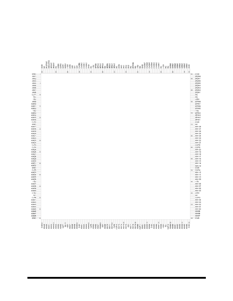
81840 Pinout Diagram

M
e
m
o
r
y
3
All data sheets are subject to change without notice
©2021 Maxwell Technologies
All rights reserved.
128 Channel Multiplexer
81840
06.17.02 REV 5
T
ABLE
1. P
INOUT
D
ESCRIPTION
P
IN
S
YMBOL
D
ESCRIPTION
1, 23, 42, 64, 65, 81, 112, 128, 129, 151, 171,
192, 193, 213, 236, 256
GND
2-9, 13-16, 18-21, 24-31, 34-41, 44-47, 49-52,
56-63, 66-73, 77-80, 82-85, 87-90, 92-95, 98-
101, 103-106, 108-111, 113-116, 120-127, 130-
137, 141-144, 146-149, 152-159, 162-169,
AIN1 - 128
10, 22, 32, 33, 43, 55
CLP1 - 6
11, 54, 75, 96, 97, 107, 117, 118, 138, 139, 150,
160, 161, 170, 182, 203, 214, 223, 228, 233,
240, 244, 249
NC
12, 53, 76, 117, 140, 181, 204, 245
+15V
17, 48, 91, 102, 145, 176, 215, 234
-15V
172-175, 177-180
SP1IN1 - 8
184-191
SP2IN1 - 8
194-201
GRIN1 - 8
183, 202, 250
+5V
206-212
CASIN1 - 7
216
H1EN
217
BYPASS
218
SP2EN
224
SP1EN
222-219
HA0 - 3
227-225
SP2A0 - 2
229
CASEN
233-230
SP1A0 - 2
235
L1EN
239-237
CASA0 - 2
243-241
LA0 - 2
248-246
GRA0 - 2
252
SP1OUT
251
SP2OUT
253
NEGATIVE
254
POSITIVE
255
GREN

M
e
m
o
r
y
4
All data sheets are subject to change without notice
©2021 Maxwell Technologies
All rights reserved.
128 Channel Multiplexer
81840
06.17.02 REV 5
T
ABLE
2. 81840 A
BSOLUTE
M
AXIMUM
R
ATINGS1
,
2
,
3
,
4
1. The LMUX MCM is designed to operate with power supply voltages ranging
from ±5.2V to ±20VDC.
2. The maximum voltage each input AIN(128:1) may see without damage is
+35V to -35V with respect to ground.
3. Stresses above the absolute maximum rating may cause permanent damage
to the device. Extended operation at the maximum levels may degrade per-
formance and affect reliability.
4. T
A
= 25∞C unless otherwise specified.
E
NVIRONMENT
R
ANGES
V+ To Ground
20V
V- To Ground
-20V
Input Overvoltage, AIN(1) to AIN(128)
35V to-35V
(Power ON or OFF)
Input Overvoltage, Logic Inputs
4V over V
REF
and -4V below
Grd
Power Dissipation
500mW Maximum
Storage Temperature
-65 to 150∞C
Operating Temperature
-55 to 125∞C
T
ABLE
3. 81840 AC E
LECTRICAL
C
HARACTERISTICS
P
ARAMETER
T
EST
C
ONDITIONS
S
UBGROUPS
T
EST
L
IMITS
U
NITS
T
A
= 25∞C
T
A
= 125∞C
T
A
= -55
∞
C
M
IN
M
AX
M
IN
M
AX
M
IN
M
AX
Address Input to I/O Channels
Prop. Delay
t
ON(A)
t
OFF(A)
V
IN
= 5.0V
R
L
= 5k
>
C
L
= 50pF
9, 10, 11
--
--
1500
1500
--
--
1500
1500
--
--
1500
1500
nsec
Enable to I/O
t
ON(EN)
t
OFF(EN)
V
IN
= 5.0V
R
L
= 5k
>
C
L
= 50 pF
9, 10, 11
--
--
1500
1500
--
--
1500
1500
--
--
1500
1500
nsec
On Channel Isolation
V
ISO(ON)
All enable = 0.8V
V
IN
= 3V
RMS
@
500kHz
1
1. Controlled by design, not directly tested.
4, 5, 6
45
--
45
--
45
--
db
Off Channel Isolation
V
ISO(OFF)
All enable = 4.0V
V
IN
= 3V
RMS
@
500kHz
1
4, 5, 6
45
--
45
--
45
--
db

M
e
m
o
r
y
5
All data sheets are subject to change without notice
©2021 Maxwell Technologies
All rights reserved.
128 Channel Multiplexer
81840
06.17.02 REV 5
T
ABLE
4. D
ELTA
L
IMITS
P
ARAMETER
V
ARIATION
I
S+
±10%
I
S-
±10%
I
SB+
±10%
I
SB-
±10%
T
ABLE
5. 81840 E
LECTRICAL
T
EST
T
ABLE
P
ARAMETER
T
EST
C
ONDITIONS
S
UBGROUPS
T
EST
L
IMITS
U
NITS
T
A
= 25∞C
T
A
= 125∞C
T
A
=-55∞C
M
IN
M
AX
M
IN
M
AX
M
IN
M
AX
Analog Signal Range, V
0
-15
15
-15
15
-15
15
V
Bypass Output, On-Resis-
tance, 5V, R
BP(ON)
V
IN
= 5V
I
OUT
= -1.0mA
1, 2, 3
2.0
6.0
2.0
6.0
2.0
6.0
k
Positive Output, On-Resis-
tance, 5V, R
PO(ON)
V
IN
= 5V
I
OUT
= -1.0mA
1, 2, 3
3.0
9.0
3.0
9.0
3.0
9.0
k
Negative or Spare Output, On-
Resistance,
5V, R
NS(ON)
V
IN
= 5V
I
OUT
= -1.0mA
1, 2, 3
1.0
3.0
1.0
3.0
1.0
3.0
k
Bypass Output, On-Resis-
tance, -5V, R
BP(ON)
V
IN
= -5V
I
OUT
= 1.0mA
1, 2, 3
2.0
6.0
2.0
6.0
2.0
6.0
k
Positive Output, On-Resis-
tance, -5V, R
PO(ON)
V
IN
= -5V
I
OUT
= 1.0mA
1, 2, 3
3.0
9.0
3.0
9.0
3.0
9.0
k
Negative or Spare Output, On-
Resistance,
-5V, R
NS(ON)
V
IN
= -5V
I
OUT
= 1.0mA
1, 2, 3
1.0
3.0
1.0
4.0
1.0
4.0
k
Input Leakage Current, LA0,
LA1, LA2, HA0, LIEN, Address
or Enable Pins, I
AH
, I
AL
All unused pins = Ground
1, 2, 3
-100
100
-200
200
-200
200
nA
Input Leakage Current, All
Other Address or Enable Pins
I
AH,
I
AL
All unused pins =
Ground
1, 2, 3
-100
100
-200
200
-200
200
nA
Leakage Current into MUX
Input Channels, AINxx, GRINx,
SP1INx, SP2INx, CASINx,
+I
S(OFF)
V
IN
= 10V,
All enables = 4.0V
All unused inputs &
outouts = -10V
1, 2, 3
-20
20
-100
100
-100
100
nA
Leakage Current into MUX
Input Channels, AINxx, GRINx,
SP1INx, SP2INx, CASINx, -
I
S(OFF)
V
IN
= -10V
All enables = 4.0V
All unused inputs &
outputs = +10V
1, 2, 3
-20
20
-100
100
-100
100
nA


