1
M
e
m
o
r
y
All data sheets are subject to change without notice
(619) 503-3300 - Fax: (619) 503-3301 - www.maxwell.com
16 Megabit (512K x 32-Bit)
89C1632
©2005 Maxwell Technologies.
All rights reserved.
MCM SRAM
01.10.05 Rev 3
F
EATURES
:
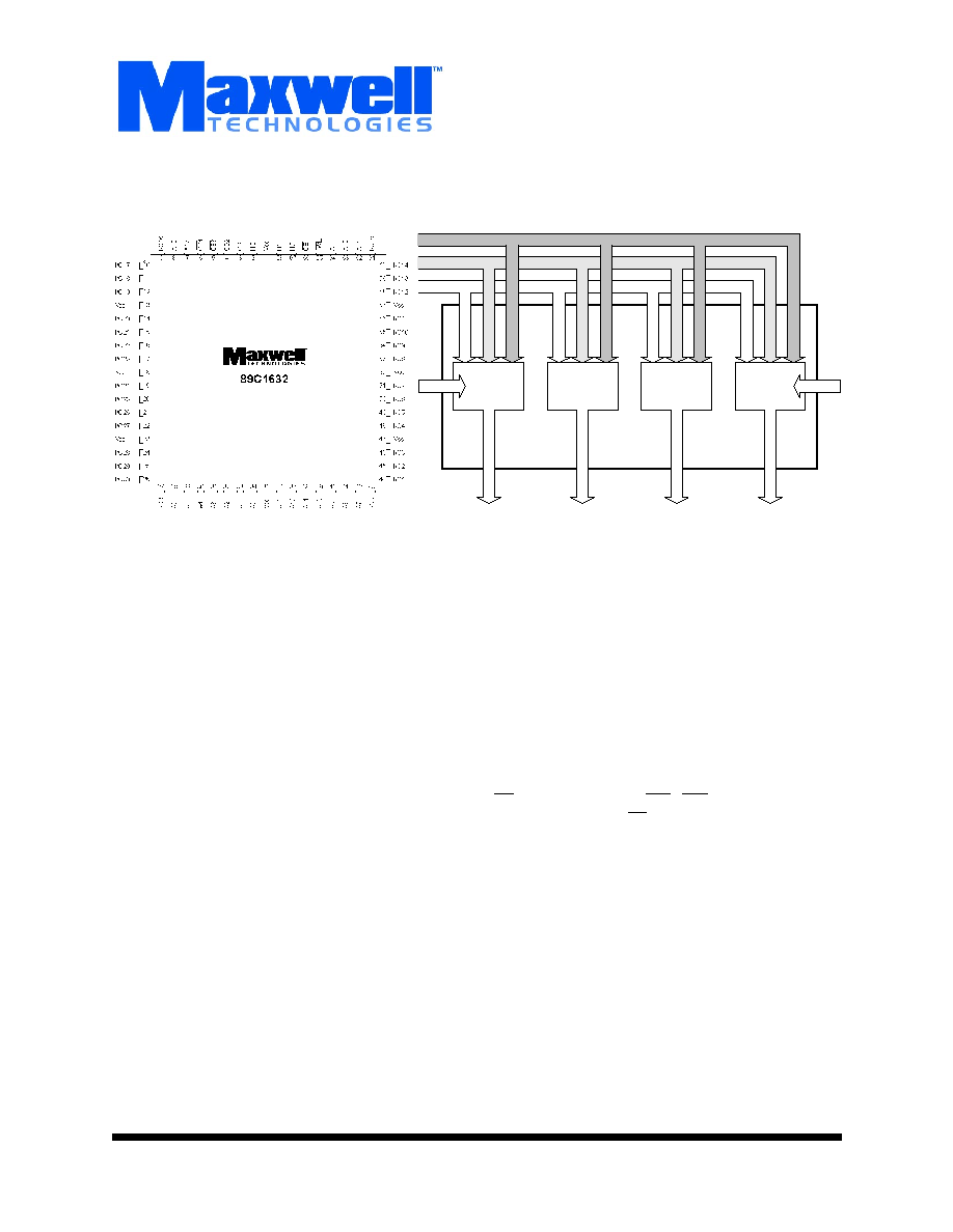
∑ Four 512k x 8 SRAM architecture
∑ R
AD
-P
AK
Æ technology hardens against natural space radia-
tion technology
∑ Total dose hardness:
- > 100 krad (Si), depending upon space mission
∑ Excellent Single Event Effects:
- SEL > 101MeV-cm
2
/mg
- SEU threshold = 3 MeV-cm
2
/mg
- SEU saturated cross section: 6E-9 cm
2
/bit
∑ Package: 68-pin quad flat package
∑ Fast access time: 20, 25 and 30 ns
∑ Completely static memory - no clock or timing strobe
required
∑ Internal bypass capacitor
∑ High-speed silicon-gate CMOS technology
∑ 5V or 3V ± 10% power supply
∑ Equal address and chip enable access times
∑ Three-state outputs
∑ All inputs and outputs are TTL compatible
D
ESCRIPTION
:
Maxwell Technologies' 89C1632 high-performance 16 Mega-
bit Multi-Chip Module (MCM) Static Random Access Memory
features a greater than 100 krad (Si) total dose tolerance,
depending upon space mission. The four 4-Megabit SRAM die
and bypass capacitors are incorporated into a high-reliable
hermetic quad flat-pack ceramic package. With high-perfor-
mance silicon-gate CMOS technology, the 89C1632 reduces
power consumption and eliminates the need for external
clocks or timing strobes. It is equipped with output enable
(OE) and four byte enable (CS1 - CS4) inputs to allow greater
system flexibility. When OE input is high, the output is forced
to high impedance.
Maxwell Technologies' patented R
AD
-P
AK
Æ packaging technol-
ogy incorporates radiation shielding in the microcircuit pack-
age. In a GEO orbit, R
AD
-P
AK
provides true greater than 100
krad (Si) total radiation dose tolerance, dependent upon space
mission. It eliminates the need for box shielding while provid-
ing the required radiation shielding for a lifetime in orbit or a
space mission. This product is available with screening up to
Maxwell Technologies self-defined Class K.
CS 1-4
MCM
OE, WE
Address
4Mb SRAM
4Mb SRAM
4Mb SRAM
4Mb SRAM
Power
Ground
I/O 0-7
I/O 8-15
I/O 16-23
I/O 24-31
16 Megabit (512k x 32-bit) SRAM MCM
Logic Diagram
M
e
m
o
r
y
2
All data sheets are subject to change without notice
©2005 Maxwell Technologies.
All rights reserved.
16 Megabit (512K x 32-Bit) MCM SRAM
89C1632
01.10.05 Rev 3
T
ABLE
1. P
INOUT
D
ESCRIPTION
P
IN
S
YMBOL
D
ESCRIPTION
34-28, 42-36, 62-64, 7, 8
A0-A18
Address Enable
65
WE
WriteEnable
66
OE
Output Enable
3-6
CS1 - CS4
Chip Enable
43-46, 48-56, 58-61, 9-12,
14-17, 19-22, 24-27
I/O0-I/O31
Data Input/Output
2, 67, 68
NC
No Connection
1, 18, 35, 52
V
CC
+5V Power Supply
13, 23, 47, 57
V
SS
Ground
T
ABLE
2. 89C1632 A
BSOLUTE
M
AXIMUM
R
ATINGS
(V
OLTAGE
REFERENCED
TO
V
SS
= 0V)
P
ARAMETER
S
YMBOL
M
IN
M
AX
U
NITS
Power Supply Voltage Relative to V
SS
V
CC
-0.5 +7.0
V
Voltage Relative to V
SS
for Any Pin Except V
CC
V
IN
, V
OUT
-0.5
V
CC
+0.5
V
Power Dissipation
P
D
--
4.0
W
Operating Temperature
T
A
-55
+125
∞
C
Storage Temperature
T
S
-65
+150
∞
C
T
ABLE
3. 89C1632 R
ECOMMENDED
O
PERATING
C
ONDITIONS
(V
CC
= 5.0 + 10%, T
A
= -55
TO
+125
∞
C,
UNLESS
OTHERWISE
NOTED
)
P
ARAMETER
S
YMBOL
M
IN
M
AX
U
NITS
Supply Voltage, (Operating Voltage Range)
V
CC
4.5
5.5
V
Input High Voltage
V
IH
2.2
V
CC
+ 0.5
(1)
1. V
IH
(max) = V
CC
+ 2V ac (pulse width < 10ns) for I < 80 mA.
V
Input Low Voltage
V
IL
-0.5
(2)
2. V
IL
(min) = -2.0V ac; (pulse width < 20 ns) for I < 80 mA.
0.8
V
T
ABLE
4. 89C1632 D
ELTA
L
IMITS
P
ARAMETER
V
ARIATIONL
I
CC
+10% of stated value in table 5

M
e
m
o
r
y
3
All data sheets are subject to change without notice
©2005 Maxwell Technologies.
All rights reserved.
16 Megabit (512K x 32-Bit) MCM SRAM
89C1632
01.10.05 Rev 3
I
SB
+10% of stated value in table 5
I
SB1
+10% of stated value in table 5
I
LI
+10% of stated value in table 5
T
ABLE
5. 89C1632 DC E
LECTRICAL
C
HARACTERISTICS
(V
CC
= 5.0 + 10%, T
A
= -55
TO
+125
∞
C,
UNLESS
OTHERWISE
NOTED
)
P
ARAMETER
S
YMBOL
T
EST
C
ONDITIONS
S
UBGROUPS
M
IN
T
YP
M
AX
U
NITS
Input Leakage Current
I
LI
V
IN
= 0 to V
CC
1, 2, 3
-8.0
--
+8.0
uA
Output Leakage Current
I
LO
CS = V
IH
, V
OUT
= V
SS
to V
CC
1, 2, 3
-8.0
--
+8.0
uA
Average Operating Current
Cycle Time:
20 ns
25 ns
30 ns
I
CC
Min. Cycle, 100% Duty, CS = V
IL
,
I
OUT
= 0 mA
V
IN
= V
IH
or V
IL
1, 2, 3
--
--
--
--
800
760
720
mA
Standby Power Supply Current
I
SB
CS= V
IH
, cycle time > 25ns
1, 2, 3
--
--
240
mA
CMOS Standby Power Supply
Current
I
SB1
CS > V
CC
- 0.2V, f = 0 MHz, V
IN
>
V
CC
- 0.2V or
V
IN
<
0.2V
1, 2, 3
--
--
60
mA
Output Low Voltage
V
OL
I
OL
= + 8.0 mA
1, 2, 3
--
--
0.4
V
Output High Voltage
V
OH
I
OH
= -4.0 mA
1, 2, 3
2.4
--
--
V
Input Capacitance
1
CS1 - CS4,
OE, WE
I/O0-7, I/O8-15, I/O16-23,
I/O24-31
1. Guaranteed by design.
C
IN
V
IN
= 0 V
1, 2, 3
7
28
7
pF
1, 2, 3
Input / Output Capacitance
1
C
OUT
V
I/O
= 0 V
4, 5, 6
8
pF
T
ABLE
6. 89C1632 AC O
PERATING
C
ONDITIONS
AND
C
HARACTERISTICS
(V
CC
= 5.0 + 10%, T
A
= -55
TO
+125
∞
C,
UNLESS
OTHERWISE
NOTED
)
P
ARAMETER
M
IN
T
YP
M
AX
U
NITS
Input Pulse Level
0.0
--
3.0
V
Output Timing Measurement Reference Level
--
--
1.5
V
Input Rise/Fall Time
--
--
3.0
ns
T
ABLE
4. 89C1632 D
ELTA
L
IMITS
P
ARAMETER
V
ARIATIONL
M
e
m
o
r
y
4
All data sheets are subject to change without notice
©2005 Maxwell Technologies.
All rights reserved.
16 Megabit (512K x 32-Bit) MCM SRAM
89C1632
01.10.05 Rev 3
Input Timing Measurement Reference Level
--
--
1.5
V
T
ABLE
7. 89C1632 R
EAD
C
YCLE
(V
CC
= 5.0 + 10%, T
A
= -55
TO
+125
∞
C,
UNLESS
OTHERWISE
NOTED
)
P
ARAMETER
S
YMBOL
S
UBGROUPS
M
IN
T
YP
M
AX
U
NITS
Read Cycle Time
-20
-25
-30
t
RC
9, 10, 11
20
25
30
--
--
--
--
--
--
ns
Address Access Time
-20
-25
-30
t
AA
9, 10, 11
--
--
--
--
--
--
20
25
30
ns
Chip Select to Output
-20
-25
-30
t
CO
9, 10, 11
--
--
--
--
--
--
20
25
30
ns
Output Enable to Output
-20
-25
-30
t
OE
9, 10, 11
--
--
--
--
--
--
10
12
14
ns
Output Enable to Low-Z Output
-20
-25
-30
t
OLZ
9, 10, 11
--
--
--
0
0
0
--
--
--
ns
Chip Enable to Low-Z Output
-20
-25
-30
t
LZ
9, 10, 11
--
--
--
3
3
3
--
--
--
ns
Output Disable to High-Z Output
-20
-25
-30
t
OHZ
9, 10, 11
--
--
--
5
6
8
--
--
--
ns
Chip Disable to High-Z Output
-20
-25
-30
t
HZ
9, 10, 11
--
--
--
5
6
8
--
--
--
ns
Output Hold from Address Change
-20
-25
-30
t
OH
9, 10, 11
3
3
3
--
--
--
--
--
--
ns
T
ABLE
6. 89C1632 AC O
PERATING
C
ONDITIONS
AND
C
HARACTERISTICS
(V
CC
= 5.0 + 10%, T
A
= -55
TO
+125
∞
C,
UNLESS
OTHERWISE
NOTED
)
P
ARAMETER
M
IN
T
YP
M
AX
U
NITS
M
e
m
o
r
y
5
All data sheets are subject to change without notice
©2005 Maxwell Technologies.
All rights reserved.
16 Megabit (512K x 32-Bit) MCM SRAM
89C1632
01.10.05 Rev 3
T
ABLE
8. 89C1632 F
UNCTIONAL
D
ESCRIPTION
CS
WE
OE
M
ODE
I/O P
IN
S
UPPLY
C
URRENT
H
X
1
1. X = don't care.
X
1
Not Select
High-Z
I
SB
, I
SB1
L
H
H
Output Disable
High-Z
I
CC
L
H
L
Read
D
OUT
I
CC
L
L
X
1
Write
D
IN
I
CC
T
ABLE
9. 89C1632 W
RITE
C
YCLE
(V
CC
= 5.0 + 10%, T
A
= -55
TO
+125
∞
C,
UNLESS
OTHERWISE
NOTED
)
P
ARAMETER
S
YMBOL
S
UBGROUPS
M
IN
T
YP
M
AX
U
NITS
Write Cycle Time
-20
-25
-30
t
WC
9, 10, 11
20
25
30
--
--
--
ns
Chip Select to End of Write
-20
-25
-30
t
CW
9, 10, 11
14
17
20
--
--
--
ns
Address Set-up Time
-20
-25
-30
t
AS
9, 10, 11
0
0
0
--
--
--
ns
Address Valid to End of Write
-20
-25
-30
t
AW
9, 10, 11
14
17
20
--
--
--
ns
Write Pulse Width (OE High)
-20
-25
-30
t
WP
9, 10, 11
14
17
20
--
--
--
ns
Write Pulse Width (OE Low)
-20
-25
-30
t
WP1
9, 10, 11
20
25
30
--
--
--
ns
Write Recovery Time
-20
-25
-30
t
WR
9, 10, 11
0
0
0
--
--
--
ns

M
e
m
o
r
y
6
All data sheets are subject to change without notice
©2005 Maxwell Technologies.
All rights reserved.
16 Megabit (512K x 32-Bit) MCM SRAM
89C1632
01.10.05 Rev 3
Write to Output High-Z
-20
-25
-30
t
WHZ
9, 10, 11
--
--
--
5
7
9
--
--
--
ns
Data to Write Time Overlap
-25
-30
t
DW
9, 10, 11
10
12
14
--
--
--
ns
Data Hold from Write Time
-20
-25
-30
t
DH
9, 10, 11
0
0
0
--
--
--
ns
End Write to Output Low-Z
-20
-25
-30
t
OW
9, 10, 11
--
--
--
3
3
3
--
--
--
ns
T
ABLE
9. 89C1632 W
RITE
C
YCLE
(V
CC
= 5.0 + 10%, T
A
= -55
TO
+125
∞
C,
UNLESS
OTHERWISE
NOTED
)
P
ARAMETER
S
YMBOL
S
UBGROUPS
M
IN
T
YP
M
AX
U
NITS

M
e
m
o
r
y
7
All data sheets are subject to change without notice
©2005 Maxwell Technologies.
All rights reserved.
16 Megabit (512K x 32-Bit) MCM SRAM
89C1632
01.10.05 Rev 3
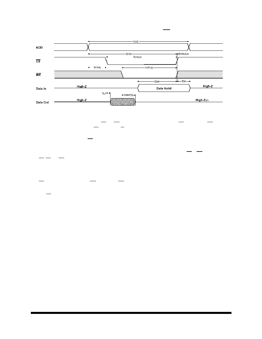
F
IGURE
1. AC T
EST
L
OADS
F
IGURE
2. T
IMING
W
AVEFORM
OF
R
EAD
C
YCLE
(1)
(A
DDRESS
C
ONTROLLED
)
F
IGURE
3. T
IMING
W
AVEFORM
OF
R
EAD
C
YCLE
(2)
(WE = V
IH
)
1. WE is high for read cycle.
2. All read cycle timing is referenced from the last valid address to the first transition address.

M
e
m
o
r
y
8
All data sheets are subject to change without notice
©2005 Maxwell Technologies.
All rights reserved.
16 Megabit (512K x 32-Bit) MCM SRAM
89C1632
01.10.05 Rev 3
3. t
HZ
and t
OHZ
are defined as the time at which the outputs achieve the open circuit condition and are not referenced to V
OH
or
V
OL
levels.
4. At any given temperature and voltage conditions, t
HZ
(max) is less than t
LZ
(min) both for a given device and from device to
device.
5. Transition is measured +200mV from steady state voltage with Load(B). This parameter is sampled and not 100% tested.
6. Device is continuously selected with CS = V
IL
.
7. Address valid prior to coincident with CS transition low.
8. For common I/O applications, minimization or elimination of bus contention conditions is necessary during read and write
cycle.
F
IGURE
4. T
IMING
W
AVEFORM
OF
W
RITE
C
YCLE
(1)
(OE C
LOCK
)
F
IGURE
5. T
IMING
W
AVEFORM
OF
W
RITE
C
YCLE
(2)
(OE L
OW
F
IIXED
)
M
e
m
o
r
y
9
All data sheets are subject to change without notice
©2005 Maxwell Technologies.
All rights reserved.
16 Megabit (512K x 32-Bit) MCM SRAM
89C1632
01.10.05 Rev 3
F
IGURE
6. T
IMING
W
AVEFORM
OF
W
RITE
C
YCLE
(3)
(CS C
ONTROLLED
)
1. All write cycle timing is referenced from the last valid address to the first transition address.
2. A write occurs during the overlap of a low CS and WE. A write begins at the latest transition CS going low and WE going low.
A write ends at the earliest transition CS going high or WE going high. t
WP
is measured from the beginning of write to the end
of write.
3. t
CW
is measured from the later of CS going low to end of write.
4. t
AS
is measured from the address valid to the beginning of write.
5. t
WR
is measured from the end of write to the address change. t
WR
applied in case a write ends as CS or WE going high.
6. If OE, CS and WE are in the Read Mode during this period, the I/O pins are in the output low-Z state. Inputs of opposite phase
of the output must not be applied because bus contention can occur.
7. For common I/O applications, minimization of elimination of bus contention conditions is necessary during read and write
cycle.
8. If CS foes low simultaneously with WE going or after WE going low, the outputs remain high impedance state.
9. D
OUT
is the read data of the new address.
10.When CS is low, I/O pins are in the output state. The input signals in the opposite phase leading to the output should not
be applied.
M
e
m
o
r
y
10
All data sheets are subject to change without notice
©2005 Maxwell Technologies.
All rights reserved.
16 Megabit (512K x 32-Bit) MCM SRAM
89C1632
01.10.05 Rev 3
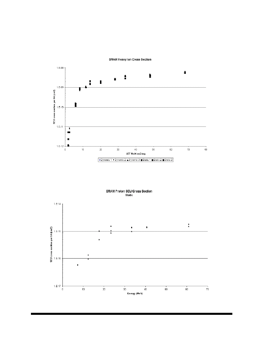
F
IGURE
7. SRAM H
EAVY
I
ON
C
ROSS
S
ECTION
F
IGURE
8. SRAM P
ROTON
SEU C
ROSS
S
ECTION
S
TATIC
M
e
m
o
r
y
11
All data sheets are subject to change without notice
©2005 Maxwell Technologies.
All rights reserved.
16 Megabit (512K x 32-Bit) MCM SRAM
89C1632
01.10.05 Rev 3
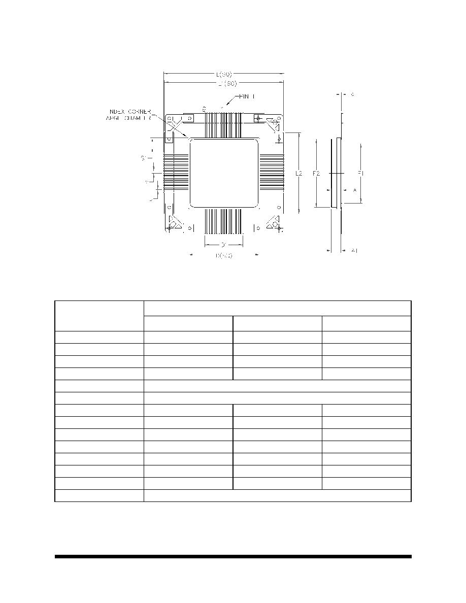
Q68-04
Note: All dimensions in inches
68 P
IN
R
AD
-P
AK
Æ Q
UAD
F
LAT
P
ACKAGE
S
YMBOL
D
IMENSION
M
IN
N
OM
M
AX
A
0.206
0.225
0.244
b
0.015
0.017
0.018
c
0.008
0.009
0.12
D
1.479
1.494
1.509
D1
0.800
e
0.050 BSC
S1
--
0.339
--
F1
1.239
1.244
1.249
F2
1.429
1.434
1.439
L
2.485
2.510
2.545
L1
2.485
2.500
2.505
L2
1.690
1.700
1.710
A1
0.180
0.195
0.210
N
68

M
e
m
o
r
y
12
All data sheets are subject to change without notice
©2005 Maxwell Technologies.
All rights reserved.
16 Megabit (512K x 32-Bit) MCM SRAM
89C1632
01.10.05 Rev 3
Important Notice:
These data sheets are created using the chip manufacturers published specifications. Maxwell Technologies verifies
functionality by testing key parameters either by 100% testing, sample testing or characterization.
The specifications presented within these data sheets represent the latest and most accurate information available to
date. However, these specifications are subject to change without notice and Maxwell Technologies assumes no
responsibility for the use of this information.
Maxwell Technologies' products are not authorized for use as critical components in life support devices or systems
without express written approval from Maxwell Technologies.
Any claim against Maxwell Technologies must be made within 90 days from the date of shipment from Maxwell Tech-
nologies. Maxwell Technologies' liability shall be limited to replacement of defective parts.

M
e
m
o
r
y
13
All data sheets are subject to change without notice
©2005 Maxwell Technologies.
All rights reserved.
16 Megabit (512K x 32-Bit) MCM SRAM
89C1632
01.10.05 Rev 3
Product Ordering Options
1) Products are manufactured and screened to Maxwell Technologies self-defined Class H and Class K.
Model Number
Feature
Option Details
89C1632 RP
Q
X
-XX
Access Time
Screening Flow
Package
Radiation Feature
Base Product
Nomenclature
20 = 20 ns
25 = 25 ns
30 = 30 ns
Multi Chip Module (MCM)
1
K = Maxwell Self-Defined Class K
H = Maxwell Self-Defined Class H
I = Industrial (testing
@ -55∞C, +25∞C, +125∞C)
E = Engineering (testing @ +25∞C)
Q = Quad Flat Pack
RP = R
AD
-P
AK
Æ package
16 Megabit (512K x 32-Bit) MCM
SRAM