 | –≠–ª–µ–∫—Ç—Ä–æ–Ω–Ω—ã–π –∫–æ–º–ø–æ–Ω–µ–Ω—Ç: 9042RPFK | –°–∫–∞—á–∞—Ç—å:  PDF PDF  ZIP ZIP |

1
M
e
m
o
r
y
All data sheets are subject to change without notice
(858) 503-3300 - Fax: (858) 503-3301 - www.maxwell.com
12-Bit, 41 MSPS A/D Converter
9042
©2007 Maxwell Technologies
All rights reserved.
01.07.05 REV 7
F
EATURES
:
∑ Total dose hardness:
- > 300 krad (Si)
SEL > 120 MeV-cm2/mg
∑ 41 MSPS minimum sampling rate
∑ 80 dB Spurious-Free Dynamic Range (SFDR)
∑ Package:
- 28 pin R
AD
-P
AKÆ
flat pack
∑ 595 mW power dissipation
∑ Single 5 volt power supply
∑ On-chip T/H and reference
∑ Two's complement output format
∑ CMOS compatible output levels
D
ESCRIPTION
:
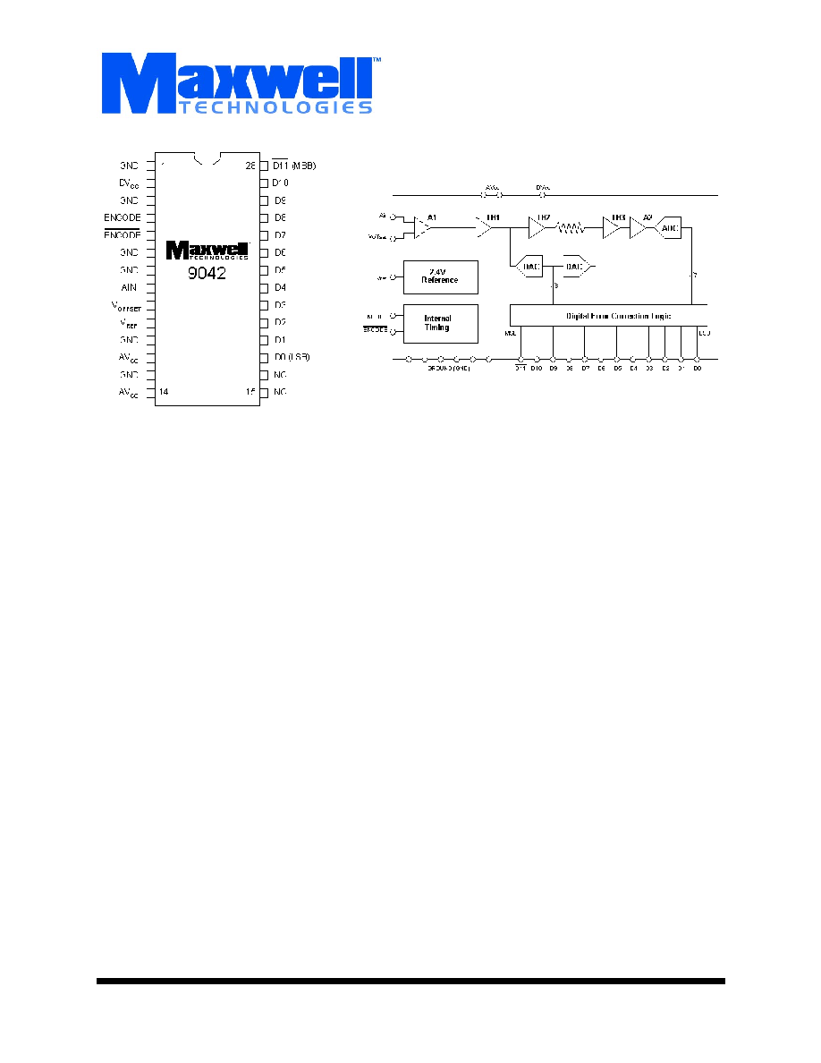
Maxwell Technologies' 9042 12-Bit analog-to-digital converter
features a greater than 300 krad (Si) total dose tolerance.
Using Maxwell's radiation-hardened R
AD
-P
AKÆ
packaging
technology, the 9042 realizes a higher performance, and low
power consumption. All necessary functions, including track-
and-hold (T/H) and reference are included on chip to provide a
complete conversion solution. The 9042 runs off of a single
+5V supply and provides CMOS-compatible digital outputs at
41 MSPS. Designed specifically to address the needs of wide-
band, multichannel receivers, the 9042 maintains 80 dB spuri-
ous-free dynamic range (SFDR) over a bandwidth of 20 MHz.
Noise performance is also exceptional; typical signal to noise
ratio is 68 dB.
Maxwell Technologies' patented R
AD
-P
AKÆ
packaging technol-
ogy incorporates radiation shielding in the microcircuit pack-
age. It eliminates the need for box shielding while providing
the required radiation shielding for a lifetime in an orbit or
space mission. This product is available with screening up to
Maxwell Technologies self-defined Class K.

M
e
m
o
r
y
2
All data sheets are subject to change without notice
©2005 Maxwell Technologies
All rights reserved.
12-Bit, 41 MSPS A/D Converter
9042
01.07.05 REV 7
T
ABLE
1. 9042 P
IN
D
ESCRIPTION
P
IN
S
YMBOL
D
ESCRIPTION
1
GND
Ground
2
DV
CC
5V Power Supply (Digital)
3
GND
Ground
4
ENCODE
Encode Input. Data conversion initiated on rising edge.
5
ENCODE
Complement of ENCODE. Drive differently with ENCODE or bypass
to Ground for single-ended clock mode.
6
GND
Ground
7
GND
Ground
8
AIN
Analog Input.
9
V
OFFSET
Voltage Offset Input. Sets mid-point of analog input range. Normally
tied to V
REF
through 50 Ohm resistor.
10
V
REF
Internal Voltage Reference. Nominally 2.4V; normally tied to V
OFFSET
through 50 Ohm resistor. Bypass to Ground with 0.01 µ F capacitor.
11
GND
Ground
12
AV
CC
5V Power Supply (Analog)
13
GND
Ground
14
AV
CC
5V Power Supply (Analog)
15
NC
No Connects.
16
NC
No Connects.
17
D0 (LSB)
Digital Output Bit (Least Significant Bit).
18 - 27
D1 - D10
Digital Output Bits.
28
D11 (MSB)
1
1.
Output coded as twos compliment
Digital Output Bit (Most Significant Bit).

M
e
m
o
r
y
3
All data sheets are subject to change without notice
©2005 Maxwell Technologies
All rights reserved.
12-Bit, 41 MSPS A/D Converter
9042
01.07.05 REV 7
T
ABLE
2. 9042 A
BSOLUTE
M
AXIMUM
R
ATINGS1
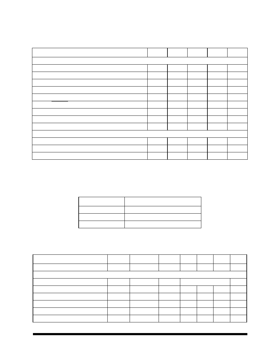
1. A
bsolute maximum ratings are limiting values to be applied individually, and beyond which the serviceability of the circuit may be impaired. Functional operability is not necessarily
implied. Exposure to absolute maximum rating conditions for an extended period of time may affect device reliability.
P
ARAMETER
S
YMBOL
M
IN
T
YPICAL
M
AX
U
NIT
ELECTRICAL
Analog Supply Voltage
AV
CC
0
7
V
Digital Supply Voltage
DV
CC
0
7
V
Analog Input Voltage
A
IN
0.5
4.5
V
Analog Input Current
20
mA
Digital Input Voltage (ENCODE)
0
AV
CC
V
ENCODE, ENCODE Differential Voltage
4
V
Digital Output Current
-40
40
mA
Package Weight
5.25
Grams
Thermal Impedance
JC
2.39
∞C/W
ENVIRONMENTAL
Maximum Junction Temperature
T
J
150
∞C
Operating Temperature Range
T
A
-55
125
∞C
Storage Temperature Range
T
S
-65
150
∞C
T
ABLE
3. D
ELTA
L
IMITS
P
ARAMETER
V
ARIATION
I(AV
CC
)
±10% of specified value in Table 4
I(DV
CC
)
±10% of specified value in Table 4
I
CCTOTAL
±10% of specified value in Table 4
T
ABLE
4. 9042 DC E
LECTRICAL
C
HARACTERISTICS
(AV
CC
= DV
CC
= +5V ±5%; V
REF
TIED
TO
V
OFFSET
THROUGH
50
; T
A
= -55∞C
TO
+125∞C
P
ARAMETER
S
YMBOL
C
ONDITION
S
UBGROUPS
M
IN
T
YP
M
AX
U
NIT
Resolution
12
DC ACCURACY
No Missing Codes
1
-55 to 125∞C
1, 2, 3
Guaranteed
Offset Error
-55 to 125∞C
1, 2, 3
-10
±3
10
mV
Offset Tempco
-55 to 125∞C
1, 2, 3
25
ppm/∞C
Gain Error
-55 to 125∞C
1, 2, 3
-6.5
0
6.5
% FS
Gain Tempco
-55 to 125∞C
1, 2, 3
-50
ppm/∞C
REFERENCE OUT
V
REF
2
25∞C
1
2.3
2.4
2.5
V

M
e
m
o
r
y
4
All data sheets are subject to change without notice
©2005 Maxwell Technologies
All rights reserved.
12-Bit, 41 MSPS A/D Converter
9042
01.07.05 REV 7
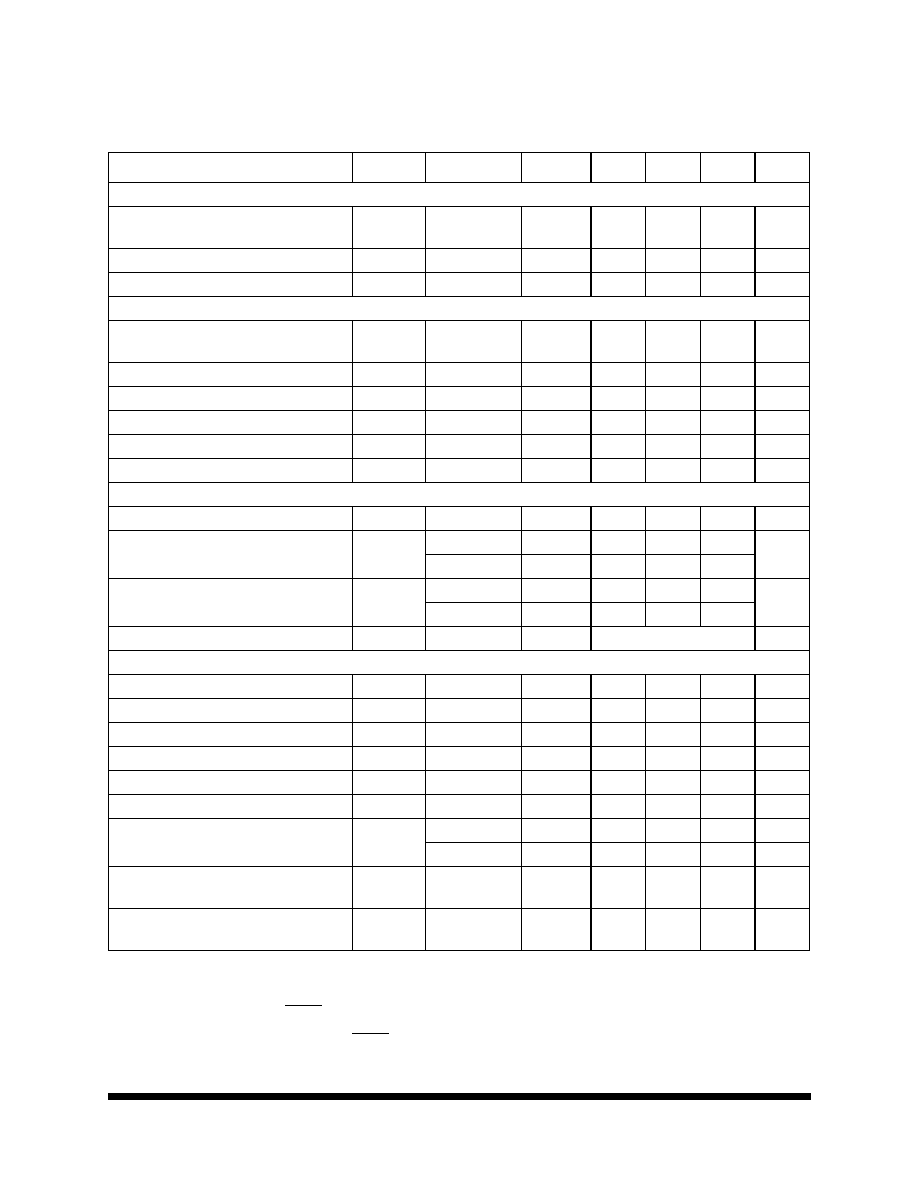
Analog Input (AIN)
Input Voltage Range
1, 2, 3
V
REF
±0.5
V
Input Resistance
-55 to 125∞C
2, 3
200
250
300
Input Capacitance
25∞C
1
7
ENCODE INPUTS
1,3
Logic Compatibility
4
TTL/
CMOS
Logic "1" Voltage
V
IH
-55 to 125∞C
1, 2, 3
2.0
5.0
V
Logic "0" Voltage
V
IL
-55 to 125∞C
1, 2, 3
0
0.8
V
Logic "1" Current (V
INH
= 5V)
I
IH
-55 to 125∞C
1, 2, 3
450
625
800
µ A
Logic "0" Current (V
INL
= 0V)
I
IL
-55 to 125∞C
1, 2, 3
-400
-300
-200
µ A
Input Capacitance
25∞C
1
2.5
pF
DIGITAL OUTPUTS
Logic Compatibility
CMOS
Logic "1" Voltage (I
OH
= 10 µ A)
V
OH
25∞C
1
3.5
4.2
V
-55 to 125∞C
1, 2, 3
3.5
Logic "0" Voltage (I
OL
= 10 µ A)
V
OL
25∞C,125∞C
1, 2
--
0.80
V
-55
3
0.90
Output Coding
Twos Compliment
POWER SUPPLY
Analog Supply Voltage
AV
CC
-55 to 125∞C
1, 2, 3
5.0
V
Analog Supply Current
I
AVCC
-55 to 125∞C
1, 2, 3
--
160
mA
Digital Supply Voltage
DV
CC
-55 to 125∞C
1, 2, 3
5.0
V
Digital Supply Current
I
DVCC
-55 to 125∞C
1, 2, 3
--
20
mA
Supply Current (Total)
I
CCTOTAL
-55 to 125∞C
1, 2, 3
119
180
mA
Power Dissipation
-55 to 125∞C
1, 2, 3
595
990
mW
Power Supply Rejection
PSRR
25∞C
1
-20
±1
20
mV/V
-55 to 125∞C
1, 2, 3
±5
mV/V
Differential Non-linearity
(ENCODE = 20 MSPS)
DNL
-55 to 125∞C
1, 2,3
-1.0
±0.3
1.0
LSB
Integral Non-linearity
(ENCODE = 20 MSPS)
INL
-55 to 125∞C
1, 2, 3
-1.5
±0.75
1.5
LSB
1.
Guaranteed by design.
2.
V
REF
is normally tied to V
OFFSET
through 50 ohms. If V
REF
is used to provide dc offset to other circuits, it should first be buffered
3.
ENCODE driven by single-ended source; ENCODE bypassed to ground through 0.01 µ F capacitor.
4.
ENCODE may also be driven differently in conjunction with ENCODE.
T
ABLE
4. 9042 DC E
LECTRICAL
C
HARACTERISTICS
(AV
CC
= DV
CC
= +5V ±5%; V
REF
TIED
TO
V
OFFSET
THROUGH
50
; T
A
= -55∞C
TO
+125∞C
P
ARAMETER
S
YMBOL
C
ONDITION
S
UBGROUPS
M
IN
T
YP
M
AX
U
NIT

M
e
m
o
r
y
5
All data sheets are subject to change without notice
©2005 Maxwell Technologies
All rights reserved.
12-Bit, 41 MSPS A/D Converter
9042
01.07.05 REV 7
T
ABLE
5. 9042 AC E
LECTRICAL
C
HARACTERISTICS1
(AV
CC
= DV
CC
= +5V ±5%; ENCODE & ENCODE = 41 MSPS; V
REF
TIED
TO
V
OFFSET
THROUGH
50
; T
A
= -55∞C
TO
+125∞C)
P
ARAMETER
S
YMBOL
C
ONDITION
S
UBGROUPS
M
IN
T
YP
M
AX
U
NIT
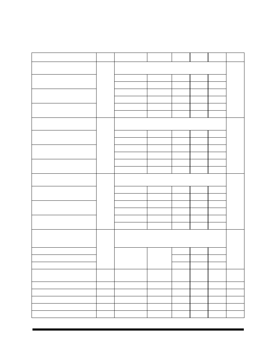
Signal to Noise Ratio
2
Analog Input @ -1 dBFS
SNR
dB
1.2 MHz
25∞C
4
--
68
--
-55 to 125∞C
5, 6
--
67.5
--
9.6 MHz
25∞C
4
--
67.5
--
-55 to 125∞C
5, 6
--
67
--
19.5 MHz
25∞C
4
64
67
--
-55 to 125∞C
5, 6
--
66.5
--
SINAD
3
Analog Input @ -1 dBFS
SINAD
dB
1.2 MHz
25∞C
4
--
67.5
--
-55 to 125∞C
5, 6
--
67
--
9.6 MHz
25∞C
4
--
67.5
--
-55 to 125∞C
5, 6
--
67
--
19.5 MHz
25∞C
4
64
67
--
-55 to 125∞C
5, 6
--
66.5
--
Worst Spur
4
Analog Input @ -1 dBFS
dBc
1.2 MHz
25∞C
4
--
80
--
-55 to 125∞C
5, 6
--
78
--
9.6 MHz
25∞C
4
--
80
--
-55 to 125∞C
5, 6
--
78
--
19.5 MHz
25∞C
4
73
80
--
-55 to 125∞C
5, 6
--
78
--
Small Signal Spurios Free Dynamic
Range (w/ Dither)
5
Analog Input @
SFDR
dBFS
1.2 MHz
-55 to 125∞C
4, 5, 6
--
90
--
9.6 MHz
--
90
--
19.5 MHz
--
90
--
Two-Tone IMD Rejection
6
F1, F2 @ -7 dBFS
-55 to 125∞C
4, 5, 6
--
80
--
dBc
Two-Tone SFDR (w/Dither)
7
-55 to 125∞C
4, 5, 6
--
90
--
dBFS
Thermal Noise
25∞C
9
--
0.33
--
LSB rms
Analog Input bandwidth
8
25∞C
9
100
MHz
Transient Response
8
25∞C
9
10
ns
Overvoltage Recovery Time
8
25∞C
9
25
ns
